Method For Etching Features In A Stack
BELAU; Leonid ; et al.
U.S. patent application number 15/798831 was filed with the patent office on 2019-05-02 for method for etching features in a stack. The applicant listed for this patent is Lam Research Corporation. Invention is credited to Leonid BELAU, Eric HUDSON, Francis Sloan ROBERTS.
| Application Number | 20190131135 15/798831 |
| Document ID | / |
| Family ID | 66245617 |
| Filed Date | 2019-05-02 |


| United States Patent Application | 20190131135 |
| Kind Code | A1 |
| BELAU; Leonid ; et al. | May 2, 2019 |
METHOD FOR ETCHING FEATURES IN A STACK
Abstract
A method for etching features in a stack below a carbon containing mask is provided. The stack is cooled to a temperature below -20.degree. C. An etch gas is provided comprising a free fluorine providing component, a hydrogen containing component, a hydrocarbon containing component, and a fluorocarbon containing component. A plasma is generated from the etch gas. A bias is provided with a magnitude of at least about 400 volts to accelerate ions from the plasma to the stack. Features are selectively etched in the stack with respect to the carbon containing mask.
| Inventors: | BELAU; Leonid; (Pleasanton, CA) ; HUDSON; Eric; (Berkeley, CA) ; ROBERTS; Francis Sloan; (Redwood City, CA) | ||||||||||
| Applicant: |
|
||||||||||
|---|---|---|---|---|---|---|---|---|---|---|---|
| Family ID: | 66245617 | ||||||||||
| Appl. No.: | 15/798831 | ||||||||||
| Filed: | October 31, 2017 |
| Current U.S. Class: | 1/1 |
| Current CPC Class: | H01L 21/31116 20130101; H01L 21/31144 20130101; H01L 21/308 20130101; H01L 21/3065 20130101 |
| International Class: | H01L 21/3065 20060101 H01L021/3065; H01L 21/311 20060101 H01L021/311; H01L 21/308 20060101 H01L021/308 |
Claims
1. A method for etching features in a stack below a carbon containing mask, comprising: cooling the stack to a temperature below -20.degree. C.; providing an etch gas comprising a free fluorine providing component, a hydrogen containing component, a hydrocarbon containing component, and a fluorocarbon containing component; generating a plasma from the etch gas; providing a bias with a magnitude of at least about 400 volts to accelerate ions from the plasma to the stack; and selectively etching features in the stack with respect to the carbon containing mask.
2. The method, as recited in claim 1, wherein the carbon containing mask is amorphous carbon.
3. The method, as recited in claim 1, wherein the etch gas further comprises an iodine containing component.
4. The method, as recited in claim 1, wherein the etch gas is oxygen free and free from both C.sub.4F.sub.8 and C.sub.4F.sub.6.
5. The method, as recited in claim 1, wherein the etch gas comprises NF.sub.3, H.sub.2, CF.sub.3I, CH.sub.3F, and CH.sub.2F.sub.2.
6. The method, as recited in claim 5, wherein the etch gas further comprises at least one of C.sub.4F.sub.8, C.sub.3F.sub.8, C.sub.4F.sub.6, SF.sub.6, O.sub.2, CF.sub.4, CH.sub.4, or CHF.sub.3.
7. The method, as recited in claim 1, wherein the stack is supported on a chuck in an etch chamber, the method further comprising cooling the chuck to a temperature below -40.degree. C.
8. The method, as recited in claim 1, wherein the carbon containing mask is amorphous carbon and the stack includes a plurality of silicon oxide and silicon nitride bilayers.
9. The method, as recited in claim 8, wherein the plurality of silicon oxide and silicon nitride bilayers include at least 48 bilayers.
10. The method, as recited in claim 8, wherein the stack does not have a silicon containing mask.
11. The method, as recited in claim 1, wherein the free fluorine providing component comprises NF.sub.3 and the hydrogen containing component comprises H.sub.2.
12. The method, as recited in claim 1, wherein the free fluorine providing component comprises NF.sub.3, the hydrogen containing component comprises H.sub.2, and wherein the etch gas comprises a hydrofluorocarbon-containing component which provides the hydrocarbon containing component and the fluorocarbon containing component.
13. The method, as recited in claim 1, wherein the etch gas further comprises CF.sub.3I.
14. The method, as recited in claim 1, wherein the etch gas further comprises CF.sub.3I, and wherein the etch gas comprises a hydrofluorocarbon-containing component which provides the hydrocarbon containing component and the fluorocarbon containing component.
15. The method, as recited in claim 1, wherein the free fluorine providing component provides free fluorine when excited to generate the plasma.
16. The method, as recited in claim 1, wherein the features have a depth to neck aspect ratio of at least 30:1.
17. The method, as recited in claim 1, wherein the free fluorine providing component includes at least one of NF.sub.3 or SF.sub.6.
Description
INCORPORATION BY REFERENCE
[0001] The present disclosure incorporates by reference for all purposes the patent application entitled "GAS ADDITIVES FOR SIDEWALL PASSIVATION DURING HIGH ASPECT RATIO CRYOGENIC ETCH" by Hudson et al. filed on Mar. 30, 2017, U.S. application Ser. No. 15/475,021.
BACKGROUND
Field
[0002] The disclosure relates to a method of forming semiconductor devices on a semiconductor wafer. More specifically, the disclosure relates to etching a stack in the formation of memory.
[0003] In forming semiconductor devices, etch layers may be etched to form memory holes or lines. Some semiconductor devices may be formed by etching a stack of bilayers of silicon oxide and silicon nitride (ONON). Such stacks may be used in memory applications, such as in forming dynamic random access memory (DRAM) and three dimensional "negative and" gates (3D NAND).
SUMMARY
[0004] To achieve the foregoing and in accordance with the purpose of the present disclosure, a method for etching features in a stack below a carbon containing mask is provided. The stack is cooled to a temperature below -20.degree. C. An etch gas is provided comprising a free fluorine providing component, a hydrogen containing component, a hydrocarbon containing component, and a fluorocarbon containing component. A plasma is generated from the etch gas. A bias is provided with a magnitude of at least about 400 volts to accelerate ions from the plasma to the stack. Features are selectively etched in the stack with respect to the carbon containing mask.
[0005] These and other features of the present disclosure will be described in more details below in the detailed description and in conjunction with the following figures.
BRIEF DESCRIPTION OF THE DRAWINGS
[0006] The present disclosure is illustrated by way of example, and not by way of limitation, in the figures of the accompanying drawings and in which like reference numerals refer to similar elements and in which:
[0007] FIG. 1 is a high level flow chart of an embodiment.
[0008] FIGS. 2A-B are schematic cross-sectional views of a stack processed according to an embodiment.
[0009] FIG. 3 is a schematic view of a etch chamber that may be used in an embodiment.
[0010] FIG. 4 is a schematic view of a computer system that may be used in practicing an embodiment.
DETAILED DESCRIPTION OF THE PREFERRED EMBODIMENTS
[0011] The present disclosure will now be described in detail with reference to a few preferred embodiments thereof as illustrated in the accompanying drawings. In the following description, numerous specific details are set forth in order to provide a thorough understanding of the present disclosure. It will be apparent, however, to one skilled in the art, that the present disclosure may be practiced without some or all of these specific details. In other instances, well known process steps and/or structures have not been described in detail in order to not unnecessarily obscure the present disclosure.
[0012] FIG. 1 is a high level flow chart of an embodiment. In this embodiment, a stack is placed in an etch chamber (step 104). The stack is disposed below a carbon containing patterned mask. The stack is cooled to a temperature below -20.degree. C. (step 108). An etch gas is provided by flowing the etch gas into the etch chamber, wherein the etch gas comprises a free fluorine providing component, a hydrogen containing component, a hydrocarbon containing component, and a fluorocarbon containing component (step 112). The etch gas is formed into an etch plasma (step 116). The stack is exposed to the plasma (step 120). A bias is provided with a magnitude of at least 400 volts to accelerate ions from the plasma to the stack (step 124). The stack is selectively etched with respect to the carbon containing patterned mask by the etch plasma (step 128). The stack is removed from the etch chamber (step 132).
EXAMPLE
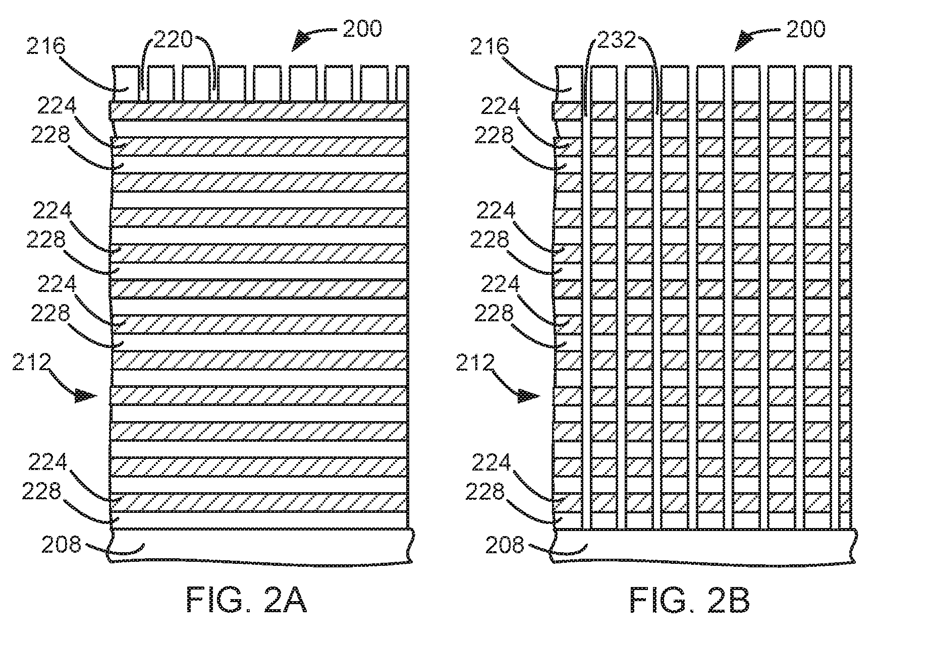
[0013] In an exemplary embodiment, a stack is placed in an etch chamber (step 104). FIG. 2A is a schematic cross-sectional view of a stack 200, which in this embodiment comprises a substrate 208 under a plurality of bilayers 212, which is disposed below a carbon containing patterned mask 216. In this example, one or more layers may be disposed between the substrate 208 and the plurality of bilayers 212 or the plurality of bilayers 212 and the carbon containing patterned mask 216. However, this embodiment does not have a silicon containing mask above the plurality of bilayers 212 or above the carbon containing patterned mask 216. In this example, the carbon containing patterned mask 216 is amorphous carbon. In this example, patterned mask pattern provides mask features 220 for high aspect ratio contacts. In some embodiments, the mask features are formed before the substrate is placed in the etch chamber. In other embodiments, the mask features 220 are formed while the substrate is in the etch chamber. In this embodiment, the plurality of bilayers 212 are bilayers of a layer of silicon oxide 224 and a layer of silicon nitride 228.
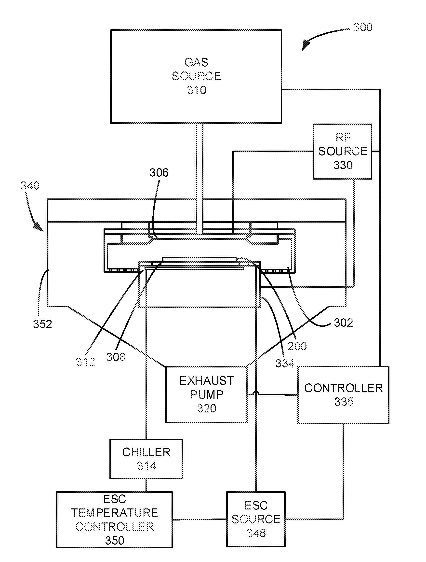
[0014] FIG. 3 is a schematic view of an etch reactor that may be used in an embodiment. In one or more embodiments, an etch reactor 300 comprises a gas distribution plate 306 providing a gas inlet and an electrostatic chuck (ESC) 308, within an etch chamber 349, enclosed by a chamber wall 352. Within the etch chamber 349, a stack 200 is positioned on over the ESC 308. The ESC 308 may provide a bias from the ESC source 348. An etch gas source 310 is connected to the etch chamber 349 through the distribution plate 306. An ESC temperature controller 350 is connected to a chiller 314. In this embodiment, the chiller 314 provides a coolant to channels 312 in or near the ESC 308. A radio frequency (RF) source 330 provides RF power to a lower electrode and/or an upper electrode, which in this embodiment are the ESC 308 and the gas distribution plate 306. In an exemplary embodiment, 400 kHz, 60 MHz, and optionally 2 MHz, 27 MHz power sources make up the RF source 330 and the ESC source 348. In this embodiment, the upper electrode is grounded. In this embodiment, one generator is provided for each frequency. In other embodiments, the generators may be in separate RF sources, or separate RF generators may be connected to different electrodes. For example, the upper electrode may have inner and outer electrodes connected to different RF sources. Other arrangements of RF sources and electrodes may be used in other embodiments. A controller 335 is controllably connected to the RF source 330, the ESC source 348, an exhaust pump 320, and the etch gas source 310. An example of such a etch chamber is the Exelan Flex.TM. etch system manufactured by Lam Research Corporation of Fremont, Calif. The process chamber can be a CCP (capacitive coupled plasma) reactor or an ICP (inductive coupled plasma) reactor.
[0015] FIG. 4 is a high level block diagram showing a computer system 400, which is suitable for implementing a controller 335 used in embodiments. The computer system may have many physical forms ranging from an integrated circuit, a printed circuit board, and a small handheld device up to a huge super computer. The computer system 400 includes one or more processors 402, and further can include an electronic display device 404 (for displaying graphics, text, and other data), a main memory 406 (e.g., random access memory (RAM)), storage device 408 (e.g., hard disk drive), removable storage device 410 (e.g., optical disk drive), user interface devices 412 (e.g., keyboards, touch screens, keypads, mice or other pointing devices, etc.), and a communication interface 414 (e.g., wireless network interface). The communication interface 414 allows software and data to be transferred between the computer system 400 and external devices via a link. The system may also include a communications infrastructure 416 (e.g., a communications bus, cross-over bar, or network) to which the aforementioned devices/modules are connected.
[0016] Information transferred via communications interface 414 may be in the form of signals such as electronic, electromagnetic, optical, or other signals capable of being received by communications interface 414, via a communication link that carries signals and may be implemented using wire or cable, fiber optics, a phone line, a cellular phone link, a radio frequency link, and/or other communication channels. With such a communications interface, it is contemplated that the one or more processors 402 might receive information from a network, or might output information to the network in the course of performing the above-described method steps. Furthermore, method embodiments may execute solely upon the processors or may execute over a network such as the Internet, in conjunction with remote processors that share a portion of the processing.
[0017] The term "non-transient computer readable medium" is used generally to refer to media such as main memory, secondary memory, removable storage, and storage devices, such as hard disks, flash memory, disk drive memory, CD-ROM and other forms of persistent memory and shall not be construed to cover transitory subject matter, such as carrier waves or signals. Examples of computer code include machine code, such as produced by a compiler, and files containing higher level code that are executed by a computer using an interpreter. Computer readable media may also be computer code transmitted by a computer data signal embodied in a carrier wave and representing a sequence of instructions that are executable by a processor.
[0018] After the stack 200 has been placed into the etch chamber 300, the stack is cooled to a temperature below -20.degree. C. (step 108). An etch gas comprising a free fluorine providing component, a hydrogen containing component, a hydrocarbon containing component, and a fluorocarbon containing component is flowed into the etch chamber (step 112). In this example, the etch gas is 2-150 sccm NF.sub.3, 20-300 sccm H.sub.2, 2-40 sccm CF.sub.3I, 10-60 sccm CH.sub.3F, and 0-100 sccm CH.sub.2F.sub.2. In this example, a pressure of 5 to 60 mTorr is provided. The etch gas is formed into an etch plasma (step 116). This may be accomplished by providing an excitation RF with a frequency of 60 MHz at 200 to 8000 watts. The stack 200 is exposed to the plasma (step 120). A bias with a magnitude of at least about 400 volts is provided (step 124). In this embodiment, the high bias is provided by providing an RF with a frequency of 400 kHz at 2 kW to 18 kW. The bias causes ions to be accelerated to the stack 200 causing the selective etching of high aspect ratio etch features into the stack 200 with respect to the carbon containing patterned mask (step 128). The plasma is maintained for 180 to 3600 seconds. The etch is able to etch both the silicon oxide and silicon nitride layers. The substrate is then removed from the etch chamber (step 132).
[0019] FIG. 2B is a cross-sectional view of the stack 200 after the contacts 232 have been etched. The contacts are high aspect ratio contacts. Preferably, the high aspect ratio contacts have a height to CD width ratio of greater than 100:1. More preferably, the contacts have a neck to etch depth aspect ratio of greater than 30:1.
[0020] The etch process is able to selectively etch the silicon oxide and silicon nitride layers with respect to amorphous carbon with a selectivity of greater than 5:1, while etching high aspect ratio features. The resulting features also have reduced bowing, striation, distorting, capping, and tapering. In addition, this embodiment allows the use of a carbon containing patterned mask, such as amorphous carbon, without requiring a silicon containing mask such as polysilicon, which reduces costs and defects.
[0021] Previous processes that use an etch, where the stack is processed at a temperature above -20.degree. C., relied on a fluorocarbon chemistry to etch and provide sidewall protection. Such a process resulted in a mask to silicon oxide and silicon nitride etch selectivity of less than 5:1. Sidewall protection was provided by polymer deposition, which is controlled by the concentration of carbon, where a higher concentration of carbon increases sidewall deposition, and by oxygen, where a higher concentration of oxygen consumes the deposited polymer. The higher concentration of oxygen also increased the consumption of the mask. Some previous processes used a silicon containing mask.
[0022] The above embodiment increases etch rate and improves contact shape/striation compared to a conventional approach. Without being bound by theory, it is proposed that a fluorine-rich fluorocarbon polymer at the high aspect ratio etch front is enabled by the lower wafer temperature. This increases the silicon oxide and silicon nitride etch rate, while building up less carbon at the etch front. A reduced carbon-rich polymer buildup at the etch front also improves contact shape and reduces sidewall striation. In addition, the higher selectivity of silicon oxide and silicon nitride to carbon mask could be achieved. This allows for the use of a thinner carbon containing mask, which improves control and performance of the carbon mask open process.
[0023] In some embodiments, to cool the stack to a temperature below -20.degree. C., the electrostatic chuck is cooled to a temperature below -60.degree. C. In other embodiments, it is believed that when the chuck is cooled to a temperature between -30.degree. C. to -200.degree. C. the process is improved. In other embodiments, the chuck is cooled to a temperature below -40.degree. C. to -200.degree. C. In some embodiments, the stack is cooled to a temperature between -30.degree. C. to -200.degree. C.
[0024] In some embodiments, the etch gas comprises a free fluorine providing component, a hydrogen containing component, a hydrocarbon containing component, and a fluorocarbon containing component and an iodine containing component. A free fluorine providing component is defined as a component that will normally break down in plasma to provide free-fluorine, such as NF.sub.3 and SF.sub.6. Hydrogen containing components are preferably H.sub.2, CH.sub.3F and CH.sub.2F.sub.2. In addition, various components may form a single polyatomic molecule. For example, CF.sub.3I may provide both the fluorocarbon containing component and the iodine containing component. In addition, a hydrofluorocarbon-containing component may provide the hydrocarbon containing component and the fluorocarbon containing component. Iodine containing components may be selected from the group comprising at least one of trifluoroiodomethane (CF.sub.3I), pentafluoroiodoethane (C.sub.2IF.sub.5), tetrafluorodiiodoethane (C.sub.2I.sub.2F.sub.4). Without being bound by theory, it is believed that the iodine from the iodine containing component provides an improved sidewall passivation, which helps to reduce bowing. By using a low substrate temperature in combination with certain reactants, a high quality protective film can be formed on sidewalls of the partially etched features during etching. The low temperature also allows some embodiments where the etch gas is oxygen free and free from both C.sub.4F.sub.8, C.sub.4F.sub.6, and C.sub.3F.sub.8. In other embodiments, the etch gas comprises NF.sub.3, H.sub.2, CF.sub.3I, CH.sub.3F, and CH.sub.2F.sub.2. In some of the embodiments, the etch gas further comprises at least one of C.sub.4F.sub.8, C.sub.4F.sub.6, C.sub.3F.sub.8, SF.sub.6, CF.sub.4, CH.sub.4, or CHF.sub.3.
[0025] The ONON stack may be etched to form contact holes or trenches in making a 3D NAND memory device. Other embodiments may etch contact holes to be used in MOC and MOA, which are first metal contacts used to control 3D NAND junctions. Other embodiments may be used for DRAM Capacitor etching. Embodiments provide for a CD less than 100 nm with an etch depth of greater than 20 microns. In other embodiments, the etch depth is greater than 3 microns. Such embodiments allow the etching of at least 48 bilayers of silicon oxide and silicon nitride in a single etch step using a single amorphous carbon mask with a thickness of less than 1 microns.
[0026] In some embodiments, the stack may be a single layer of silicon oxide or silicon nitride. In other embodiments, the stack may be a single layer or multiple layers of other silicon containing materials.
[0027] The above embodiment used a bias with a magnitude of at least 400 volts. It has been found that a bias with a magnitude of at least 1000 volts would provide an improved etch. It is believed that a bias with a magnitude of at least 2000 volts would provide a further improved etch. Without being bound by theory it is believed that the higher bias would allow for a higher aspect ratio etch, while taking advantage of other features, which allows for the use of an amorphous carbon mask and reducing striation and bowing.
[0028] In some embodiments, liquid nitrogen is used as a coolant that is flowed through the chuck or bottom electrode to provide cooling. In other embodiments, liquid Vertel Sinera.TM. manufactured by DuPont Corporation of Wilmington, Del. may be used as the coolant.
[0029] While this disclosure has been described in terms of several preferred embodiments, there are alterations, modifications, permutations, and various substitute equivalents, which fall within the scope of this disclosure. It should also be noted that there are many alternative ways of implementing the methods and apparatuses of the present disclosure. It is therefore intended that the following appended claims be interpreted as including all such alterations, modifications, permutations, and various substitute equivalents as fall within the true spirit and scope of the present disclosure.
* * * * *
D00000
D00001
D00002
D00003
D00004
XML
uspto.report is an independent third-party trademark research tool that is not affiliated, endorsed, or sponsored by the United States Patent and Trademark Office (USPTO) or any other governmental organization. The information provided by uspto.report is based on publicly available data at the time of writing and is intended for informational purposes only.
While we strive to provide accurate and up-to-date information, we do not guarantee the accuracy, completeness, reliability, or suitability of the information displayed on this site. The use of this site is at your own risk. Any reliance you place on such information is therefore strictly at your own risk.
All official trademark data, including owner information, should be verified by visiting the official USPTO website at www.uspto.gov. This site is not intended to replace professional legal advice and should not be used as a substitute for consulting with a legal professional who is knowledgeable about trademark law.