Methods For Forming A Semiconductor Structure And Related Semiconductor Structures
Kohen; David ; et al.
U.S. patent application number 15/798201 was filed with the patent office on 2019-05-02 for methods for forming a semiconductor structure and related semiconductor structures. The applicant listed for this patent is ASM IP Holding B.V.. Invention is credited to David Kohen, Andrew Kretzschmar, Harald Benjamin Profijt.
| Application Number | 20190131124 15/798201 |
| Document ID | / |
| Family ID | 66244155 |
| Filed Date | 2019-05-02 |


| United States Patent Application | 20190131124 |
| Kind Code | A1 |
| Kohen; David ; et al. | May 2, 2019 |
METHODS FOR FORMING A SEMICONDUCTOR STRUCTURE AND RELATED SEMICONDUCTOR STRUCTURES
Abstract
A method for forming a forming a semiconductor structure is disclosed. The method may include: forming a silicon oxide layer on a surface of a substrate, depositing a silicon germanium (Si.sub.1-xGe.sub.x) seed layer directly on the silicon oxide layer, and depositing a germanium (Ge) layer directly on the silicon germanium (Si.sub.1-xGe.sub.x) seed layer. Semiconductor structures including a germanium (Ge) layer deposited on silicon oxide utilizing an intermediate silicon germanium (Si.sub.1-xGe.sub.x) seed layer are also disclosed.
| Inventors: | Kohen; David; (Phoenix, AZ) ; Profijt; Harald Benjamin; (Veldhoven, NL) ; Kretzschmar; Andrew; (Austin, TX) | ||||||||||
| Applicant: |
|
||||||||||
|---|---|---|---|---|---|---|---|---|---|---|---|
| Family ID: | 66244155 | ||||||||||
| Appl. No.: | 15/798201 | ||||||||||
| Filed: | October 30, 2017 |
| Current U.S. Class: | 1/1 |
| Current CPC Class: | H01L 21/02164 20130101; H01L 21/02532 20130101; H01L 27/11582 20130101; H01L 21/02488 20130101; H01L 29/165 20130101; H01L 21/0245 20130101; H01L 21/02595 20130101; H01L 27/11556 20130101; H01L 29/1054 20130101; H01L 21/0262 20130101; H01L 21/02502 20130101 |
| International Class: | H01L 21/02 20060101 H01L021/02; H01L 29/165 20060101 H01L029/165 |
Claims
1. A method for forming a semiconductor structure, the method comprising: forming a silicon oxide layer on a surface of a substrate; depositing a silicon germanium (Si.sub.1-xGe.sub.x), where x is between 0.01 and 0.3 seed layer directly on the silicon oxide layer; and depositing a germanium (Ge) layer directly on the silicon germanium (Si.sub.1-xGe.sub.x) seed layer, wherein the silicon germanium (Si.sub.1-xGe.sub.x) seed layer has a thickness of less than 30 nm.
2. (canceled)
3. The method of claim 1, wherein depositing the silicon germanium (Si.sub.1-xGe.sub.x) seed layer further comprises, depositing the silicon germanium (Si.sub.1-xGe.sub.x) seed layer at a substrate temperature of between approximately 250.degree. C. and approximately 500.degree. C.
4. The method of claim 1, wherein depositing the silicon germanium (Si.sub.1-xGe.sub.x) seed layer further comprises, depositing the silicon germanium (Si.sub.1-xGe.sub.x) seed at a reaction chamber pressure of between approximately 10 Torr and approximately 760 Torr.
5. The method of claim 1, wherein depositing the silicon germanium (Si.sub.1-xGe.sub.x) seed layer further comprises flowing germane (GeH.sub.4) as a germanium precursor.
6. The method of claim 1, wherein depositing the silicon germanium (Si.sub.1-xGe.sub.x) seed layer further comprises flowing trisilane (Si.sub.3H.sub.8) as a silicon precursor.
7. The method of claim 1, wherein the silicon germanium (Si.sub.1-xGe.sub.x) seed layer has a thickness of between 1 nanometer to 10 nanometers.
8. The method of claim 1, wherein the silicon germanium (Si.sub.1-xGe.sub.x) seed layer has an amorphous crystalline structure.
9. The method of claim 1, wherein the silicon germanium (Si.sub.1-xGe.sub.x) seed layer has a polycrystalline crystalline structure.
10. The method of claim 1, wherein the germanium layer has a thickness of between 5 nanometers to 15 nanometers.
11. The method of claim 1, wherein depositing the germanium layer occurs at a substrate temperature of between approximately 300.degree. C. and approximately 350.degree. C.
12. The method of claim 1, wherein depositing the germanium layer further comprises flowing germane (GeH.sub.4) as a germanium precursor.
13. The method of claim 1, wherein the germanium layer has a polycrystalline crystalline structure.
14. The method of claim 1, wherein the germanium layer has a substantially monocrystalline crystalline structure.
15. The method of claim 1, wherein the germanium layer has a carrier mobility of greater than 30 cm.sup.2/(Vs).
16. The method of claim 1, further comprising heating the germanium layer to a temperature greater than 400.degree. C. to recrystallize the germanium layer.
17. The method of claim 1, wherein the germanium layer comprises a channel region of a semiconductor device structure.
18. The method of claim 1, further comprising depositing an additional silicon dioxide layer directly on the germanium layer.
19. A semiconductor structure comprising: a silicon dioxide (SiO.sub.2) layer disposed directly on the surface of a substrate; a silicon germanium (Si.sub.1-xGe.sub.x) seed layer disposed directly on the silicon dioxide layer; and a germanium (Ge) layer disposed directly on the silicon germanium (Si.sub.1-xGe.sub.x) seed layer.
20. The semiconductor structure of claim 19, wherein the silicon germanium (Si.sub.1-xGe.sub.x) seed layer has a germanium composition of between x=0.01 and x=0.30.
21. The semiconductor structure of claim 19, wherein the silicon germanium (Si.sub.1-xGe.sub.x) seed layer has a thickness of between 3 nanometers and 10 nanometers.
22. The semiconductor structure of claim 19, wherein the germanium layer has a thickness of between 5 nanometers and 15 nanometers.
23. The semiconductor structure of claim 19, wherein the germanium layer has a carrier mobility of greater than 30 cm.sup.2(Vs).
24. The semiconductor structure of claim 19, wherein the germanium layer comprises a channel region of a semiconductor device structure.
25. The semiconductor structure of claim 19, wherein the channel region of the semiconductor device structure comprises the channel region of a memory element.
26. The semiconductor structure of claim 19, further comprising an additional silicon dioxide (SiO.sub.2) layer disposed directly over the germanium (Ge) layer.
Description
FIELD OF INVENTION
[0001] The present disclosure generally relates to methods for forming a semiconductor structure and particular to methods for depositing a germanium layer over a silicon oxide layer utilizing an intermediate silicon germanium (Si.sub.1-xGe.sub.x) seed layer. The present disclosure also generally relates to semiconductor structures and particularly semiconductor structures including a germanium layer deposited over a silicon oxide layer utilizing an intermediate silicon germanium (Si.sub.1-xGe.sub.x) seed layer.
BACKGROUND OF THE DISCLOSURE
[0002] As semiconductor devices continue to decrease in size in advanced technology nodes, a number of challenges arise in developing higher performance devices. One approach to increase the performance of semiconductor devices is to increase the carrier mobility, i.e., electrons and/or holes, in the channel region of the device. Although it is possible to obtain higher carrier mobilities with strained silicon, much higher mobilities may be achieved by using a different semiconductor material in the channel region other than silicon. For example, hole mobility in germanium (Ge) is known to be much higher than in silicon. However, using a bulk material other than silicon presents a huge integration and device design challenge. For example, diffusion enhancement of n-type dopants in germanium (Ge) makes it very challenging to obtain advantageous ultra-shallow junctions. Moreover, the majority of process steps commonly utilized in silicon device fabrication, such as silicidation and surface cleaning, are currently unsatisfactory for high mobility materials. As a result, it continues to be easier and more cost effective to use silicon as a bulk material and use the high mobility materials only in the channel regions.
[0003] In order to achieve a germanium (Ge) channel in a semiconductor device structure, such as, for example, a field effect transistor, or memory element, deposition methods may be utilized to deposit the germanium (Ge) high mobility channel over a suitable substrate. In some semiconductor device applications it may be necessary to deposit a germanium layer over the surface of a silicon oxide (e.g., SiO.sub.2). However, germanium (Ge) deposition directly on a silicon oxide surface may be problematic because the common germanium deposition processes, utilizing germane (GeH.sub.4) as the germanium precursor, do not deposit germanium directly on silicon oxide surfaces. It has been theorized, that the tendency of germanium to refrain from depositing on a silicon oxide surface may be due to a low density of germanium absorption sites available on a silicon oxide surface, such as, silicon dioxide (SiO.sub.2).
[0004] Accordingly, methods for forming a germanium layer over a silicon oxide surface are desirable for fabricating semiconductor structures including a high mobility germanium (Ge) channel region.
SUMMARY OF THE DISCLOSURE
[0005] In accordance with at least one embodiment of the disclosure, a method for forming a semiconductor structure is disclosed. The method may comprise: forming a silicon oxide layer on a surface of a substrate; depositing a silicon germanium (Si.sub.1-xGe.sub.x) seed layer directly on the silicon oxide layer; and depositing a germanium layer directly on the silicon germanium (Si.sub.1-xGe.sub.x) seed layer.
[0006] The embodiments of the disclosure may also provide semiconductor structures comprising: a silicon oxide layer disposed directly on the surface of a substrate; a silicon germanium (Si.sub.1-xGe.sub.x) seed layer disposed directly on the silicon oxide layer; and a germanium (Ge) layer disposed directly on the silicon germanium (Si.sub.1-xG.sub.x) seed layer.
[0007] For the purpose of summarizing the invention and the advantages achieved over the prior art, certain objects and advantages of the invention have been described herein above. Of course, it is to be understood that not necessarily all such objects or advantages may be achieved in accordance with any particular embodiment of the invention. Thus, for example, those skilled in the art will recognize that the invention may be embodied or carried out in a manner that achieves or optimizes one advantage or group of advantages as taught or suggested herein without necessarily achieving other objects or advantages as may be taught or suggested herein.
[0008] All of these embodiments are intended to be within the scope of the invention herein disclosed. These and other embodiments will become readily apparent to those skilled in the art from the following detailed description of certain embodiments having reference to the attached figures, the invention not being limited to any particular embodiment(s) disclosed.
BRIEF DESCRIPTION OF THE DRAWING FIGURES
[0009] While the specification concludes with claims particularly pointing out and distinctly claiming what are regarded as embodiments of the invention, the advantages of embodiments of the disclosure may be more readily ascertained from the description of certain examples of the embodiments of the disclosure when read in conjunction with the accompanying drawing, in which:
[0010] FIG. 1 illustrates a process flow diagram illustrating an exemplary method in accordance with the embodiments of the disclosure;
[0011] FIGS. 2A, 2B, 2C, 2D and 2E illustrate cross sectional schematic diagrams of an exemplary process flow in accordance with the embodiments of the disclosure;
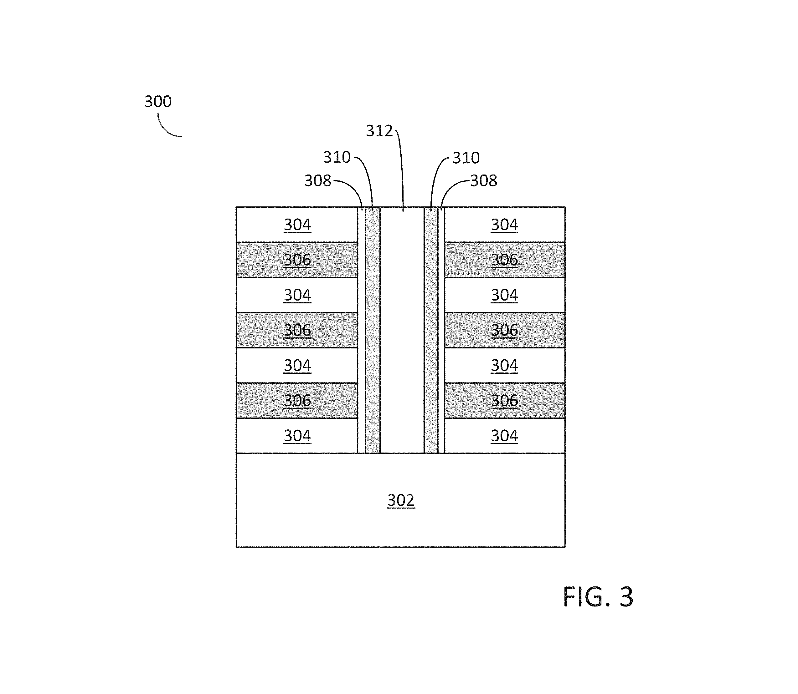
[0012] FIG. 3 illustrates a semiconductor device structure including a germanium (Ge) layer formed by the embodiments of the disclosure.
[0013] It will be appreciated that elements in the figures are illustrated for simplicity and clarity and have not necessarily been drawn to scale. For example, the dimensions of some of the elements in the figures may be exaggerated relative to other elements to help improve understanding of illustrated embodiments of the present disclosure.
DETAILED DESCRIPTION OF EXEMPLARY EMBODIMENTS
[0014] Although certain embodiments and examples are disclosed below, it will be understood by those in the art that the invention extends beyond the specifically disclosed embodiments and/or uses of the invention and obvious modifications and equivalents thereof. Thus, it is intended that the scope of the invention disclosed should not be limited by the particular disclosed embodiments described below.
[0015] As used herein, the term "substrate" may refer to any underlying material or materials that may be used, or upon which, a device, a circuit or a film may be formed.
[0016] As used herein, the term "silicon germanium" and "Si.sub.1-xGe.sub.x" may refer to an alloy of silicon and germanium, wherein the ratio of germanium to silicon may range as 1.gtoreq.x.gtoreq.0.
[0017] As used herein, the term "chemical vapor deposition" may refer to any process wherein a substrate is exposed to one or more volatile precursors, which react and/or decompose on a substrate surface to produce a desired deposition.
[0018] In the specification, it will be understood that the term "on" or "over" may be used to describe a relative location relationship, another element or layer may be directly on the mentioned layer, or another layer (an intermediate layer) or element may be intervened therebetween, or a layer may be disposed on a mentioned layer but not completely cover a surface of the mentioned layer. Therefore, unless the term "directly" is separately used, the term "on" or "over" will be construed to be a relative concept. Similarly to this, it will be understood the term "under," "underlying," or "below" will be construed to be relative concepts.
[0019] The embodiments of the disclosure may include methods for forming a semiconductor structure and particularly methods for depositing a germanium (Ge) layer on a silicon oxide layer utilizing an intermediate silicon germanium (Si.sub.1-xGe.sub.x) seed layer. For example, the silicon germanium (Si.sub.1-xGe.sub.x) seed layer may be deposited directly on the surface of a silicon oxide layer and the germanium (Ge) layer may be deposited directly on the silicon germanium (Si.sub.1-xGe.sub.x) seed layer, thereby enabling the deposition of a germanium layer on a silicon oxide layer.
[0020] Prior art solutions for depositing a germanium (Ge) layer on a silicon oxide may have a number disadvantages which are overcome by the methods and structures disclosed herein. A prior method for depositing a germanium (Ge) layer on a silicon oxide surface may employ an intermediate silicon (Si) seed layer disposed directly on the surface of the silicon oxide layer, between the silicon oxide layer and the germanium layer. However, the use of a silicon (Si) seed layer may require a substantial thickness of the silicon seed layer, such as, for example, a silicon seed layer thickness of between 1 nanometers and 5 nanometers. Such a thickness of a silicon seed layer directly on the silicon oxide surface may be disadvantageous in certain semiconductor device structures. An additional prior method for depositing a germanium (Ge) layer on a silicon oxide surface may utilize digermane (Ge.sub.2H.sub.6) as the germanium precursor for the deposition of the germanium layer. Utilizing digermane (Ge.sub.2H.sub.6) as the germanium precursor for the deposition of the germanium layer may allow for the direct deposition of a germanium layer on the surface of the silicon oxide layer. However, the digermane (Ge.sub.2H.sub.6) precursor may be prohibitively expensive and therefore may not be a cost effective solution to the problem of depositing a germanium (Ge) layer over a silicon oxide (e.g., SiO.sub.2) layer.
[0021] The embodiments of the disclosure may include methods for forming a semiconductor structure, the methods may comprise: forming a silicon oxide layer on a surface of a substrate, depositing a silicon germanium (Si.sub.1-xGe.sub.x) seed layer directly on the silicon oxide layer, and depositing a germanium (Ge) layer directly on the silicon germanium (Si.sub.1-xGe.sub.x) seed layer.
[0022] The methods of the disclosure are described in greater detail with reference to FIG. 1 which comprises a process flow diagram illustrating an exemplary method 100 and with reference to FIG. 2A-2E which illustrate cross sectional schematic diagrams of the process flow of exemplary method 100.
[0023] The method 100 may commence with a process block 110 comprising, forming a silicon oxide layer on a surface of a substrate. In some embodiments, forming a silicon oxide layer on a surface of a substrate may comprise providing a substrate, such as, substrate 200 of FIG. 2A. In some embodiments of the disclosure, the substrate 200 may comprise a planar substrate or a patterned substrate. Patterned substrates may comprise substrates that may include semiconductor device structures formed into or onto a surface of the substrate, for example, the patterned substrates may comprise partially fabricated semiconductor device structures, such as, for example, transistors and/or memory elements. In some embodiments, the substrate may contain monocrystalline surfaces and/or one or more secondary surfaces that may comprise a non-monocrystalline surface, such as a polycrystalline surface and an amorphous surface. Monocrystalline surfaces may comprise, for example, one or more of silicon (Si), silicon germanium (SiGe), germanium tin (GeSn), or germanium (Ge). Polycrystalline or amorphous surfaces may include dielectric materials, such as oxides, oxynitrides or nitrides, such as, for example, silicon oxides and silicon nitrides.
[0024] In some embodiment of the disclosure, forming a silicon oxide on a surface of the substrate may comprise forming a silicon dioxide (SiO.sub.2) 202 on the surface of the substrate 200 utilizing either a deposition process or a growth process, see semiconductor structure 204 of FIG. 2B. In some embodiment, a silicon dioxide (SiO.sub.2) 202 may be formed on the surface of the substrate 200 by a thermal oxidation growth process comprising, heating the substrate 200 to temperature of between 800.degree. C. and 1200.degree. C. and further exposing the substrate 200 to water vapor or molecular oxygen (O.sub.2). In some embodiments, the silicon dioxide 202 may be deposited over the surface of the substrate 200. For example, the substrate 200 may be heated to a temperature greater than approximately 400.degree. C. and exposed to tetraethyl orthosilicate (TEOS) vapor to deposit a layer of silicon dioxide 202 over the surface of the substrate 200.
[0025] The method 100 may continue with process block 120 comprising, depositing a silicon germanium (Si.sub.1-xGe.sub.x) seed layer on the silicon oxide layer. In some embodiments of the disclosure, and as illustrated by semiconductor structure 208 of FIG. 2C, the silicon germanium (Si.sub.1-xGe.sub.x) seed layer 206 may be deposited directly on the silicon oxide layer 202, such that the silicon oxide layer 202 is disposed directly between the substrate 200 and the silicon germanium (Si.sub.1-xGe.sub.x) seed layer 206.
[0026] In some embodiments of the disclosure, depositing a silicon germanium (Si.sub.1-xGe.sub.x) seed layer may comprise, depositing a silicon germanium (Si.sub.1-xGe.sub.x) seed layer be chemical vapor deposition process. For example, the semiconductor structure 204 of FIG. 2B comprising the substrate 200, with the silicon oxide 202 thereon, may be provided into a reaction chamber and the substrate may be heated to a process temperature within the reaction chamber. As a non-limiting example, the reaction chamber may comprise a reaction chamber of a chemical vapor deposition system. Embodiments of the present disclosure may include deposition processes that may be performed in a chemical vapor deposition system available from ASM International N.V. under the name Intrepid.TM. XP or Epsilon.RTM.. However, it is also contemplated that other reaction chambers and alternative chemical vapor deposition systems from other manufacturers may also be utilized to perform the embodiments of the present disclosure.
[0027] In some embodiments of the disclosure, the semiconductor structure 204 comprising, the substrate 200 with the silicon oxide 202 (e.g., SiO.sub.2) disposed thereon, may be heated to a desired substrate temperature within the reaction chamber of the chemical vapor deposition system. In some embodiments, depositing the silicon germanium (Si.sub.1-xGe.sub.x) seed layer 206 may comprise depositing the silicon germanium (Si.sub.1-xGe.sub.x) seed layer 206 at a substrate temperature of less than approximately 600.degree. C., or less than approximately 500.degree. C., or less than approximately 400.degree. C., or less than approximately 300.degree. C., or even less than approximately 200.degree. C. In some embodiments, depositing the silicon germanium (Si.sub.1-xGe.sub.x) seed layer 206 may comprise depositing the silicon germanium (Si.sub.1-xGe.sub.x) seed layer at a substrate temperature of between approximately 250.degree. C. and approximately 500.degree. C.
[0028] In some embodiments, the pressure within the reaction chamber of the chemical vapor deposition system may be regulated to a desired set point during the deposition of the silicon germanium (Si.sub.1-xGe.sub.x) seed layer 206. For example, in some embodiments, depositing the silicon germanium (Si.sub.1-xGe.sub.x) seed layer comprises, depositing the silicon germanium (Si.sub.1-xGe.sub.x) seed layer at a reaction chamber pressure of between approximately 10 Torr and approximately 760 Torr.
[0029] Once the substrate is at a desired process temperature and the reaction chamber pressure is set to a desired set point, one or more precursor gases may be flowed into the reaction chamber of the chemical vapor deposition system to initiate the deposition of the silicon germanium (Si.sub.1-xGe.sub.x) seed layer 206.
[0030] In some embodiments, depositing the silicon germanium (Si.sub.1-xGe.sub.x) seed layer may comprise, depositing the silicon germanium (Si.sub.1-xGe.sub.x) seed layer utilizing germane (GeH.sub.4) as the germanium precursor. For example, the germane (GeH.sub.4) may be flowed into the reaction chamber at a flow rate greater than 10 sccm, or greater than 50 sccm, or greater than 100 sccm, or even greater than 200 sccm. In some embodiments of the disclosure, alternative germanium sources may be utilized as the germanium precursor, such as, for example, digermane (Ge.sub.2H.sub.6), trigermane (Ge3H.sub.8), or germylsilane (GeH.sub.6Si). In some embodiments, the germanium precursor may comprise a Si--Ge-hydride precursor, such as, (H.sub.3Ge).sub.xSiH.sub.4-x, wherein x=1-4, or (H.sub.3Si).sub.xGeH.sub.4-x, where x-1-4.
[0031] In some embodiments, depositing the silicon germanium (Si.sub.1-xGe.sub.x) seed layer may comprise depositing the silicon germanium (Si.sub.1-xGe.sub.x) seed layer utilizing trisilane (Si.sub.3H.sub.8) as the silicon precursor. For example, the trisilane (Si.sub.3H.sub.8) may be flowed into the reaction chamber at a flow rate greater than 10 sccm, or greater than 50 sccm, or greater than 100 sccm, or even greater than 200 sccm. In some embodiments of the disclosure, alternative silicon sources may be utilized as the silicon precursor, such as, for example, silane (SiH.sub.4), disilane (Si.sub.2H.sub.6), tetrasilane (Si.sub.4H.sub.10), isopentasilane (Si.sub.5H.sub.12), neopentasilane (Si.sub.5H.sub.12), or dichlorosilane (DCS). In some embodiments, the silicon source may comprise a higher order silane precursor with the general empirical formula Si.sub.xH.sub.(2x+2).
[0032] In some embodiments of the disclosure, the germanium precursor (e.g., germane) and the silicon precursor (e.g., trisilane) are co-flowed into the reaction chamber, i.e., the silicon precursor and the germanium precursor flow into the reaction chamber simultaneously.
[0033] In some embodiments of the disclosure, depositing the silicon germanium (Si.sub.1-xGe.sub.x) seed layer may further comprise, depositing a silicon germanium (Si.sub.1-xGe.sub.x) seed layer with a germanium composition (x) less than 0.30, or less than 0.20, or less than 0.10, or less than 0.05, or even less than 0.01. In some embodiments, the germanium composition of the silicon germanium (Si.sub.1-xGe.sub.x) seed layer may be between 0.01 and 0.30. In some embodiments, the germanium composition of the silicon germanium (Si.sub.1-xGe.sub.x) seed layer may be between 0.10 and 0.30.
[0034] In some embodiments of the disclosure, depositing the silicon germanium (Si.sub.1-xGe.sub.x) seed layer may further comprise, depositing the silicon germanium (Si.sub.1-xGe.sub.x) seed layer to a thickness of less than 50 nanometers, or less than 40 nanometers, or less than 30 nanometers, or less than 20 nanometers, or less than 10 nanometers, or less than 5 nanometers, or even less than 3 nanometers. In some embodiments, the silicon germanium (Si.sub.1-xGe.sub.x) seed layer may have thickness between approximately 3 nanometers and approximately 10 nanometers.
[0035] In some embodiments of the disclosure, depositing the silicon germanium (Si.sub.1-xGe.sub.x) seed layer may further comprise, depositing the silicon germanium (Si.sub.1-xGe.sub.x) seed layer with an amorphous crystalline structure. For example, a silicon germanium (Si.sub.1-xGe.sub.x) seed layer which comprises an amorphous crystalline structure may comprise a material which displays no ordering, or substantially no ordering, of the crystalline structure. In some embodiments, depositing the silicon germanium (Si.sub.1-xGe.sub.x) seed layer may further comprise, depositing the silicon germanium (Si.sub.1-xGe.sub.x) seed layer with a polycrystalline crystalline structure. For example, a silicon germanium (Si.sub.1-xGe.sub.x) seed layer which comprises a polycrystalline crystalline structure may comprise a material which displays short range ordering of the crystalline structure.
[0036] The method 100 may continue with process block 130 comprising, depositing a germanium (Ge) layer on the silicon germanium (Si.sub.1-xGe.sub.x) seed layer, as illustrated by the semiconductor structure 210 in FIG. 2D which comprises, the substrate 200, the silicon oxide layer 202, the silicon germanium (Si.sub.1-xGe.sub.x) seed layer 206, and germanium (Ge) layer 212. For example, and as illustrated in FIG. 2D, depositing the germanium layer may comprise depositing the germanium (Ge) layer 212 directly on the silicon germanium (Si.sub.1-xGe.sub.x) seed layer 206. Not to be bound by any particular theory, but it is believed that depositing the germanium (Ge) layer 212 directly on a silicon germanium (Si.sub.1-xGe.sub.x) seed layer 206 may result in a germanium (Ge) layer 212 with higher carrier mobility, which may consequently result in a semiconductor device structure with improved performance. For example, the germanium (Ge) layer 212 may have a carrier mobility greater than 10 cm.sup.2/(Vs), or greater than 20 cm.sup.2/(Vs), or greater than 30 cm.sup.2/(Vs), or greater than 40 cm.sup.2/(Vs), or even greater than 50 cm.sup.2/(Vs). In some embodiments of the disclosure, the germanium (Ge) layer may comprise a channel region of a device structure, consequently increasing the mobility in the germanium (Ge) layer 212 may result in a semiconductor device structure with improved performance.
[0037] In some embodiments of the disclosure, the germanium (Ge) layer 212 may be deposited in the same reaction chamber, of a chemical vapor deposition system, as utilized to deposition the silicon germanium (Si.sub.1-xGe.sub.x) seed layer. For example, the semiconductor structure 208 of FIG. 2C may be disposed in a reaction chamber and heated to a desired process temperature. Therefore, in some embodiments, depositing the germanium layer 212 comprises, depositing the germanium layer 212 at a substrate temperature of less than approximately 500.degree. C., or less than approximately 400.degree. C., or less than approximately 300.degree. C., or less than approximately 200.degree. C. In some embodiments, depositing the germanium layer 212 may comprise, depositing the germanium layer 212 at a substrate temperature between approximately 300.degree. C. and approximately 350.degree. C. In addition to heating the substrate to a desired process temperature, the reaction chamber may be set to a desired process pressure, such as, for example, a process pressure between approximately 10 Torr and approximately 760 Torr.
[0038] In some embodiments, depositing the germanium (Ge) layer 212 may comprise, depositing the germanium (Ge) layer utilizing germane (GeH.sub.4) as the germanium precursor. For example, the germane (GeH.sub.4) may be flowed into the reaction chamber at a flow rate greater than 10 sccm, or greater than 50 sccm, or greater than 100 sccm, or even greater than 200 sccm. In some embodiments of the disclosure, alternative germanium sources may be utilized as the germanium precursor, such as, for example, digermane (Ge.sub.2H.sub.6), trigermane (Ge3H.sub.8), or germylsilane (GeH.sub.6Si).
[0039] In some embodiments of the disclosure, depositing the germanium (Ge) layer may further comprise, depositing the germanium (Ge) layer with an amorphous crystalline structure. For example, a germanium (Ge) layer which comprises an amorphous crystalline structure may comprise a material which displays no ordering, or substantially no ordering, of the crystalline structure. In some embodiments, depositing the germanium (Ge) layer may further comprise, depositing the germanium (Ge) layer with a polycrystalline crystalline structure. For example, a germanium (Ge) layer which comprises a polycrystalline crystalline structure may comprise a material which displays short range ordering of the crystalline structure. In some embodiments, depositing the germanium (Ge) layer may further comprise, depositing the germanium (Ge) layer with a substantially monocrystalline crystalline structure. For example, a germanium (Ge) layer which comprises a substantially monocrystalline crystalline structure may comprise a material which displays long range ordering of the crystalline structure.
[0040] In some embodiments of the disclosure, the germanium (Ge) layer may be deposited in an amorphous or polycrystalline state and subsequently converted to a substantially monocrystalline crystalline structure. For example, the germanium (Ge) layer may be deposited as an amorphous or polycrystalline material and subsequent subjected to a recrystallization process to convert the germanium (Ge) layer to a substantially monocrystalline material. Therefore, the embodiments of the disclosure may further comprise, heating the as-deposited germanium (Ge) layer to a recrystallization temperature greater than approximately 500.degree. C., or greater than approximately 600.degree. C., or even greater than approximately 700.degree. C.
[0041] In some embodiments of the disclosure, depositing the germanium (Ge) layer may further comprise, depositing the germanium (Ge) layer to a thickness of less than 50 nanometers, or less than 40 nanometers, or less than 30 nanometers, or less than 20 nanometers, or less than 10 nanometers, or less than 5 nanometers, or even less than 3 nanometers. In some embodiments, the germanium (Ge) layer may have thickness between approximately 5 nanometers and approximately 15 nanometers.
[0042] The embodiments of the disclosure may include an additional process step, as illustrated by the semiconductor device structure 214 of FIG. 2E, wherein the method of forming a semiconductor structure further comprises, depositing an additional silicon dioxide (SiO.sub.2) layer 216 on the germanium (Ge) layer 212. For example, in some embodiments the silicon dioxide (SiO.sub.2) layer 216 may be deposited directly on the germanium (Ge) layer 212, such that the germanium (Ge) layer 212 is disposed directly between the silicon dioxide (SiO.sub.2) layer 216 and the silicon germanium (Si.sub.1-xGe.sub.x) seed layer 206. In some embodiments, the silicon dioxide layer 216 may have a thickness greater than 1 nanometer, or greater than 5 nanometers, or even greater than 10 nanometers.
[0043] The embodiments of the disclosure may also provide semiconductor structures, such as, for example, the semiconductor structure 214 of FIG. 2E. In more detail, the semiconductor structure 214 may comprise, a silicon dioxide (SiO.sub.2) layer 202 disposed directly on the surface of a substrate 200, a silicon germanium (Si.sub.1-xGe.sub.x) seed layer 206 disposed directly on the silicon dioxide layer 202, and a germanium (Ge) layer 212 disposed directly on the silicon germanium (Si.sub.1-xGe.sub.x) seed layer 206.
[0044] In some embodiments of the disclosure the silicon germanium (Si.sub.1-xGe.sub.x) seed layer 206 may have a germanium composition (x) between approximately 0.01 and approximately 0.30. In some embodiments, the silicon germanium (Si.sub.1-xGe.sub.x) seed layer 206 may have a thickness between approximately 3 nanometers and approximately 10 nanometers.
[0045] In some embodiments of the disclosure, the germanium (Ge) layer 200 may have a thickness between approximately 5 nanometers and approximately 15 nanometers. In some embodiments, the germanium (Ge) layer 212 may comprise a channel region of semiconductor device structure, wherein the term "channel region" may refer to a region of semiconductor device in which carrier flow may be controlled, e.g., by biasing of a gate electrode. In some embodiment, the germanium (Ge) layer may have a carrier mobility of greater than 30 cm.sup.2(Vs).
[0046] In some embodiments of the disclosure, the semiconductor structure 214 may further comprise an additional silicon dioxide (SiO.sub.2) layer 216 disposed directly on the germanium (Ge) layer 212.
[0047] It is should be noted that the semiconductor structure 214 and particularly the silicon germanium (Si.sub.1-xGe.sub.x) seed layer 206 as well as the germanium (Ge) are formed by a deposition process. Therefore the semiconductor structure 214 does not comprise a bonded semiconductor structure whereby the silicon germanium (Si.sub.1-xGe.sub.x) seed layer 206 as well as the germanium (Ge) layer 212 are formed over a silicon oxide layer 202 via a bonding process utilizing a bonding interface disposed between the substrate 200 and the germanium (Ge) layer 212.
[0048] The methods and semiconductor structures disclosed herein may be utilized in a number of semiconductor device applications. As a non-limiting example embodiment of the current disclosure, FIG. 3 illustrates a partially fabricated semiconductor device structure 300 which may comprise, a partially fabricated memory element, such as, a vertical NAND memory element. In more detail, partially fabricated semiconductor device structure 300 may comprise a substrate 302 (e.g., bulk silicon) and disposed over the substrate 302 may be alternating layers of silicon oxide 304 and silicon nitride 306. Disposed directly on a surface of the silicon nitride layers 306 and the silicon oxide layers 304 is one or more silicon germanium (Si.sub.1-xGe.sub.x) seed layers 308 deposited utilizing the embodiments disclosed herein. In addition, disposed directly on a surface of the one or more silicon germanium (Si.sub.1-xGe.sub.x) seed layers 208 is one or more germanium (Ge) layers 310, deposited utilizing the embodiments disclosed herein. Finally, the partially fabricate semiconductor device structure 300 may comprise a silicon dioxide (SiO.sub.2) layer disposed on the one or more germanium (Ge) layers 312.
[0049] The example embodiments of the disclosure described above do not limit the scope of the invention, since these embodiments are merely examples of the embodiments of the invention, which is defined by the appended claims and their legal equivalents. Any equivalent embodiments are intended to be within the scope of this invention. Indeed, various modifications of the disclosure, in addition to those shown and described herein, such as alternative useful combination of the elements described, may become apparent to those skilled in the art from the description. Such modifications and embodiments are also intended to fall within the scope of the appended claims.
* * * * *
D00000
D00001
D00002
D00003
D00004
XML
uspto.report is an independent third-party trademark research tool that is not affiliated, endorsed, or sponsored by the United States Patent and Trademark Office (USPTO) or any other governmental organization. The information provided by uspto.report is based on publicly available data at the time of writing and is intended for informational purposes only.
While we strive to provide accurate and up-to-date information, we do not guarantee the accuracy, completeness, reliability, or suitability of the information displayed on this site. The use of this site is at your own risk. Any reliance you place on such information is therefore strictly at your own risk.
All official trademark data, including owner information, should be verified by visiting the official USPTO website at www.uspto.gov. This site is not intended to replace professional legal advice and should not be used as a substitute for consulting with a legal professional who is knowledgeable about trademark law.