Stair Contact Structure, Manufacturing Method Of Stair Contact Structure, And Memory Structure
Hu; Chih-Wei ; et al.
U.S. patent application number 15/791521 was filed with the patent office on 2019-04-25 for stair contact structure, manufacturing method of stair contact structure, and memory structure. The applicant listed for this patent is MACRONIX INTERNATIONAL CO., LTD.. Invention is credited to Chih-Wei Hu, Teng-Hao Yeh.
| Application Number | 20190122983 15/791521 |
| Document ID | / |
| Family ID | 66171162 |
| Filed Date | 2019-04-25 |


View All Diagrams
| United States Patent Application | 20190122983 |
| Kind Code | A1 |
| Hu; Chih-Wei ; et al. | April 25, 2019 |
STAIR CONTACT STRUCTURE, MANUFACTURING METHOD OF STAIR CONTACT STRUCTURE, AND MEMORY STRUCTURE
Abstract
A stair contact structure, a manufacturing method of a stair contact structure, and a memory structure are provided. The stair contact structure includes several layers of stacking structures and a first etch stop layer. Each stacking structure includes a conductive layer and an insulating layer. The conductive layers and the insulating layers are interlaced. The first etch stop layer penetrates through the stacking structures and extends along a first horizontal direction. The conductive layers of the stacking structures located at a first sidewall of the first etch stop layer have a plurality of contact points, and the contact points are arranged along the first horizontal direction to form a stair structure having a plurality of stages.
| Inventors: | Hu; Chih-Wei; (Miaoli County, TW) ; Yeh; Teng-Hao; (Hsinchu City, TW) | ||||||||||
| Applicant: |
|
||||||||||
|---|---|---|---|---|---|---|---|---|---|---|---|
| Family ID: | 66171162 | ||||||||||
| Appl. No.: | 15/791521 | ||||||||||
| Filed: | October 24, 2017 |
| Current U.S. Class: | 1/1 |
| Current CPC Class: | H01L 21/76877 20130101; H01L 21/0217 20130101; H01L 21/76805 20130101; H01L 27/11575 20130101; H01L 27/11521 20130101; H01L 21/0273 20130101; H01L 23/5226 20130101; H01L 27/11573 20130101; H01L 23/5283 20130101; H01L 27/11568 20130101; H01L 21/32135 20130101; H01L 27/1157 20130101; H01L 21/31116 20130101; H01L 21/02164 20130101; H01L 21/32139 20130101; H01L 27/11556 20130101; H01L 27/11565 20130101; H01L 21/31144 20130101; H01L 27/11582 20130101; H01L 21/32055 20130101 |
| International Class: | H01L 23/528 20060101 H01L023/528; H01L 27/11521 20060101 H01L027/11521; H01L 27/11556 20060101 H01L027/11556; H01L 21/027 20060101 H01L021/027; H01L 21/311 20060101 H01L021/311; H01L 21/3213 20060101 H01L021/3213; H01L 21/768 20060101 H01L021/768; H01L 27/11568 20060101 H01L027/11568; H01L 27/11582 20060101 H01L027/11582; H01L 23/522 20060101 H01L023/522 |
Claims
1. A stair contact structure, comprising: a plurality of layers of stacking structures, wherein each stacking structure comprises a conductive layer and an insulating layer, and the conductive layers and the insulating layers are interlaced; and a first etch stop layer penetrating through the stacking structures vertically and extending along a first horizontal direction, wherein the conductive layers of the stacking structures located at a first sidewall of the first etch stop layer have a plurality of contact points, and the contact points are arranged along the first horizontal direction to form a stair structure having a plurality of stages, wherein a length along the first horizontal direction of one of the conductive layers of said each stacking structure is smaller than a length along the first horizontal direction of one of the insulating layers positioned on and directly contacting said one of the conductive layers of said each stacking structure.
2. The stair contact structure according to claim 1, wherein the first etch stop layer has a first length along the first horizontal direction, the stacking structures have a second length along the first horizontal direction, and the second length is larger than the first length.
3. The stair contact structure according to claim 1, wherein the first etch stop layer has a second sidewall opposite to the first sidewall, the first etch stop layer has a top surface, the top surface is kept apart from one contact point of the plurality of contact points by a first distance, the top surface is kept apart from the topmost conductive layer of the conductive layers located at the second sidewall of the first etch stop layer by a second distance, and the first distance is larger than the second distance.
4. The stair contact structure according to claim 1, further comprising: a second etch stop layer penetrating through the stacking structures vertically and extending along the first horizontal direction, wherein the contact points are located between the first etch stop layer and the second etch stop layer.
5. The stair contact structure according to claim 4, wherein the second etch stop layer has a third length along the first horizontal direction, the stacking structures have a second length along the first horizontal direction, and the second length is larger than the third length.
6. The stair contact structure according to claim 4, wherein the conductive layers located between the first etch stop layer and the second etch stop layer have a plurality of lengths along a second horizontal direction, the second horizontal direction is perpendicular to the first horizontal direction, and the lengths are different.
7. The stair contact structure according to claim 6, wherein the lengths of the conductive layers increase downwards along a vertical direction, and the vertical direction is perpendicular to the first horizontal direction and the second horizontal direction.
8. The stair contact structure according to claim 1, further comprising: a plurality of conductive lines, each conductive line electrically connected to each contact point.
9. A memory structure, comprising: a first stair contact structure and a second stair contact structure separated from each other by a trench, the first stair contact structure and the second stair contact structure respectively comprising a plurality of layers of stacking structures, wherein each stacking structure comprises a conductive layer and an insulating layer, the conductive layers and the insulating layers are interlaced, the conductive layers of the first stair contact structure have a plurality of first contact points, the conductive layers of the second stair contact structure have a plurality of second contact points, the first contact points and second contact points are arranged respectively along a first direction and a second direction to form a first stair structure and a second stair structure having a plurality of stages, and the first direction is different from the second direction, wherein a length along the first direction of one of the conductive layers of the first stair contact structure is smaller than a length along the first direction of one of the insulating layers positioned on and directly contacting said one of the conductive layers of the first stair contact structure; and a length along the second direction of one of the conductive layers of the second stair contact structure is smaller than a length along the second direction of one of the insulating layers positioned on and directly contacting said one of the conductive layers of the second stair contact structure; and a first memory block and a second memory block respectively electrically connected to the first stair contact structure and the second stair contact structure.
10. The memory structure according to claim 9, wherein the conductive layers of the first stair contact structure have a plurality of lengths along the first direction, and the lengths of the conductive layers of the first stair contact structure increase downwards along a vertical direction.
11. The memory structure according to claim 9, wherein the conductive layers of the first stair contact structure have a plurality of first notches, the conductive layers of the second stair contact structure have a plurality of second notches, and the sizes of the first notches and the sizes of the second notches decrease downwards along a vertical direction.
12. The memory structure according to claim 9, wherein the first stair contact structure further comprises: a first etch stop layer penetrating through the stacking structures of the first stair contact structure vertically and extending along a first horizontal direction, wherein the first contact points are located at a first sidewall of the first etch stop layer.
13. The memory structure according to claim 9, further comprising: a plurality of conductive lines, each conductive line correspondingly electrically connected to each first contact point or each second contact point.
14. A manufacturing method of a stair contact structure, comprising: forming a plurality layers of stacking structures, wherein each stacking structure comprises a conductive layer and an insulating layer, and the conductive layers and the insulating layers are interlaced; forming a patterned photoresist on the stacking structures, wherein the patterned photoresist has an opening; and etching N times the stacking structures by using the patterned photoresist as a mask, N being a positive integer, each time of etching the stacking structures comprising: performing a dry etching process on the stacking structures; and performing an isotropic etching process on the stacking structures; wherein in etch time of performing the dry etching process on the stacking structures, a thickness of one layer of a portion of the stacking structures is etched away, and in etch time of performing the isotropic etching process on the stacking structures, a width of one or more than one conductive layer of the conductive layers of the stacking structures is trimmed off; and wherein the conductive layers of the stacking structures have a plurality of contact points, and the contact points are arranged along a horizontal direction to form a stair structure having a plurality of stages.
15. The manufacturing method of the stair contact structure according to claim 14, wherein an area of the portion of the stacking structures of which a thickness of one layer is etched away in each time of performing the dry etching process is substantially the same with an area of the opening of the patterned photoresist.
16. The manufacturing method of the stair contact structure, further comprising: removing the patterned photoresist; and disposing a plurality of conductive lines, each conductive line electrically connected to each contact point.
17. The manufacturing method of the stair contact structure according to claim 14, further comprising: before forming the patterned photoresist on the stacking structures, forming a first etch stop layer penetrating through the stacking structures vertically and extending along a first horizontal direction, wherein the contact points are located at a first sidewall of the first etch stop layer.
18. The manufacturing method of the stair contact structure according to claim 17, further comprising: before forming the patterned photoresist on the stacking structures, forming a second etch stop layer penetrating through the stacking structures vertically and extending along the first horizontal direction, wherein the contact points are located between the first etch stop layer and the second etch stop layer.
19. The manufacturing method of the stair contact structure according to claim 14, further comprising: removing the patterned photoresist; and etching the stacking structures for forming a trench, the trench separating the stacking structures into two separate contact structures.
20. The manufacturing method of the stair contact structure according to claim 14, wherein after etching every M times the stacking structures, M being a positive integer and smaller than N, a thickness of the patterned photoresist is thinned, and the manufacturing method further comprises: forming a supplementary patterned photoresist on the stacking structures, wherein a pattern of the supplementary patterned photoresist is the same as a pattern of the patterned photoresist, and the supplementary patterned photoresist is disposed on the patterned photoresist.
Description
BACKGROUND
Technical Field
[0001] The present disclosure related in general to a stair contact structure, a manufacturing method of a stair contact structure, and a memory structure.
Description of the Related Art
[0002] With the development of semiconductor technology, various semiconductor elements are provided. The semiconductor elements can be installed to realize various electric performances. Semiconductor elements are widely used in various electronic products, such as memory device and etc.
[0003] Stair structures are commonly used in contact pad regions of 3D memory devices. However, in order to manufacture stair structures with multiple contact points located in different levels of the stair structures, a large amount of photo mask steps together with etching steps are required. Multiple photo mask steps with comparable multiple etching steps result in a great increase of manufacturing costs, and the complexity of the manufacturing processes is increased as well.
SUMMARY
[0004] The present disclosure is directed to a stair contact structure, a manufacturing method of a stair contact structure, and a memory structure. In the embodiments, the contact points of the conductive layers in the stair contact structure are arranged along the extending direction of the first etch stop layer to form a stair structure having a plurality of stages, such that the distance between the stair contact structure and the memory array can be reduced, and the effects of reduction of the overall size and area of the memory structure can be further achieved.
[0005] According to an embodiment of the present disclosure, a stair contact structure is provided. The stair contact structure includes a plurality layers of stacking structures and a first etch stop layer. Each stacking structure includes a conductive layer and an insulating layer, and the conductive layers and the insulating layers are interlaced. The first etch stop layer penetrates through the stacking structures vertically and extends along a first horizontal direction. The conductive layers of the stacking structures located at a first sidewall of the first etch stop layer have a plurality of contact points, and the contact points are arranged along the first horizontal direction to form a stair structure having a plurality of stages.
[0006] According to another embodiment of the present disclosure, a memory structure is provided. The memory structure includes a first stair contact structure, a second stair contact structure, a first memory block and a second memory block. The first stair contact structure and the second stair contact structure are separated from each other by a trench. The first stair contact structure and the second stair contact structure respectively includes a plurality layers of stacking structures, each stacking structure includes a conductive layer and an insulating layer, and the conductive layers and the insulating layers are interlaced. The conductive layers of the first stair contact structure have a plurality of first contact points, the conductive layers of the second stair contact structure have a plurality of second contact points, the first contact points and second contact points are arranged respectively along a first direction and a second direction to form a first stair structure and a second stair structure having a plurality of stages, and the first direction is different from the second direction. The first memory block and the second memory block are respectively electrically connected to the first stair contact structure and the second stair contact structure.
[0007] According to a further embodiment of the present disclosure, a manufacturing method of a stair contact structure is provided. The manufacturing method of the stair contact structure includes the following steps: forming a plurality layers of stacking structures, wherein each stacking structure includes a conductive layer and an insulating layer, and the conductive layers and the insulating layers are interlaced; forming a patterned photoresist on the stacking structures, wherein the patterned photoresist has an opening; and etching N times the stacking structures by using the patterned photoresist as a mask, N being a positive integer, each time of etching the stacking structures includes: performing a dry etching process on the stacking structures; and performing an isotropic etching process on the stacking structures; wherein in etch time of performing the dry etching process on the stacking structures, a thickness of one layer of a portion of the stacking structures is etched away, and in etch time of performing the isotropic etching process on the stacking structures, a width of one or more than one conductive layer of the conductive layers of the stacking structures is trimmed off; and wherein the conductive layers of the stacking structures have a plurality of contact points, and the contact points are arranged along a horizontal direction to form a stair structure having a plurality of stages.
[0008] The above and other aspects of the disclosure will become better understood with regard to the following detailed description of the non-limiting embodiment(s). The following description is made with reference to the accompanying drawings.
BRIEF DESCRIPTION OF THE DRAWINGS
[0009] FIG. 1 shows a top view of a memory structure including stair contact structures according to an embodiment of the present disclosure;
[0010] FIG. 2A shows a cross-sectional view along the cross-sectional line 2A-2A in FIG. 1;
[0011] FIG. 2B shows a cross-sectional view along the cross-sectional line 2B-2B' in FIG. 1;
[0012] FIG. 2C shows a cross-sectional view along the cross-sectional line 2C-20' in FIG. 1;
[0013] FIG. 2D shows a cross-sectional view along the cross-sectional line 2D-2D' in FIG. 1;
[0014] FIG. 3A shows a top view of a memory structure including stair contact structures according to another embodiment of the present disclosure;
[0015] FIG. 3B shows a cross-sectional view along the cross-sectional line 3B-3B' in FIG. 3A;
[0016] FIG. 4A to FIG. 18B show a flow chart of a manufacturing method of a memory structure including stair contact structures according to an embodiment of the present disclosure; and
[0017] FIG. 19 to FIG. 25B show a flow chart of a manufacturing method of a memory structure including stair contact structures according to another embodiment of the present disclosure.
DETAILED DESCRIPTION
[0018] In the embodiments of the present disclosure, the contact points of the conductive layers in the stair contact structure are arranged along the extending direction of the first etch stop layer to form a stair structure having a plurality of stages, such that the distance between the stair contact structure and the memory array can be reduced, and the effects of reduction of the overall size and area of the memory structure can be further achieved. Preferred embodiments are disclosed below for elaborating the invention. The following embodiments are for the purpose of elaboration only, not for limiting the scope of protection of the invention. Besides, secondary elements are omitted in the following embodiments to highlight the technical features of the invention.
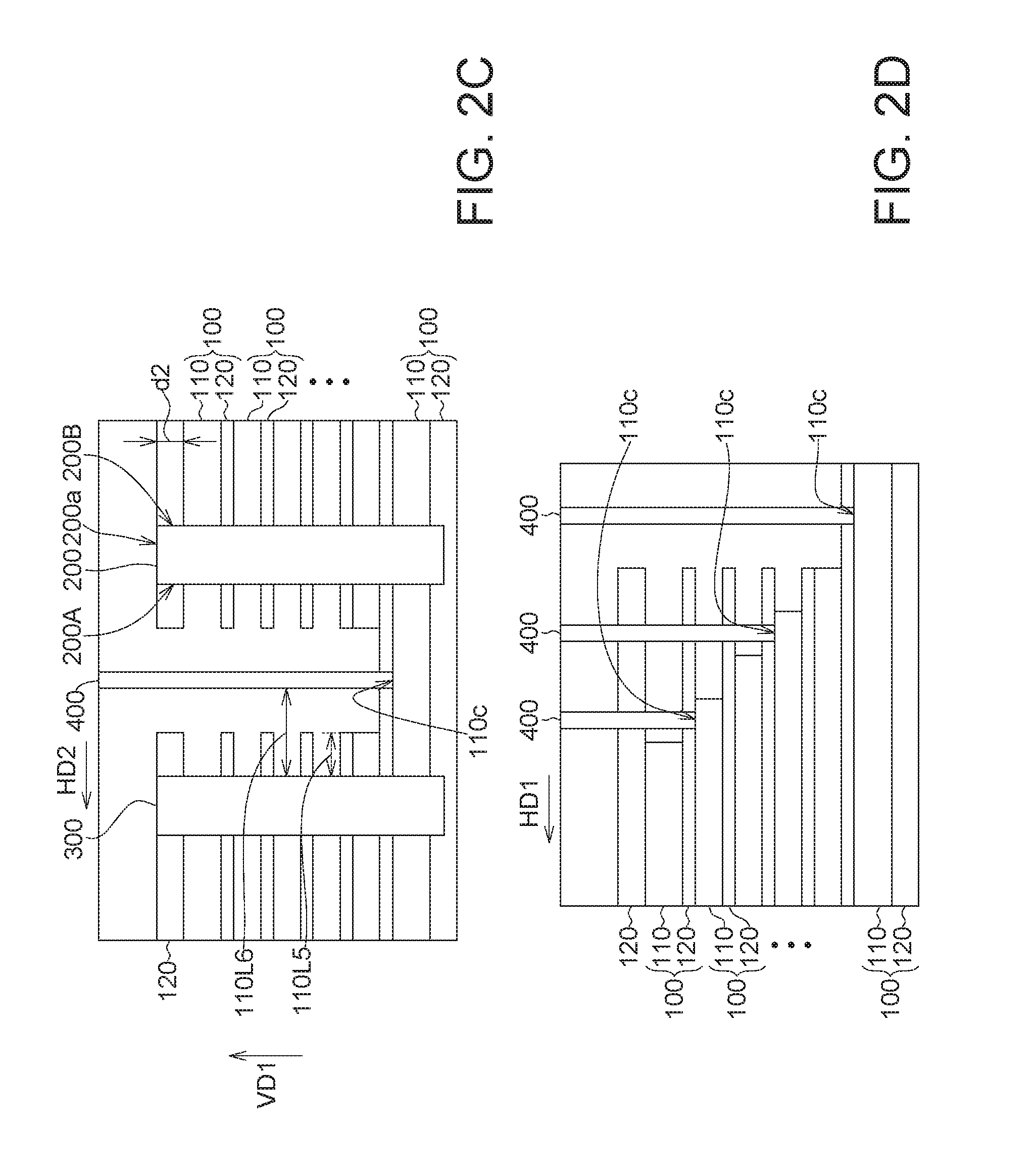
[0019] FIG. 1 shows a top view of a memory structure including stair contact structures according to an embodiment of the present disclosure, FIG. 2A shows a cross-sectional view along the cross-sectional line 2A-2A' in FIG. 1, FIG. 2B shows a cross-sectional view along the cross-sectional line 2B-2B' in FIG. 1, FIG. 2C shows a cross-sectional view along the cross-sectional line 2C-2C' in FIG. 1, and FIG. 2D shows a cross-sectional view along the cross-sectional line 2D-2D' in FIG. 1.
[0020] As shown in FIGS. 1 and 2A-2D, the memory structure 1 includes stair contact structures 10 and 20 and a memory array 30, and the memory array 30 is located between the stair contact structure 10 and the stair contact structure 20. In some embodiments, the memory array may include a plurality of memory blocks, for example, memory blocks 31 and 33; the stair contact structure 10 is, for example, a SSL contact pad region and may include a plurality of SSL contact pads 15; the stair contact structure 20 is, for example, a GSL contact pad region and may include a plurality of GSL contact pads 17; the memory array 30 is, for example, a 3D NAND memory array; but the present disclosure is not limited thereto.
[0021] In some embodiments, as shown in FIG. 1, the memory structure 1 may further have a trench 500 separating the stair contact structure 10 into two separate contact structures and separating the stair contact structure 20 into two separate contact structures. The two separate contact structures of each of the stair contact structure 10 and the stair contact structure 20 are respectively electrically connected to different memory blocks.
[0022] As shown in FIGS. 1 and 2A-2D, the stair contact structure 10/20 includes a plurality layers of stacking structures 100 and a first etch stop layer 200. Each stacking structure 100 includes a conductive layer 110 and an insulating layer 120, and the conductive layers 110 and the insulating layers 120 are interlaced. The first etch stop layer 200 penetrates through the stacking structures 100 vertically and extends along a first horizontal direction HD1. The conductive layers 110 of the stacking structures 100 located at a first sidewall 200A of the first etch stop layer 200 have a plurality of contact points 110c, and the contact points 110c are arranged along the first horizontal direction HD1 to form a stair structure having a plurality of stages.
[0023] In the embodiments, the material of the conductive layer 110 includes such as polysilicon, the material of the insulating layer 120 includes such as silicon oxide, and the material of the first etch stop layer 200 includes such as silicon nitride. In the embodiments, the topmost conductive layer 110 is electrically connected to such as the SSL contact pads 15 and/or the GSL contact pads 17, the bottommost conductive layer 110 is electrically connected to such as the inversion gate, and the conductive layers 110 in the middle are electrically connected to such as the word lines in the memory array 30.
[0024] According to the embodiments of the present disclosure, the contact points 110c of the conductive layers 110 in the stair contact structure 10/20 are arranged along the extending direction (i.e. the first horizontal direction HD1) of the first etch stop layer 200 to form a stair structure having a plurality of stages, such that the distance between the stair contact structure 10/20 and the memory array 30 can be reduced, and the effects of reduction of the overall size and area of the memory structure can be further achieved.
[0025] As shown in FIGS. 1 and 2A-2D, the stair contact structure 10/20 may further include a second etch stop layer 300. The second etch stop layer 300 penetrates through the stacking structures 100 vertically and extending along the first horizontal direction HD1. The aforementioned contact points 110c are located between the first etch stop layer 200 and the second etch stop layer 300.
[0026] According to the embodiments of the present disclosure, the contact points 110c of the conductive layers 110 in the stair contact structure 10/20 are arranged along the extending direction (i.e. the first horizontal direction HD1) of the first etch stop layer 200 to form a stair structure having a plurality of stages, and the contact points 110c are located between the first etch stop layer 200 and the second etch stop layer 300, such that the area occupied by the stair contact structure 10/20 is limited in the strip-shaped region between the first etch stop layer 200 and the second etch stop layer 300, and thus the size and area occupied by the stair contact structure 10/20 can be further reduced, and the effects of reduction of the overall size and area of the memory structure can be further achieved effectively.
[0027] According to some embodiments, the locations of the first etch stop layer 200 and the second etch stop layer 300 can be switched; in addition, when the stair contact structure 10/20 includes only the first etch stop layer 200 and does not include the second etch stop layer 300, the first etch stop layer 200 can be arranged at the location where the second etch stop layer 300 is located as shown in FIGS. 1. 2A and 2C.
[0028] In the embodiments, as shown in FIG. 1, the first etch stop layer 200 has a first length L1 along the first horizontal direction HD1, the stacking structures 100 have a second length L2 along the first horizontal direction HD1, and the second length L2 is larger than the first length L1.
[0029] In the embodiments, as shown in FIG. 1, the second etch stop layer 300 has a third length L3 along the first horizontal direction HD1, and the second length L2 of the stacking structures 100 is larger than the third length L3 of the second etch stop layer 300.
[0030] In the embodiments, as shown in FIGS. 2A and 2C, the first etch stop layer 200 has a second sidewall 200B opposite to the first sidewall 200A, the first etch stop layer 200 has a top surface 200a, the top surface 200a is kept apart from one contact point 110c of the plurality of contact points 110c by a first distance d1, the top surface 200a is kept apart from the topmost conductive layer 110 of the conductive layers 110 located at the second sidewall 200B of the first etch stop layer 200 by a second distance d2, and the first distance d1 is larger than the second distance d2.
[0031] In the embodiments, as shown in FIGS. 1, 2A and 2C, the conductive layers 110 located between the first etch stop layer 200 and the second etch stop layer 300 have a plurality of lengths along a second horizontal direction HD2, the second horizontal direction HD2 is perpendicular to the first horizontal direction HD1, and the lengths of the conductive layers 110 are different.
[0032] In some embodiments, the lengths 110L1-110L6 of the conductive layers 110 increase downwards along a vertical direction VD1, and the vertical direction VD1 is perpendicular to the first horizontal direction HD1 and the second horizontal direction HD2. For example, as shown in FIG. 2A, the lengths 110L1, 110L2, 110L3 and 110L4 of the conductive layers 110 increase downwards along the vertical direction VD1; as shown in FIG. 2C0, the lengths 110L5 and 110L6 of the conductive layers 110 increase downwards along the vertical direction VD1.
[0033] In the embodiments, as shown in FIGS. 1 and 2A-2D, the stair contact structure 10/20 may further include a plurality of conductive lines 400, and each conductive line 400 is electrically connected to each contact point 113c.
[0034] FIG. 3A shows a top view of a memory structure including stair contact structures according to another embodiment of the present disclosure, and FIG. 3B shows a cross-sectional view along the cross-sectional line 3B-3B' in FIG. 3A. The elements in the present embodiment sharing similar or the same labels with those in the previous embodiment are similar or the same elements, and the description of which is omitted.
[0035] As shown in FIGS. 3A-3B, the memory structure 2 includes a first stair contact structure 11, a second stair contact structure 13, a first memory block 31 and a second memory block 33. The first stair contact structure 11 and the second stair contact structure 13 are separated from each other by a trench 500. The first memory block 31 and the second memory block 33 are respectively electrically connected to the first stair contact structure 11 and the second stair contact structure 13. In the embodiments, the two sets of the first stair contact structure 11 and the second stair contact structure 13 form the stair contact structure 10 and the stair contact structure 20, respectively, the first memory block 31 and the second memory block 33 form the memory array 30, and the memory array 30 is located between the stair contact structure 10 and the stair contact structure 20. In some embodiments, the stair contact structure 10 is, for example, a SSL contact pad region and may include a plurality of SSL contact pads 15; the stair contact structure 20 is, for example, a GSL contact pad region and may include a plurality of GSL contact pads 17; the memory array 30 is, for example, a 3D NAND memory array; but the present disclosure is not limited thereto.
[0036] The first stair contact structure 11 and the second stair contact structure 13 respectively includes a plurality layers of stacking structures 100, each stacking structure 100 includes a conductive layer 110 and an insulating layer 120, and the conductive layers 110 and the insulating layers 120 are interlaced. The conductive layers 110 of the first stair contact structure 11 have a plurality of first contact points 110c1, the conductive layers 110 of the second stair contact structure 13 have a plurality of second contact points 110c2, the first contact points 110c1 and second contact points 110c2 are arranged respectively along a first direction D1 and a second direction D2 to form a first stair structure S1 and a second stair structure S2 having a plurality of stages, and the first direction D1 is different from the second direction D2.
[0037] In the embodiments, as shown in FIG. 3B, the conductive layers 110 in the first stair contact structure 11 have a plurality of lengths along the first direction D1, and the lengths of the conductive layers 110 increase downwards along the vertical direction VD1. In the embodiments, as shown in FIG. 3B, the conductive layers 110 in the second stair contact structure 13 have a plurality of lengths along the second direction D2, and the lengths of the conductive layers 110 increase downwards along the vertical direction VD1.
[0038] For example, as shown in FIG. 3B, the lengths L1a, L1b, L1c, L1d, L1e and L1f of the conductive layers 110 in the first stair contact structure 11 increase downwards along the vertical direction VD1, and the lengths L2a, L2b, L2c, Ltd, L2e and L2f of the conductive layers 110 in the second stair contact structure 13 increase downwards along the vertical direction VD1.
[0039] In the embodiments, as shown in FIGS. 3A-3B, the conductive layers 110 of the first stair contact structure 11 have a plurality of first notches 130a-130e, the conductive layers 110 of the second stair contact structure 13 have a plurality of second notches 140a-140e, and the sizes of the first notches 130a-130e and the sizes of the second notches 140a-140e decrease downwards along the vertical direction VD1.
[0040] In the embodiments, as shown in FIGS. 3A-3B, the memory structure 2 may further include a plurality of conductive lines 400. Each conductive line 400 is correspondingly electrically connected to each first contact point 110c1 or each second contact point 110c2.
[0041] In some embodiments, referring to FIGS. 1, 2A and 2C, the first stair contact structure 11 of the memory structure 2 in the present embodiment may further include a first etch stop layer (not shown in FIGS. 3A-3B) as well, the first etch stop layer may penetrate through the stacking structures 100 of the first stair contact structure 11 vertically and extend along the first horizontal direction HD1, and the first contact points 110c1 are located at a first sidewall of the first etch stop layer, as shown in FIGS. 1, 2A and 2C.
[0042] In some other embodiments (not shown in FIGS. 3A-3B, referring to FIGS. 1, 2A and 2C, the first stair contact structure 11 of the memory structure 2 in the present embodiment may further include a second etch stop layer as well, the second stair contact structure 13 of the memory structure 2 in the present embodiment may also include a first etch stop layer and/or a second etch stop layer, and of which the arrangements can be referred to FIGS. 1, 2A and 2C and the description is omitted.
[0043] FIG. 4A to FIG. 18B show a flow chart of a manufacturing method of a memory structure including stair contact structures according to an embodiment of the present disclosure. The elements in the present embodiment sharing similar or the same labels with those in the previous embodiments are similar or the same elements, and the description of which is omitted.
[0044] FIG. 4A shows a top view of the present step, and FIG. 4B shows a cross-sectional view along the cross-sectional line 4B-4B' in FIG. 4A. As shown in FIGS. 4A-4B, a plurality layers of stacking structures 100 are formed, each stacking structure 100 includes a conductive layer 110 and an insulating layer 120, and the conductive layers 110 and the insulating layers 120 are interlaced.
[0045] FIG. 5A shows a top view of the present step, and FIG. 5B shows a cross-sectional view along the cross-sectional line 5B-5B' in FIG. 5A. As shown in FIGS. 5A-5B, a patterned photoresist PR is formed on the stacking structures 100, and the patterned photoresist PR has an opening 600. In the embodiment, the opening 600 is located such as at the center of the cross-sectional line 5B-5B'.
[0046] Next, please refer to FIGS. 6A-16B, the stacking structures 100 are etched N times by using the patterned photoresist PR as a mask, and N is a positive integer. Each time of etching the stacking structures 100 includes performing a dry etching process on the stacking structures 100 and performing an isotropic etching process on the stacking structures 100. In etch time of performing the dry etching process on the stacking structures 100, a thickness of one layer of a portion of the stacking structures 100 is etched away, and in etch time of performing the isotropic etching process on the stacking structures 100, a width of one conductive layer 110 or multiple conductive layers 110 of the stacking structures 100 is trimmed off. The detailed manufacturing process includes such as the following steps.
[0047] FIG. 6A shows a top view of the present step, and FIG. 6B shows a cross-sectional view along the cross-sectional line 6B-6B' in FIG. 6A. As shown in FIGS. 6A-6B, a dry etching process is performed on the stacking structures 100 by using the patterned photoresist PR as a mask, and a thickness T1 of one layer is etched away. As shown in FIGS. 6A-6B, an area of the region 100a of the portion of the stacking structures 100 of which a thickness T1 of one layer is etched away is substantially the same with an area of the opening 600 of the patterned photoresist PR. The term "substantially the same" indicates almost or approximately the same and may include size variance within the manufacturing processing tolerance.
[0048] FIG. 7A shows a top view of the present step, and FIG. 7B shows a cross-sectional view along the cross-sectional line 7B-7B' in FIG. 7A. As shown in FIGS. 7A-7B, an isotropic etching process is performed on the stacking structures 100 by using the patterned photoresist PR as a mask to trim off a width W1 of one conductive layer 110 or multiple conductive layers 110 of the stacking structures 100. In the embodiments, the isotropic etching process provides a high etching selectivity of the material of the conductive layers 110 to the material of the insulating layers 120; that is, only the conductive layers 110 are partially laterally etched, and the insulating layers 120 are not etched, such that the insulating layers 120 are provided with effects of etching protection for protecting other conductive layers 110 located underneath from being damaged by the isotropic etching process, and only the exposed conductive layers 110 are laterally partially etched away. The laterally etched conductive layers 110 have an opening, and the region 100b of the opening is equal to the enlarged range of the aforementioned region 100a extended outwards omnidirectionally by a width W1. In the embodiments, the isotropic etching process may be a dry etching process or a wet etching process.
[0049] In the embodiments, after every time the stacking structures 100 is etched, the thickness of the patterned photoresist PR may be reduced by the consumption from the etching process. As shown in FIGS. 6B and 7B, the patterned photoresist PR is apparently thinned.
[0050] As shown in FIGS. 6A-7B, one time of etching the stacking structures 100 by using the patterned photoresist PR as a mask is completed (i.e. one time of the dry etching process plus one time of the isotropic etching process), and the aforementioned N equals to 1. Below the step of etching the stacking structures 100 will repeat multiple times.
[0051] FIG. 8A shows a top view of the present step, and FIG. 8B shows a cross-sectional view along the cross-sectional line 8B-8B' in FIG. 8A. As shown in FIGS. 8A-8B, a dry etching process is performed on the stacking structures 100 by using the patterned photoresist PR as a mask, and a thickness T1 of one layer is etched away. In the present embodiment, the same thickness T1 being etched away in each time of the dry etching process is taken as an example; in other embodiments, the thicknesses etched away by multiple dry etching processes can be different and varied/adjusted according to actual needs.
[0052] FIG. 9A shows a top view of the present step, and FIG. 9B shows a cross-sectional view along the cross-sectional line 9B-9B' in FIG. 9A. As shown in FIGS. 9A-9B, an isotropic etching process is performed on the stacking structures 100 by using the patterned photoresist PR as a mask, and a width W2 of two conductive layers 110 of the stacking structures 100 is trimmed off. In the embodiments, the width W2 may be the same with or different from the width W2 trimmed off in the previous isotropic etching process. The two conductive layers 110 laterally etched both have openings; the opening of the conductive layer 110 laterally etched one time has the region 100b, the opening of the conductive layer 110 laterally etched two times has a region 100c, and the region 100c is equal to the enlarged range of the aforementioned region 100b extended outwards omnidirectionally by a width W2.
[0053] As shown in FIGS. 8A-9B, two times of etching the stacking structures 100 by using the patterned photoresist PR as a mask are completed, and the aforementioned N equals to 2. In addition, as shown in FIGS. 8B and 9B, the patterned photoresist PR is apparently further thinned.
[0054] FIG. 10A shows a top view of the present step, and FIG. 10B shows a cross-sectional view along the cross-sectional line 10B-10B' in FIG. 10A. As shown in FIGS. 10A-10B, a dry etching process is performed on the stacking structures 100 by using the patterned photoresist PR as a mask, and a thickness T1 of one layer is etched away.
[0055] FIG. 11A shows a top view of the present step, and FIG. 11B shows a cross-sectional view along the cross-sectional line 11B-11B' in FIG. 11A. As shown in FIGS. 11A-11B, an isotropic etching process is performed on the stacking structures 100 by using the patterned photoresist PR as a mask, and a width W3 of three conductive layers 110 of the stacking structures 100 is trimmed off. The three conductive layers 110 laterally etched all have openings; the opening of the conductive layer 110 laterally etched one time has the region 100b, the opening of the conductive layer 110 laterally etched two times has the region 100c, the opening of the conductive layer 110 laterally etched three times has a region 100d, and the region 100d is equal to the enlarged range of the aforementioned region 100c extended outwards omnidirectionally by a width W3.
[0056] As shown in FIGS. 10B and 11B, the patterned photoresist PR is apparently further thinned. In some embodiments, after etching every M times the stacking structures 100, M being a positive integer and smaller than N (i.e. the manufacturing process is not fully completed), the thickness of the patterned photoresist PR is thinned. The manufacturing method according to the present disclosure may further include the following steps: forming a supplementary patterned photoresist on the stacking structures 100, the pattern of the supplementary patterned photoresist is the same as the pattern of the original patterned photoresist PR, and the supplementary patterned photoresist is disposed on the original patterned photoresist PR.
[0057] For example, as shown in FIGS. 12A-12B (FIG. 12A shows a top view of the present step, and FIG. 12B shows a cross-sectional view along the cross-sectional line 12B-12B' in FIG. 12A), the supplementary patterned photoresist PR1 is disposed on the stacking structures 100, the pattern of the supplementary patterned photoresist PR is the same as the pattern of the patterned photoresist PR, and the supplementary patterned photoresist PR1 is disposed on the original patterned photoresist PR. In the present embodiment, the supplementary patterned photoresist being formed after the stacking structures 100 being etched three times (M=3) is taken as an example; however, the value of M can be larger than 3, for example, 5 to 10, but the present disclosure is not limited thereto.
[0058] FIG. 13A shows a top view of the present step, and FIG. 13B shows a cross-sectional view along the cross-sectional line 13B-13B' in FIG. 13A. As shown in FIGS. 13A-13B, a dry etching process is performed on the stacking structures 100 by using the patterned photoresist PR and optionally the supplementary patterned photoresist PR1 having the same pattern with that of the patterned photoresist PR as a mask, and a thickness T1 of one layer is etched away.
[0059] FIG. 13A shows a top view of the present step, and FIG. 13B shows a cross-sectional view along the cross-sectional line 13B-13B' in FIG. 13A. As shown in FIGS. 13A-13B, an isotropic etching process is performed on the stacking structures 100 by using the patterned photoresist PR (and the supplementary patterned photoresist PR1 having the same pattern with that of the patterned photoresist PR) as a mask, and a width W4 of four conductive layers 110 of the stacking structures 100 is trimmed off. The four conductive layers 110 laterally etched all have openings; the opening of the conductive layer 110 laterally etched one time has the region 100b, the opening of the conductive layer 110 laterally etched two times has the region 100c, the opening of the conductive layer 110 laterally etched three times has the region 100d, the opening of the conductive layer 110 laterally etched four times has a region 100e, and the region 100e is equal to the enlarged range of the aforementioned region 100d extended outwards omnidirectionally by a width W4.
[0060] FIG. 15A shows a top view of the present step, and FIG. 15B shows a cross-sectional view along the cross-sectional line 15B-15B' in FIG. 15A. As shown in FIGS. 15A-15B, a dry etching process is performed on the stacking structures 100 by using the patterned photoresist PR and optionally the supplementary patterned photoresist PR1 having the same pattern with that of the patterned photoresist PR as a mask, and a thickness T1 of one layer is etched away.
[0061] In the present disclosure, the stacking structures 100 being etched four times (N=4) is taken as an example; however, the value of N may be larger than 4, and the present disclosure is not limited thereto.
[0062] As shown in FIGS. 16A-16B (FIG. 16A shows a top view of the present step, and FIG. 16B shows a cross-sectional view along the cross-sectional line 16B-16B' in FIG. 16A), the patterned photoresist PR is removed. The patterned photoresist being removed herein indicates the original patterned photoresist PR and one or more than one supplementary patterned photoresists formed in the manufacturing process. In addition, as shown in FIGS. 16A-16B, an insulating layer 130 is formed on the stacking structures 100 and filled in the space between the insulating layers 120. The materials of the insulating layers 120 and the insulating layer 130 may be the same or different, and the structure of the insulating layers 120 are represented by dashed lines in FIG. 16B.
[0063] As shown in FIGS. 16A-16B, the conductive layers 110 of the stacking structures 100 have multiple contact points, and these contact points are arranged along a horizontal direction to form a stair structure having a plurality of stages. For example, the first contact points 110c1 are arranged along a first direction D1 to form a first stair structure S1 having a plurality of stages, and the second contact points 110c2 are arranged along a second direction D2 to form a second stair structure S2 having a plurality of stages.
[0064] Next, as shown in FIGS. 17A-17B (FIG. 17A shows a top view of the present step, and FIG. 17B shows a cross-sectional view along the cross-sectional line 17B-17B' in FIG. 17A), a memory array 30 is manufactured. In the embodiments, the memory array 30 may include two memory blocks 31 and 33.
[0065] As shown in FIGS. 17A-17B, the stacking structures 100 are etched for forming a trench 500, and the trench 500 separates the stacking structures 100 into two separate contact structures, for example, the first stair contact structure 11 and the second stair contact structure 13, and the first stair contact structure 11 and the second stair contact structure 13 are respectively electrically connected to the memory block 31 and the memory block 33. According to the embodiments of the present disclosure, the whole stair structure formed by the aforementioned N times of etching processes is further divided into two separate stair contact structures by the trench 500, such that two stair contact structures that can be respectively electrically connected to two separate memory blocks can be formed in one manufacturing process; as such, the manufacturing process can be simplified, the area of the region occupied by one stair contact structure can be reduced, and meanwhile one stair contact structure can be correspondingly electrically connected to a smaller memory block, which can reduce the number of memory units in one erase operation.
[0066] Next, as shown in FIGS. 18A-18B (FIG. 18A shows a top view of the present step, and FIG. 18B shows a cross-sectional view along the cross-sectional line 18B-18B' in FIG. 18A), a plurality of conductive lines 400 are disposed, and each conductive line 400 is electrically connected to each contact point 110c1/110c2. As such, the memory structure 2 and of which the stair contact structures as shown in FIGS. 3A-3B is formed.
[0067] In conventional manufacturing process, the formation of each contact point located in each different level (stage) requires a photo mask step and an etching process, thus the manufacturing process is more complex and difficult, and a higher manufacturing cost is required. On the contrary, according to the embodiments of the present disclosure, the stair contact structure can be made by multiple etching processes with fewer mask steps, such that the manufacturing process is simplified, costs are reduced, and the manufacturing time is reduced; in addition, the manufacturing process of the present disclosure can be integrated into the existing semiconductor manufacturing process, thereby can be applied in the manufacturing processes for various 3D high-density memory devices.
[0068] FIG. 19 to FIG. 25B show a flow chart of a manufacturing method of a memory structure including stair contact structures according to another embodiment of the present disclosure. The elements in the present embodiment sharing similar or the same labels with those in the previous embodiment are similar or the same elements, and the description of which is omitted. It is to be noted that the present embodiment describes the manufacturing method of one stair contact structure of the memory structure as shown in FIGS. 1 and 2A-2D.
[0069] FIG. 19 shows a top view of the present step, FIG. 19A shows a cross-sectional view along the cross-sectional line 19A-19A' in FIG. 19, and FIG. 19B shows a cross-sectional view along the cross-sectional line 19B-19B' in FIG. 19. As shown in FIGS. 19-19B, a plurality of stacking structures 100 are formed, each stacking structure 100 includes a conductive layer 110 and an insulating layer 120, and the conductive layers 110 and the insulating layers 120 are interlaced.
[0070] Next, as shown in FIGS. 20-20B (FIG. 20 shows a top view of the present step, FIG. 20A shows a cross-sectional view along the cross-sectional line 20A-20A in FIG. 20, arid FIG. 20B shows a cross-sectional view along the cross-sectional line 20B-20B' in FIG. 20), before forming the patterned photoresist PR on the stacking structures 110, a first etch stop layer 200 is formed, the first etch stop layer 200 penetrates through the stacking structures 100 vertically and extends along a first horizontal direction HD1, and the first etch stop layer 200 has a first sidewall 200A.
[0071] As shown in FIGS. 20-20B, before forming the patterned photoresist PR on the stacking structures 100, a second etch stop layer 300 may be further formed, and the second etch stop layer 300 penetrates through the stacking structures 100 vertically and extends along the first horizontal direction HD1.
[0072] Next, as shown in FIGS. 21-21B (FIG. 21 shows a top view of the present step, FIG. 21A shows a cross-sectional view along the cross-sectional line 21A-21A' in FIG. 21, and FIG. 21B shows a cross-sectional view along the cross-sectional line 21 B-21 B' in FIG. 21), the patterned photoresist PR is formed on the stacking structures 100, and the patterned photoresist PR has an opening 600.
[0073] Next, as shown in FIGS. 22-22B (FIG. 22 shows a top view of the present step, FIG. 22A shows a cross-sectional view along the cross-sectional line 22A-22A' in FIG. 22, and FIG. 22B shows a cross-sectional view along the cross-sectional line 22B-22B' in FIG. 22), a dry etching process is performed on the stacking structures 100 by using the patterned photoresist PR as a mask to etch away a thickness T1 of one layer, and then an isotropic etching process is performed on the stacking structures 100 by using the patterned photoresist PR as a mask to trim off a width W1 of one conductive layer 110 of the stacking structures 100. The area of the region 100a of the portion of the stacking structures 100 of which a thickness T1 of one layer is etched away is substantially the same with the area of the opening 600 of the patterned photoresist PR. The region 100b of the opening of the laterally etched conductive layer 110 is equal to the enlarged range of the aforementioned region 100b extended outwards omnidirectionally by a width W1.
[0074] Next, as shown in FIGS. 23-23B (FIG. 23 shows a top view of the present step, FIG. 23A shows a cross-sectional view along the cross-sectional line 23A-23A in FIG. 23, and FIG. 23B shows a cross-sectional view along the cross-sectional line 23B-23B' in FIG. 23), a dry etching process and then an isotropic etching process are continuously performed on the stacking structures 100 by using the patterned photoresist PR as a mask. Since the first etch stop layer 200 is disposed at a location separated from the region 100a by a distance of the width W1, the present isotropic etching process stops at the first sidewall 200A of the first etch stop layer 200, and the present isotropic etching process trims off the a width W2 of two conductive layers 110 of the stacking structures 100 towards other directions. The opening of the conductive layer 110 laterally etched two times has a region 100c, and the region 100c is equal to the enlarged range of the aforementioned region 100b extended outwards by a width W2 except towards the first etch stop layer 200.
[0075] Next, as shown in FIGS. 24-24B (FIG. 24 shows a top view of the present step, FIG. 24A shows a cross-sectional view along the cross-sectional line 24A-24A in FIG. 24, and FIG. 24B shows a cross-sectional view along the cross-sectional line 24B-24B' in FIG. 24), a dry etching process and then an isotropic etching process are continuously performed on the stacking structures 100 by using the patterned photoresist PR as a mask. Since the first etch stop layer 200 is disposed at a location separated from the region 100a by a distance of the width W1, and the second etch stop layer 300 is disposed at a location separated from the region 100c by a distance less than the width W3, the present isotropic etching process stops at the first sidewall 200A of the first etch stop layer 200 and the first sidewall 300A of the second etch stop layer 300, the present isotropic etching process trims off the a width W3 of three conductive layers 110 of the stacking structures 100 towards other two directions, and the present isotropic etching process trims off the a width W3 of two conductive layers 110 and a width W3' of one conductive layer 110 of the stacking structures 100 towards the second etch stop layer 300. The opening of the conductive layer 110 laterally etched three times has a region 100d, and the region 100d is equal to the enlarged range of the aforementioned region 100c extended towards the second etch stop layer 300 by a width W3' and extended towards other two directions by a width W3 except towards the first etch stop layer 200.
[0076] Next, as shown in FIGS. 25-25B (FIG. 25 shows a top view of the present step, FIG. 25A shows a cross-sectional view along the cross-sectional line 25A-25A' in FIG. 25, and FIG. 25B shows a cross-sectional view along the cross-sectional line 25B-25B' in FIG. 25), a dry etching process and then an isotropic etching process are continuously performed on the stacking structures 100 by using the patterned photoresist PR as a mask. Since the first etch stop layer 200 is disposed at a location separated from the region 100a by a distance of the width W1, and the second etch stop layer 300 is disposed at a location separated from the region 100c by a distance less than the width W3, the present isotropic etching process stops at the first sidewall 200A of the first etch stop layer 200 and the first sidewall 300A of the second etch stop layer 300, and the present isotropic etching process trims off the a width W4 of four conductive layers 110 of the stacking structures 100 towards other two directions. The opening of the conductive layer 110 laterally etched four times has a region 100e, and the region 100e is equal to the enlarged range of the aforementioned region 100d extended towards two is directions by a width W4 except towards the first etch stop layer 200 and the second etch stop layer 300.
[0077] Next, please refer to FIGS. 1, 2A-2D and 16A-18B the patterned photoresist PR is removed, an insulating layer is formed on the stacking structures 100 and filled in the spaces between the insulating layers 120. As such, the conductive layers 110 of the stacking structures 100 have a plurality of contact points, and the contact points are arranged along the first horizontal direction HD1 to form a stair structure having a plurality of stages. The contact points are located at the first sidewall 200A of the first etch stop layer 200, and the contact points are located between the first etch stop layer 200 and the second etch stop layer 300. Next, conductive lines 400 are disposed, and each conductive line 400 is electrically connected to each contact point. As such, the stair contact structure as shown in FIGS. 1 and 2A-20 is formed.
[0078] According to the embodiments of the present disclosure, the stair contact structure can be manufactured by multiple etching processes with fewer mask steps, such that the manufacturing process is simplified, the cost is reduced, and the overall manufacturing time can be reduced as well. In addition, the first etch stop layer 200 and/or the second etch stop layer 300 disposed in the stacking structures 100 can not only further reduce the size of the stair contact structure 10/20 along the second horizontal direction HD2 but can also provide supports in the multiple etching processes, preventing the un-etched insulating layers 120 from being collapsed causing serious damages to the overall structure.
[0079] While the disclosure has been described by way of example and in terms of the exemplary embodiment(s), it is to be understood that the disclosure is not limited thereto. On the contrary, it is intended to cover various modifications and similar arrangements and procedures, and the scope of the appended claims therefore should be accorded the broadest interpretation so as to encompass all such modifications and similar arrangements and procedures.
* * * * *
D00000
D00001
D00002
D00003
D00004
D00005
D00006
D00007
D00008
D00009
D00010
D00011
D00012

D00013
D00014

D00015

D00016

D00017

D00018

D00019

D00020

D00021

D00022

D00023

D00024

D00025

D00026

D00027
D00028

D00029

D00030

D00031

D00032

D00033

D00034

D00035

D00036

D00037

D00038

D00039
D00040

D00041

D00042

D00043

D00044

D00045

D00046

D00047

D00048

D00049

XML
uspto.report is an independent third-party trademark research tool that is not affiliated, endorsed, or sponsored by the United States Patent and Trademark Office (USPTO) or any other governmental organization. The information provided by uspto.report is based on publicly available data at the time of writing and is intended for informational purposes only.
While we strive to provide accurate and up-to-date information, we do not guarantee the accuracy, completeness, reliability, or suitability of the information displayed on this site. The use of this site is at your own risk. Any reliance you place on such information is therefore strictly at your own risk.
All official trademark data, including owner information, should be verified by visiting the official USPTO website at www.uspto.gov. This site is not intended to replace professional legal advice and should not be used as a substitute for consulting with a legal professional who is knowledgeable about trademark law.