Battery Charger System
Lai; Zheren ; et al.
U.S. patent application number 16/039321 was filed with the patent office on 2019-04-18 for battery charger system. The applicant listed for this patent is TEXAS INSTRUMENTS INCORPORATED. Invention is credited to Zheren Lai, Ryan Erik Lind, Alexander Lee McHale, Jinrong Qian, Sai Bun Wong.
| Application Number | 20190115765 16/039321 |
| Document ID | / |
| Family ID | 66097564 |
| Filed Date | 2019-04-18 |


View All Diagrams
| United States Patent Application | 20190115765 |
| Kind Code | A1 |
| Lai; Zheren ; et al. | April 18, 2019 |
BATTERY CHARGER SYSTEM
Abstract
A system for charging a battery includes an adapter, and a charger coupled to receive power from the adapter, and to provide a charging current to the battery. The charger includes a power stage with a charge pump to provide the charging current, and a feedback circuit to provide a feedback signal to the adapter. The power stage can be one of: an adjustable current source with voltage clamp, and an adjustable voltage source with current clamp. The charge pump can be implemented as a voltage divider, so that an input adapter current is multiplied by a pre-defined divider ratio to provide the charging current. The charge pump can be one of: single-phase; and multi-phase.
| Inventors: | Lai; Zheren; (Plano, TX) ; Qian; Jinrong; (Plano, TX) ; Wong; Sai Bun; (Irving, TX) ; Lind; Ryan Erik; (Knoxville, TN) ; McHale; Alexander Lee; (Knoxville, TN) | ||||||||||
| Applicant: |
|
||||||||||
|---|---|---|---|---|---|---|---|---|---|---|---|
| Family ID: | 66097564 | ||||||||||
| Appl. No.: | 16/039321 | ||||||||||
| Filed: | July 18, 2018 |
Related U.S. Patent Documents
| Application Number | Filing Date | Patent Number | ||
|---|---|---|---|---|
| 62533797 | Jul 18, 2017 | |||
| Current U.S. Class: | 1/1 |
| Current CPC Class: | H02J 7/02 20130101; G05F 1/575 20130101; H02J 7/008 20130101; H02J 7/00 20130101; H02M 3/07 20130101; H02J 2207/20 20200101 |
| International Class: | H02J 7/00 20060101 H02J007/00; H02M 3/07 20060101 H02M003/07 |
Claims
1. A system for charging a battery, comprising: an adapter; a charger coupled to receive power from the adapter, and to provide a charging current to the battery; the charger including a power stage with: a charge pump to provide the charging current, and a feedback circuit to provide a feedback signal to the adapter.
2. The system of claim 1, wherein the power stage is one of: an adjustable current source with voltage clamp, and an adjustable voltage source with current clamp. voltage source adapter>current depends on device current input voltage div 2, batt voltage div by impedance adjustable voltage>current source adapter>push current typical adapter technology>v source with I clamp>v source provides current up to I clamp.
3. The system of claim 1, wherein the charge pump comprises a voltage divider.
4. The system of claim 3, wherein the charge pump voltage divider multiplies input adapter current by a pre-defined divider ratio to provide the charging current.
5. The system of claim 1, wherein the charge pump comprises one of: single-phase; and multi-phase.
Description
CROSS-REFERENCE TO RELATED APPLICATIONS
[0001] Priority is claimed under 37 CFR 1.78 and 35 USC 119(e) to U.S. Provisional Application 62/533,797 (Docket TI-77696PS), filed 2017 Jul. 18, and U.S. Provisional Application 62/647,809 (Docket TI-77696PS1), filed 2018 Mar. 25, each of which is incorporated by reference in its entirety.
BACKGROUND
[0002] Battery charging systems provide charging current to battery-powered devices, such as mobile phones. Device batteries are increasing in both size and supported charging rates. A 3,000-mAh battery can be capable of charging at 6 A, but charger efficiency--and consequently, the power dissipated in the phone--can be a limiting factor to charging at this rate.
[0003] Rapid-charging power adapters can designed to provide high charging currents, although disadvantages of current rapid charging solutions can include: (a) expensive cabling from the adapter; (b) large inductors; and (c) significant power dissipation.
BRIEF SUMMARY
[0004] This Brief Summary is provided as a general introduction to the Disclosure provided by the Detailed Description and Drawings, summarizing aspects and features of the Disclosure. It is not a complete overview of the Disclosure, and should not be interpreted as identifying key elements or features of, or otherwise characterizing or delimiting the scope of, the disclosed invention.
[0005] The Disclosure describes apparatus and methods for a switched-capacitor current multiplication battery charger architecture.
[0006] According to aspects of the Disclosure, a system for charging a battery includes an adapter, and a charger coupled to receive power from the adapter, and to provide a charging current to the battery. The charger includes a power stage with a charge pump to provide the charging current, and a feedback circuit to provide a feedback signal to the adapter. The power stage can be one of: an adjustable current source with voltage clamp, and an adjustable voltage source with current clamp. The charge pump can be implemented as a voltage divider, so that an input adapter current is multiplied by a pre-defined divider ratio to provide the charging current. The charge pump can be one of: single-phase; and multi-phase.
[0007] Other aspects and features of the invention claimed in this Patent Document will be apparent to those skilled in the art from the following Disclosure.
BRIEF DESCRIPTION OF THE DRAWINGS
[0008] FIGS. 1A and 1B illustrate an example battery charge system 1 that includes a power adapter 2 coupled over a bus 4 to a device (such as a mobile phone) that includes a switched-capacitor current multiplication battery charger 10 according to the Disclosure.
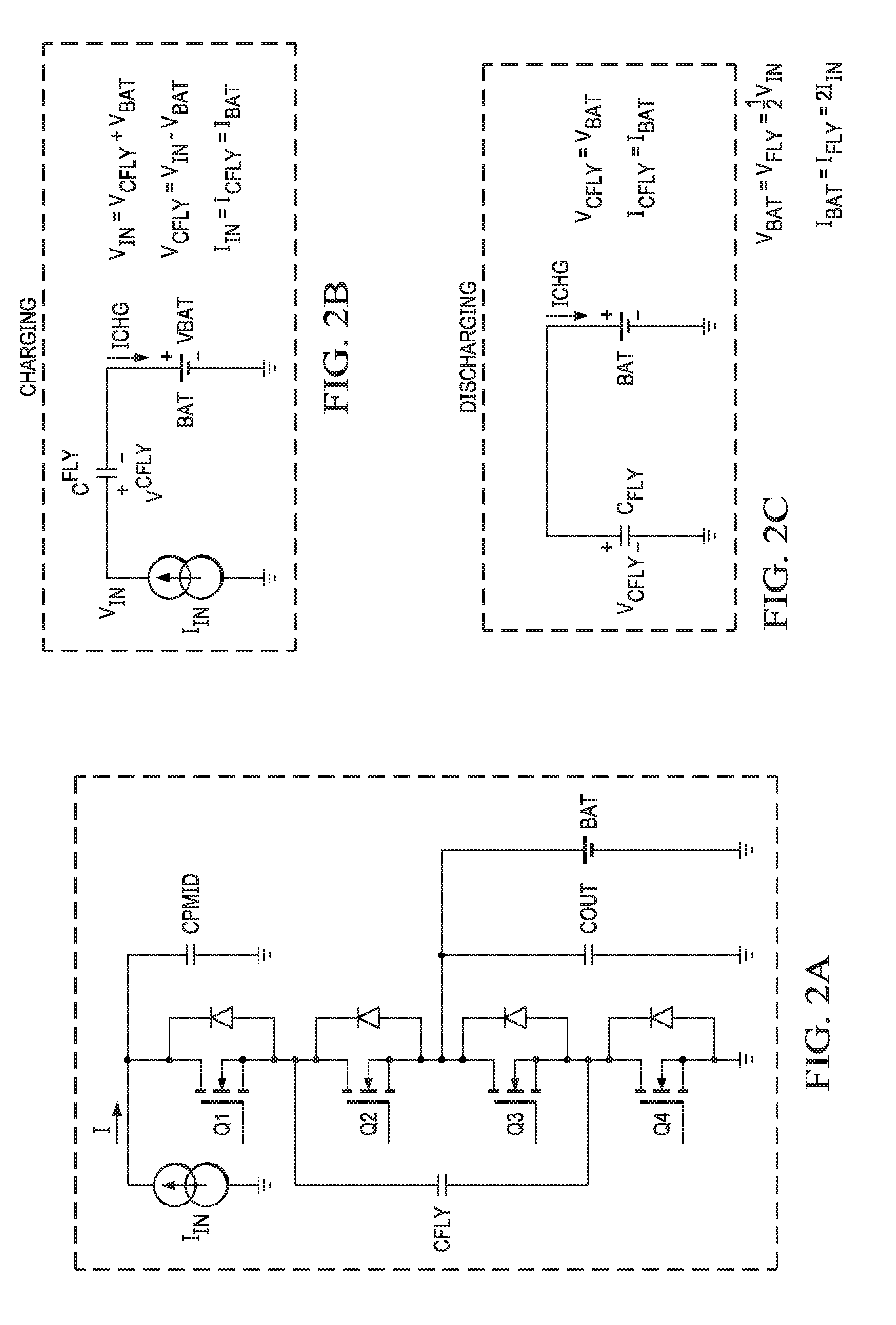
[0009] FIGS. 2A-2C illustrate an example simplified switched-capacitor charge pump, along with the equations for voltage and current during charging and discharging of CFLY capacitors.
[0010] FIG. 3A illustrates example waveforms for battery current and voltage. FIGS. 3B-3C illustrate circuit models with equivalent series resistance of CFLY, as well as the resistances of the switches Q1-Q4.
[0011] FIGS. 4A-4B illustrate an example switched-capacitor current multiplication battery charger with a constant current source, including representative V(CFLY) and I(CFLY) waveforms.
[0012] FIGS. 5A and 5B illustrate example efficiency curves for: FIG. 5A four CFLY capacitors per phase; and FIG. 5B three CFLY capacitors per phase.
[0013] FIG. 6 illustrates an example battery-charger profile for a switched-capacitor current multiplication architecture according to the Disclosure.
[0014] FIG. 7 is an example flow diagram illustrating switched-capacitor current multiplication batter charging according to the Disclosure.
[0015] FIGS. 8A and 8B provide example plots illustrating example charge-cycle data and example total charge-time data.
[0016] FIGS. 9A and 9B illustrates an example switched-capacitor current multiplication battery charger 20 according to the Disclosure, configured with a dual power stage (power phase).
[0017] FIGS. 10A and 10B provide example plots illustrating improvements in efficiency and ripple performance for multi-phase configurations.
[0018] FIGS. 11A and 11B illustrate an example battery charge system board implementation, such as for a mobile phone, including a dual-phase switched-capacitor current multiplication battery charger 30 according to the Disclosure, with FIG. 11B illustrating example system load.
DETAILED DESCRIPTION
[0019] This Description and the Drawings constitute a Disclosure for a switched-capacitor current multiplication (charge pump) battery charger architecture, including describing design examples (example implementations), and illustrating various technical features and advantages.
[0020] In brief overview, a switched-capacitor current multiplication (charge pump) battery charger system includes an adapter, and a charger coupled to receive power from the adapter, and to provide a charging current to the battery. The charger includes a power stage with a charge pump to provide the charging current, and a feedback circuit to provide a feedback signal to the adapter. The power stage can be one of: an adjustable current source with voltage clamp, and an adjustable voltage source with current clamp. The charge pump can be implemented as a voltage divider, so that an input adapter current is multiplied by a pre-defined divider ratio to provide the charging current. The charge pump can be one of: single-phase; and multi-phase.
[0021] FIGS. 1A and 1B illustrate an example battery charge system 1 that includes a power adapter 2 coupled over a bus 4 to a device (such as a mobile phone) that includes a switched-capacitor current multiplication battery charger 10 according to the Disclosure (sometimes referred to as a current multiplication battery charger or battery charger). Adapter 2 is configured to provide to the batter charger controlled power based on battery voltage and current, with feedback provided by the battery charger, such as a PPS (programmable power supply) wall adapter.
[0022] FIG. 1A illustrates the example switched-capacitor current multiplication battery charger 10, configured with a single power stage (power phase). A multi-phase/stage configuration is described in connection with FIGS. 9A/9B.
[0023] The switched-capacitor current multiplication battery charger 10 receives power from the adapter 2 (through transistor M1). The battery charger includes four switches Q1-Q4 controlled to alternately charge and discharge the flying (charge pump) capacitor CFLY. FIG. 1B illustrates example waveforms for V(BUS), V(BAT), I(BUS), I(BAT), and I(CFLY).
[0024] FIGS. 2A-2C illustrate an example simplified switched-capacitor charge pump, along with the equations for voltage and current during charging and discharging of CFLY capacitors.
[0025] In the charging phase (t.sub.1), Q1 and Q3 turn on and Q2 and Q4 turn off. This enables CFLY to be in series with the battery, where CFLY charges while delivering current to the battery. During the discharge phase (t.sub.2), Q1 and Q3 turn off and Q2 and Q4 turn on. During this time, the CFLY capacitor is parallel to the battery and provides charging current to it. The duty cycle is 50%, the battery current is half of the input voltage and the current delivered to the battery is twice the input current.
[0026] FIG. 3A illustrates example waveforms for battery current and voltage. FIGS. 3B-3C illustrate circuit models with equivalent series resistance of CFLY, as well as the resistances of the switches Q1-Q4.
[0027] FIGS. 4A-4B illustrate an example switched-capacitor current multiplication battery charger with a constant current source, including representative V(CFLY) and I(CFLY) waveforms. When using a constant current source, the CFLY current is constant while CFLY charges. If using a constant voltage source, the CFLY current follows the resistor-capacitor constant curve as shown in FIG. 4B. The effect of using a voltage source instead of a current source is to increase ripple current and RMS current, and to reduce efficiency due to higher conduction losses.
[0028] CFLY capacitor selection is an important design consideration. A recommended configuration includes two to four CFLY capacitors per phase. Additional CFLY capacitors can be used, but with diminishing returns, and at the expense of cost and board space.
[0029] Using fewer than four CFLY capacitors results in higher voltage and current ripple, and increased stress on each capacitor. The total effective capacitance should be 24 .mu.F or greater for optimal efficiency. Using four 22-.mu.F capacitors with a 10-V rating will achieve a 24-.mu.F capacitance, taking into account the bias voltage derating of the ceramic capacitors. A slower switching frequency can increase efficiency, but this also comes at the expense of high current ripple and increased stress on each capacitor.
[0030] FIGS. 5A and 5B illustrate example efficiency curves for: FIG. 5A four CFLY capacitors per phase; and FIG. 5B three CFLY capacitors per phase. The effect of the number of CFLY capacitors and switching frequency clearly evident.
[0031] Referring to FIG. 1A, the adapter 2 provides controlled voltage and current to the switched-capacitor current multiplication battery charger 10, with feedback from the battery charger based on sensed VBAT and IBAT. An example adapter is a PPS wall adapter. The USB PD specification has incorporated support for direct charge adapters with PPS. The PPS protocol enables switched capacitor chargers, while also supporting legacy USB 2.0, USB 3.1, USB Type-C current or BCS 1.2 voltage and currents.
[0032] The wall adapter (source) 2 preferably implements protection, without relying on the current multiplication battery charger 10 (sink). Similarly, the battery charger 10 preferably implements protection, without relying on the adapter (source). The adapter/source can also implement overcurrent protection.
[0033] For the switched-capacitor current multiplication battery charger architecture according to the Disclosure, the adapter/source should provide adjustable power based on the sink requirements. As an example, the source can be configured to adjust the output voltage in 20-mV increments and the current in 10-mA increments.
[0034] FIG. 6 illustrates an example battery-charger profile for a switched-capacitor current multiplication architecture according to the Disclosure. The switched-capacitor current multiplication architecture can be used with a battery-charger profile that includes pre-charge and final termination. The combination of an adapter source and a such a charger profile enables the system to accomplish the battery-charge profile shown in FIG. 6.
[0035] If the battery being charged is below a predefined voltage, such as 3.5 V, the charger is used during pre-charge and constant-current charging until reaching that predefined voltage. At that time, the battery charger 10 (device) provides feedback to the adapter/source (such as over a communication channel of a Type-C cable) to increase the voltage/current to meet pre-defined charging requirements (battery-charging profile).
[0036] Once the battery voltage reaches a voltage near the final charging voltage, the adapter reduces the voltage/current in small increments to prevent a battery overvoltage condition.
[0037] Once the PPS reduces the voltage/current so that the charging current is below the undercurrent threshold for the switched-capacitor device, charging stops and charging can resume according to a predefined battery-charging profile for current tapering and final termination.
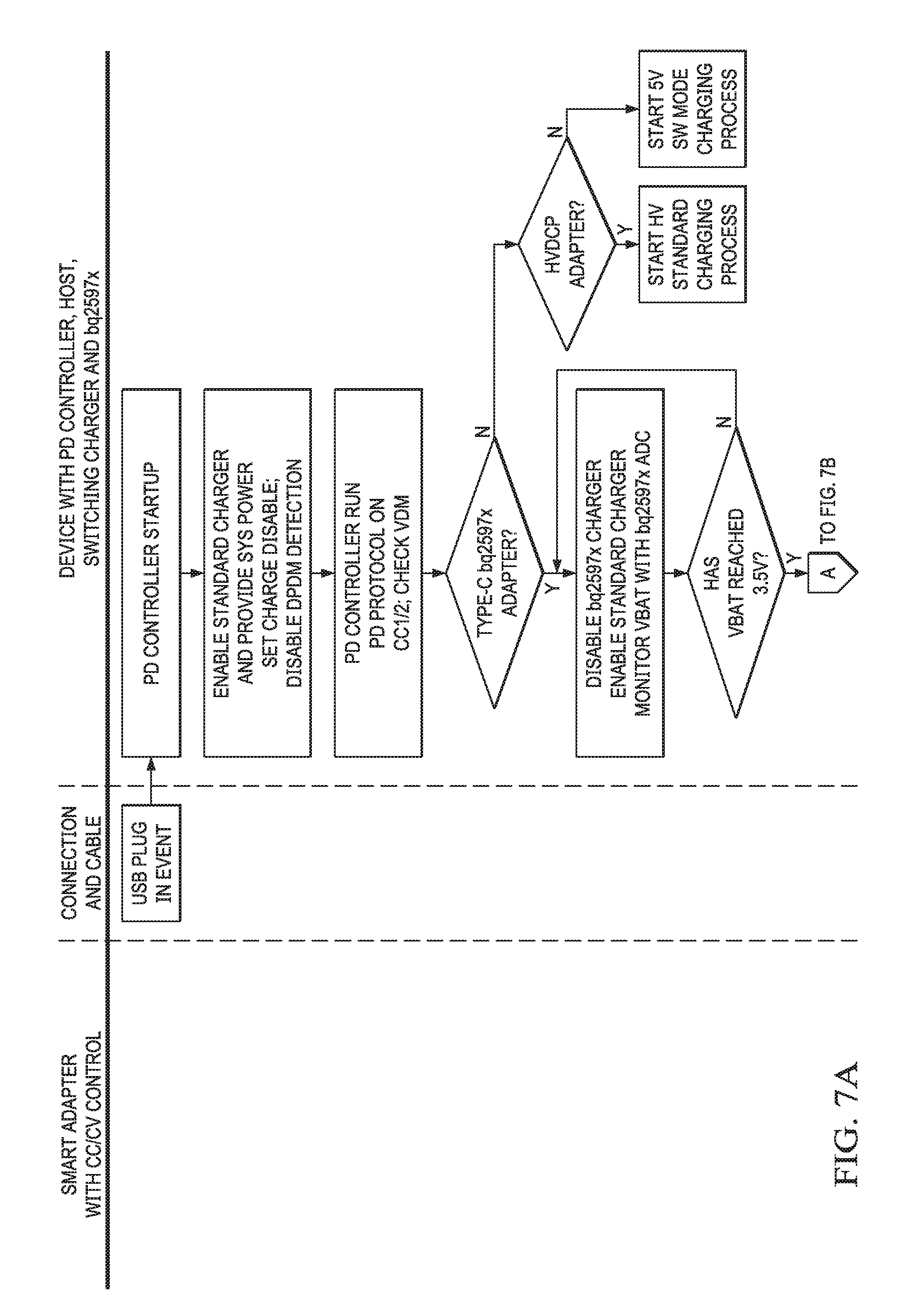
[0038] FIG. 7 is an example flow diagram illustrating switched-capacitor current multiplication batter charging according to the Disclosure. Referring also to FIG. 1A, initially, 5 V is present on the bus 4, which is then negotiated depending on the capabilities and state of the adapter/sink. The example battery-charging flow is as follows. The adapter 2 is configured as an example flyback controller, with a synchronous rectifier, and current shunt monitor. An example, a USB PD controller and example microcontroller can be used to execute the control code. The device includes a switched-capacitor current multiplication battery charger according to the Disclosure, configured for use with the USB PD Type-C port controller interface (TCPCi) and example microcontroller (such as a MSP430).
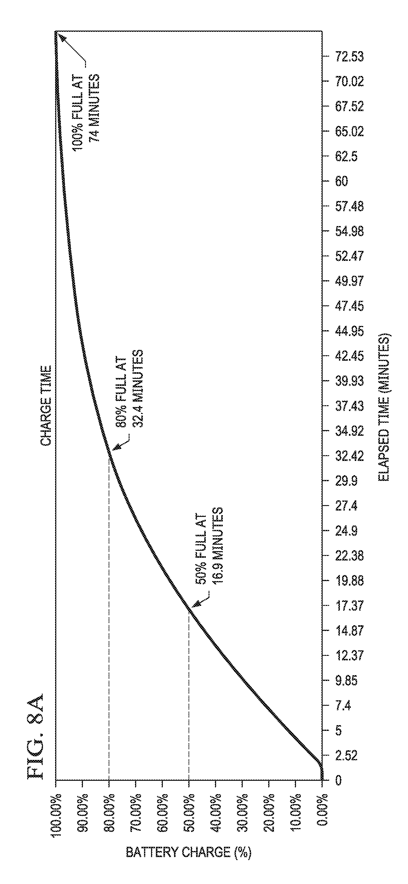
[0039] FIGS. 8A and 8B provide example plots illustrating example charge-cycle data and example total charge-time data.
[0040] FIGS. 9A and 9B illustrates an example switched-capacitor current multiplication battery charger 20 according to the Disclosure, configured with a dual power stage (power phase).
[0041] The switched-capacitor current multiplication battery charger 20 receives power from the adapter 5 (through transistor M1). The battery charger includes dual-stage switches Q1-Q4 and Q5-Q8, controlled to alternately charge and discharge respective flying (charge pump) capacitors CFLY1 and CFLY2. FIG. 1B illustrates example waveforms for V(BUS), V(BAT), I(BUS), I(BAT), and I(CFLY).
[0042] As described above in connection with the single stage/phase switched-capacitor current multiplication battery charger, the CFLY1 and CFLY2 capacitors can be implemented with two to four CFLY capacitors per phase.
[0043] FIGS. 10A and 10B provide example plots illustrating improvements in efficiency and ripple performance for multi-phase configurations.
[0044] FIGS. 11A and 11B illustrate an example battery charge system board implementation, such as for a mobile phone, including a dual-phase switched-capacitor current multiplication battery charger 30 according to the Disclosure. FIG. 11B illustrates example system load response with V(BUS), V(BAT), I(BUS), I(BAT), and ICFLY1/ICFLY2.
[0045] Switched-capacitor current multiplication is implemented as an example current doubler. The switched-capacitor current multiplication battery charger 30 includes dual-phase CFLY terminals CTOP1/CBOT1 and CTOP2/CBOT2.
[0046] The switched-capacitor current multiplication battery charger architecture according to the Disclosure enable high current batter charging, while reducing the current across the bus/cable, reducing I.sup.2R losses in R.sub.CONA, R.sub.CABLE, R.sub.COND and R.sub.CONTROL. Converter efficiency (n) can be increased to reduce power loss and thermals. Protections ensure that the battery charger can monitor all key system aspects for overvoltage, overcurrent and temperature. All USB Type-C.TM. cables can support between 3 A at 20 V, 5 A at 20 V.
[0047] The switched-capacitor topology enables the delivery of high current to the battery while keeping bus/cable current and voltage drops low. For example, the battery charging architecture can enable 6-A battery charging with standard 3-A-capable USB Type-C cables, delivering up to 10 A with 5-A-capable cables when using switched-capacitor devices in parallel. The switched-capacitor architecture can achieve up to 97% efficiency at 6 A delivered to the battery with only 3 A required on the USB Type-C cable, which means less than 800 mW of dissipation in the device, while requiring less than 3 A on a standard USB Type-C cable.
[0048] The switched-capacitor architecture can be used with a smart adapter to regulate the voltage and current at the input to the charger. The USB PD PPS protocol allows a sink directed source output. In this case the sink is the device and the source is the adapter. When the wall adapter is not in current foldback, the device directs the voltage output in 20-mV steps, acting as a current-limited voltage source. When the adapter is in current foldback, the adapter can maintain the voltage, and the device can direct the output current in 50-mA steps.
[0049] In summary, a system for charging a battery includes an adapter, and a charger coupled to receive power from the adapter, and to provide a charging current to the battery. The charger includes a power stage with a charge pump to provide the charging current, and a feedback circuit to provide a feedback signal to the adapter. The power stage can be one of: an adjustable current source with voltage clamp, and an adjustable voltage source with current clamp. The charge pump can be implemented as a voltage divider, so that an input adapter current is multiplied by a pre-defined divider ratio to provide the charging current. The charge pump can be one of: single-phase; and multi-phase.
[0050] The system does not require inductors, or can be implemented with small value inductors. Battery charging parameters (current, voltage etc.) are controlled by feedback regulating the adapter output current or voltage. Feedback from the charger to the adapter can be analog or digital, continuous time or sampled.
[0051] Charging is controlled as an entire system (adapter and charger working as single system). Can be adapted for use with rapid-charge adapter technology (such as FlashCharge). Uses efficient (>97%), and simple (no internal regulation) charge-pump energy conversion. No inductor is required
[0052] Advantages include: (a) Very high efficiency (for example, 97% @6 A); (b) small solution size (no inductor); and (c) interfaces with new rapid-charge adapter technology by multiplying the available charging current.
[0053] The Disclosure provided by this Description and the Figures sets forth example designs and applications illustrating aspects and features of the invention, and does not limit the scope of the invention, which is defined by the claims. Known circuits, connections, functions and operations are not described in detail to avoid obscuring the principles and features of the Disclosed example designs and applications. This Disclosure can be used by ordinarily skilled artisans as a basis for modifications, substitutions and alternatives, including adaptations for other applications.
* * * * *
D00000
D00001
D00002
D00003
D00004
D00005
D00006
D00007
D00008
D00009
D00010
D00011
D00012

D00013

D00014

D00015

D00016

XML
uspto.report is an independent third-party trademark research tool that is not affiliated, endorsed, or sponsored by the United States Patent and Trademark Office (USPTO) or any other governmental organization. The information provided by uspto.report is based on publicly available data at the time of writing and is intended for informational purposes only.
While we strive to provide accurate and up-to-date information, we do not guarantee the accuracy, completeness, reliability, or suitability of the information displayed on this site. The use of this site is at your own risk. Any reliance you place on such information is therefore strictly at your own risk.
All official trademark data, including owner information, should be verified by visiting the official USPTO website at www.uspto.gov. This site is not intended to replace professional legal advice and should not be used as a substitute for consulting with a legal professional who is knowledgeable about trademark law.