Semiconductor Structure And Manufacturing Method Of The Same
Li; Shin-Hung ; et al.
U.S. patent application number 16/102847 was filed with the patent office on 2019-04-18 for semiconductor structure and manufacturing method of the same. The applicant listed for this patent is UNITED MICROELECTRONICS CORP.. Invention is credited to Kuan-Chuan Chen, Wen-Fang Lee, Nien-Chung Li, Shin-Hung Li, Chih-Chung Wang.
| Application Number | 20190115469 16/102847 |
| Document ID | / |
| Family ID | 63556818 |
| Filed Date | 2019-04-18 |


| United States Patent Application | 20190115469 |
| Kind Code | A1 |
| Li; Shin-Hung ; et al. | April 18, 2019 |
SEMICONDUCTOR STRUCTURE AND MANUFACTURING METHOD OF THE SAME
Abstract
A semiconductor structure and a manufacturing method of a semiconductor structure are provided. The semiconductor structure includes a semiconductor substrate, a gate, a first diffusion region and a second diffusion region. The gate is disposed on the semiconductor substrate and extends along a first direction. The first diffusion region is formed in the semiconductor substrate, and the second diffusion region is formed in the first diffusion region. The first diffusion region has a first portion located underneath the gate and a second portion protruded from a lateral side of the gate, the first portion has a first length parallel to the first direction, the second portion has a second length parallel to the first direction, and the first length is larger than the second length.
| Inventors: | Li; Shin-Hung; (Caotun Township, TW) ; Chen; Kuan-Chuan; (Taichung City, TW) ; Li; Nien-Chung; (Hsinchu City, TW) ; Lee; Wen-Fang; (Hsinchu City, TW) ; Wang; Chih-Chung; (Hsinchu City, TW) | ||||||||||
| Applicant: |
|
||||||||||
|---|---|---|---|---|---|---|---|---|---|---|---|
| Family ID: | 63556818 | ||||||||||
| Appl. No.: | 16/102847 | ||||||||||
| Filed: | August 14, 2018 |
Related U.S. Patent Documents
| Application Number | Filing Date | Patent Number | ||
|---|---|---|---|---|
| 15785606 | Oct 17, 2017 | 10084083 | ||
| 16102847 | ||||
| Current U.S. Class: | 1/1 |
| Current CPC Class: | H01L 29/0649 20130101; H01L 29/66575 20130101; H01L 21/823481 20130101; H01L 29/42372 20130101; H01L 21/3086 20130101; H01L 29/7836 20130101; H01L 21/76224 20130101; H01L 29/36 20130101; H01L 29/0692 20130101; H01L 29/0847 20130101; H01L 21/26513 20130101; H01L 21/324 20130101; G03F 1/36 20130101; H01L 27/088 20130101; H01L 27/0207 20130101; H01L 29/7833 20130101; H01L 21/823418 20130101 |
| International Class: | H01L 29/78 20060101 H01L029/78; H01L 29/66 20060101 H01L029/66; H01L 27/088 20060101 H01L027/088; H01L 21/324 20060101 H01L021/324; H01L 21/762 20060101 H01L021/762; H01L 21/265 20060101 H01L021/265; H01L 21/308 20060101 H01L021/308; H01L 27/02 20060101 H01L027/02; H01L 29/06 20060101 H01L029/06; H01L 29/36 20060101 H01L029/36; H01L 29/08 20060101 H01L029/08; H01L 29/423 20060101 H01L029/423; G03F 1/36 20060101 G03F001/36 |
Claims
1. A manufacturing method of a semiconductor structure, comprising: providing a semiconductor substrate; providing a photomask having a layout pattern; forming a first diffusion region in the semiconductor substrate according to the layout pattern, wherein the first diffusion region has a first portion and a second portion connected to each other, the first portion has a first length parallel to a first direction, the second portion has a second length parallel to the first direction, and the first length is larger than the second length; forming a gate on the semiconductor substrate, wherein the gate extends along the first direction, the first portion of the first diffusion region is located underneath the gate, and the second portion of the first diffusion region is protruded from a lateral side of the gate; and forming a second diffusion region in the first diffusion region.
2. The manufacturing method of the semiconductor structure according to claim 1, wherein the first length is larger than the second length by at least 15 nm.
3. The manufacturing method of the semiconductor structure according to claim 1, wherein the first portion and the second portion of the first diffusion region form a T-shaped pattern.
4. The manufacturing method of the semiconductor structure according to claim 1, wherein forming the gate on the semiconductor substrate is after forming the first diffusion region in the semiconductor substrate.
5. The manufacturing method of the semiconductor structure according to claim 1, wherein the second diffusion region has a higher dopant concentration than the first diffusion region.
6. The manufacturing method of the semiconductor structure according to claim 1, further comprising: forming a mask layer on the semiconductor substrate; transferring the layout pattern from the photomask to the mask layer; and forming a plurality of trenches in the semiconductor substrate by etching the semiconductor substrate according to the mask layer having the transferred layout pattern; and filling an insulating material in the trenches to form a shallow trench isolation in the semiconductor structure.
7. The manufacturing method of the semiconductor structure according to claim 6, wherein forming the first diffusion region in the semiconductor substrate further comprising: performing an implantation process on a region of the semiconductor substrate enclosed by the shallow trench isolation; and performing a thermal process on the region.
8. The manufacturing method of the semiconductor structure according to claim 1, wherein the layout pattern has a first pattern and a second pattern connected to each other, the first pattern has a first pattern length parallel to the first direction, the second pattern has a second pattern length parallel to the first direction, and the first pattern length is larger than the second pattern length.
9. The manufacturing method of the semiconductor structure according to claim 8, wherein the first pattern and the second pattern of the layout pattern form a T-shaped pattern.
10. The manufacturing method of the semiconductor structure according to claim 1, further comprising: performing an optical proximity correction process for the layout pattern.
Description
[0001] This application is a divisional application of U.S. application Ser. No. 15/785,606, filed on Oct. 17, 2017. The entire content of the related application is incorporated herein by reference.
BACKGROUND
Technical Field
[0002] The present disclosure relates in general to a semiconductor structure and a manufacturing method thereof, and more particularly to a semiconductor structure with double diffused drains (DDD) and a manufacturing method thereof.
Description of the Related Art
[0003] With the developments of semiconductor technology, in addition to high voltage devices, medium voltage devices are widely applied to a variety of electronic products in different fields as well. For example, applications of medium voltage devices include I/O, DAC, OPT, MTP, and etc., and the occupied area of medium voltage devices in the overall device may be up to 20% to 50%. While a double diffused drain (DDD) usually provides a higher breakdown voltage, a DDDMOS device may be included in the applications of medium voltage devices as well. Therefore, researches and developments in the designs of applying such devices in the applications of medium voltage devices have been disclosed.
SUMMARY OF THE INVENTION
[0004] The present disclosure is directed to a semiconductor structure and a manufacturing method thereof. According to the embodiments of the present disclosure, the first length of the first portion of the first diffusion region located under the gate is larger than the second length of the second portion of the first diffusion region protruded from a lateral side of the gate, such that the design rule of the first diffusion region under the channel region can be maintained for the desired electrical performance (i.e. Vt stability, desired on-resistance, and etc.), and the total area of the first diffusion region can be reduced for further reducing the device size.
[0005] According to an embodiment of the present disclosure, a semiconductor structure is disclosed. The semiconductor structure includes a semiconductor substrate, a gate, a first diffusion region and a second diffusion region. The gate is disposed on the semiconductor substrate and extends along a first direction. The first diffusion region is formed in the semiconductor substrate, and the second diffusion region is formed in the first diffusion region. The first diffusion region has a first portion located underneath the gate and a second portion protruded from a lateral side of the gate, the first portion has a first length parallel to the first direction, the second portion has a second length parallel to the first direction, and the first length is larger than the second length.
[0006] According to another embodiment of the present disclosure, a manufacturing method of a semiconductor structure is disclosed. The manufacturing method of the semiconductor structure includes the following steps: providing a semiconductor substrate; providing a photomask having a layout pattern; forming a first diffusion region in the semiconductor substrate according to the layout pattern, wherein the first diffusion region has a first portion and a second portion connected to each other, the first portion has a first length parallel to a first direction, the second portion has a second length parallel to the first direction, and the first length is larger than the second length; forming a gate on the semiconductor substrate, wherein the gate extends along the first direction, the first portion of the first diffusion region is located underneath the gate, and the second portion of the first diffusion region is protruded from a lateral side of the gate; and forming a second diffusion region in the first diffusion region.
[0007] The disclosure will become apparent from the following detailed description of the preferred but non-limiting embodiments. The following description is made with reference to the accompanying drawings.
BRIEF DESCRIPTION OF THE DRAWINGS
[0008] FIG. 1A shows a top view of a semiconductor structure according to an embodiment of the present disclosure;
[0009] FIG. 1B shows a cross-sectional view along the cross-sectional line 1B-1B' in FIG. 1A;
[0010] FIG. 10 shows a cross-sectional view along the cross-sectional line 1C-1C' in FIG. 1A;
[0011] FIG. 2A shows a top view of a semiconductor structure according to another embodiment of the present disclosure;
[0012] FIG. 2B shows a cross-sectional view along the cross-sectional line 2B-2B' in FIG. 2A; and
[0013] FIG. 3A to FIG. 9 show a manufacturing method of a semiconductor structure according to an embodiment of the present disclosure.
DETAILED DESCRIPTION OF THE INVENTION
[0014] According to the embodiments of the present disclosure, a semiconductor structure and a manufacturing method thereof are provided. The embodiments are described in details with reference to the accompanying drawings. The details of the embodiments are for exemplification only, not for limiting the scope of protection of the disclosure. Moreover, the identical or similar elements of the embodiments are designated with the same reference numerals. Also, it is also important to point out that the illustrations may not be necessarily be drawn to scale, and that there may be other embodiments of the present disclosure which are not specifically illustrated. Thus, the specification and the drawings are to be regarded as an illustrative sense rather than a restrictive sense. It is to be noted that the drawings are simplified for clearly describing the embodiments, and the details of the structures and the manufacturing processing steps of the embodiments are for exemplification only, not for limiting the scope of protection of the disclosure. Ones having ordinary skills in the art may modify or change the structures and the manufacturing processing steps according to the embodiments of the present disclosure.
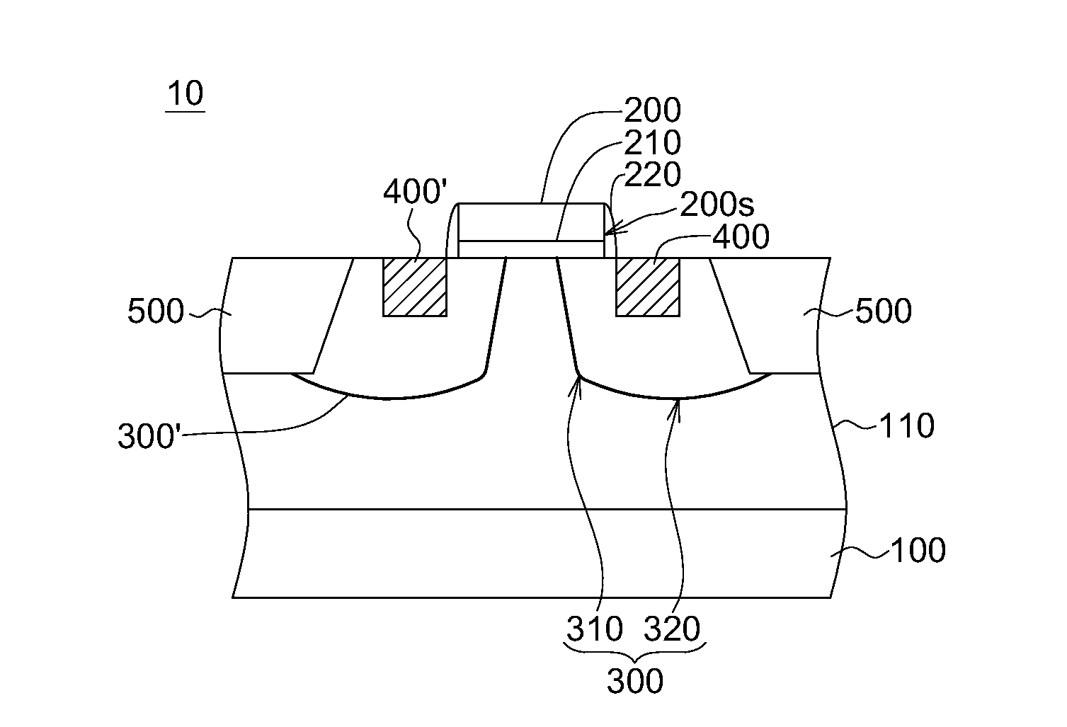
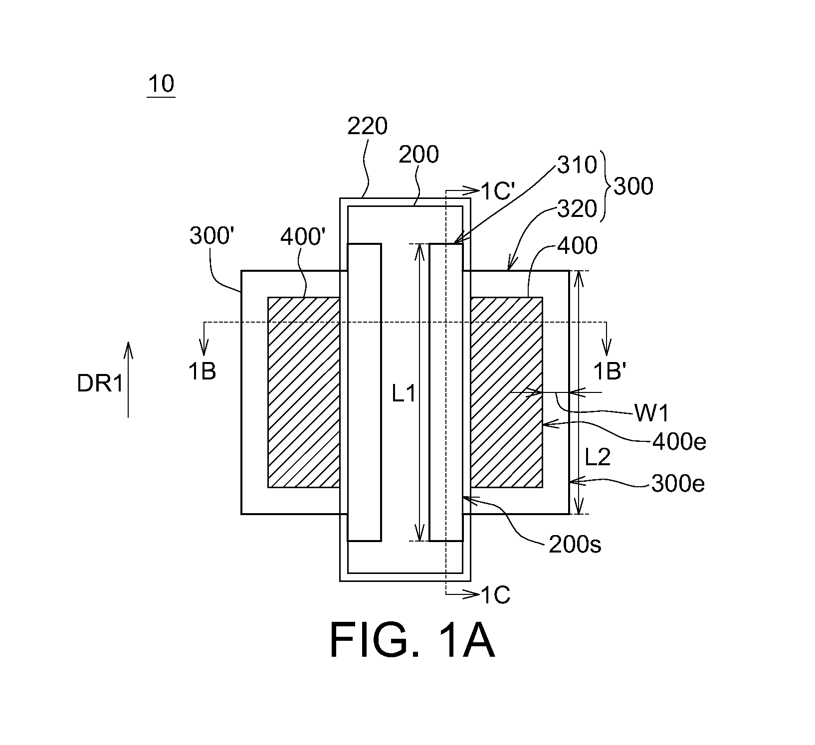
[0015] FIG. 1A shows a top view of a semiconductor structure according to an embodiment of the present disclosure, FIG. 1B shows a cross-sectional view along the cross-sectional line 1B-1B' in FIG. 1A, and FIG. 10 shows a cross-sectional view along the cross-sectional line 1C-1C' in FIG. 1A.
[0016] As shown in FIGS. 1A-1C, the semiconductor structure 10 includes a semiconductor substrate 100, a gate 200, a first diffusion region 300 and a second diffusion region 400. The gate 200 is disposed on the semiconductor substrate 100 and extends along a first direction DR1. The first diffusion region 300 is formed in the semiconductor substrate 100, and the second diffusion region 400 is formed in the first diffusion region 300. The first diffusion region 300 has a first portion 310 located underneath the gate 200 and a second portion 320 protruded from a lateral side 200s of the gate 200, the first portion 310 has a first length L1 parallel to the first direction DR1, the second portion 320 has a second length L2 parallel to the first direction DR1, and the first length L1 is larger than the second length L2.
[0017] As shown in FIG. 1A, in the embodiments, the first length L1 is larger than the second length L2 by at least 15 nm.
[0018] As shown in FIG. 1A, the first portion 310 and the second portion 320 of the first diffusion region 300 form a T-shaped pattern.
[0019] In the embodiments, as shown in FIG. 1A and FIG. 1B, the second diffusion region 400 is formed in the second portion 320 of the first diffusion region 300, and the second diffusion region 400 has a higher dopant concentration than the first diffusion region 300.
[0020] As shown in FIGS. 1B and 1C, the semiconductor structure 10 may further include a shallow trench isolation (STI) 500, and the shallow trench isolation 500 is formed in the semiconductor substrate 100 defining the first diffusion region 300. That is, in the structure as shown in FIGS. 1A-1C, the shallow trench isolation 500 (not shown in FIG. 1A) abuts the outer edges of the first portion 310 and the second portion 320 of the first diffusion region 300.
[0021] In the embodiments, as shown in FIG. 1A, the outer edge 300e of the first diffusion region 300 is separated from the outer edge 400e of the second diffusion region 400 by a distance W1. When the T-shaped pattern of the first diffusion region 300 including the first portion 310 having the first length L1 and the second portion 320 having the second length L2 is designed, the first length L1 is determined according to the desired electrical performance to be achieved, and then the second length L2 is determined by subtracting the first length L1 by the distance W1. As such, the distance W1 may be regarded as the reduced extent of the second portion 320 of the first diffusion region 300.
[0022] In some embodiments, the distance W1 may be 9 nm to 17 nm; in other embodiments, the distance W1 may vary according to actual needs and is not limited thereto.
[0023] In some embodiments, as shown in FIG. 1A and FIG. 1B, the semiconductor structure 10 further include another first diffusion region 300' and another second diffusion region 400' formed in the semiconductor substrate 100, the second diffusion region 400' is formed in the first diffusion region 300', the first diffusion regions 300 and 300' are located on two opposite sides of the gate 200, and the second diffusion regions 400 and 400' are located on two opposite sides of the gate 200. As shown in FIG. 1A and FIG. 1B, the first diffusion region 300' may have the same T-shaped pattern as that of the first diffusion region 300.
[0024] As shown in FIG. 1B and FIG. 1C, the semiconductor structure 10 may further include an oxide layer 210 and a spacer 220, the oxide layer 210 is formed between the semiconductor substrate 100 and the gate 200, and the spacer 220 is formed on the sidewall of the gate 200.
[0025] As shown in FIG. 1B and FIG. 1C, the semiconductor structure 10 may further include a lightly-doped region 110 formed in the semiconductor substrate 100, and the lightly-doped region 110 encompasses the first diffusion regions 300 and 300' and the second diffusion regions 400 and 400'.
[0026] In the embodiments, the second diffusion regions 400 and 400' are such as drain/source regions, the first diffusion regions 300 and 300' surround the drain/source regions, and the semiconductor structure 10 is such as a double diffused drains (DDD) MOS device.
[0027] In DDDMOS devices, for example, medium voltage (MV) DDDMOS devices, the design rule of the diffusion region under the gate (e.g. channel region) is important to the electrical performance of the MV DDDMOS device, such as stability of threshold voltage (Vt), the prevention of undesired junction breakdown and the desired value of on-resistance. According to the embodiments of the present disclosure, the first length L1 of the first portion 310 of the first diffusion region 300 is larger than the second length L2 of the second portion 320 of the first diffusion region 300, such that the design rule of the first diffusion region 300 under the channel region can be maintained for the desired electrical performance (i.e. Vt stability, desired on-resistance, and etc.), and the total area of the first diffusion region 300 can be reduced for further reducing the device size.
[0028] Table 1 below shows breakdown voltages of semiconductor structures with the second portions 320 of the first diffusion regions 300 having different occupied areas according to some embodiments of the present disclosure. While the area of the second diffusion region 400 remains constant, the different occupied areas of the second portions 320 are represented by the different values of the distance W1.
TABLE-US-00001 TABLE 1 Embodi- Embodi- Embodi- Embodi- Embodi- ment 1-1 ment 1-2 ment 1-3 ment 1-4 ment 1-5 Distance 17 15 13 11 9 W1 (nm) Breakdown 13.6 13.5 13.3 12.9 12.6 voltage (V)
[0029] As shown in table 1, as the width W1 varies from 17 nm to 9 nm, indicating the occupied area of the second portion 320 being greatly reduced, the breakdown voltage is only slightly decreased from 13.6V to 12.6V. As such, with the design of the first portion 310 and the second portion 320 of the first diffusion region 300 according to the embodiments of the present disclosure, the desired electrical performance (i.e. Vt stability, desired on-resistance, and etc.) can be maintained, and the breakdown voltages is only slightly influenced yet still remained in the range of the operation voltage of medium voltage devices.
[0030] FIG. 2A shows a top view of a semiconductor structure according to another embodiment of the present disclosure, and FIG. 2B shows a cross-sectional view along the cross-sectional line 2B-2B' in FIG. 2A. The elements in the present embodiment sharing similar or the same labels with those in the previous embodiment are similar or the same elements, and the description of which is omitted.
[0031] As shown in FIG. 2A and FIG. 2B, the semiconductor structure 20 may further include an additional gate 600, an additional first diffusion region 700 and an additional second diffusion region 800. The additional gate 600 is disposed on the semiconductor substrate 100 and extends along a second direction DR2 which is perpendicular to the first direction DR1. The additional first diffusion region 700 is formed in the semiconductor substrate 100. The additional second diffusion region 800 is formed in the additional first diffusion region 700 and separated from the first diffusion region 300 by a predetermined minimum distance D1.
[0032] As shown in FIG. 2A and FIG. 2B, the semiconductor structure 20 includes two MOS devices arranged vertically to each other; that is, the extending direction of the gate 200 and the extending direction of the additional gate 600 are perpendicular to each other. In the embodiments, as shown in FIG. 2B, the shallow trench isolation 500 is formed in the semiconductor substrate 100 defining the first diffusion region 300, and the shallow trench isolation 500 may define the additional first diffusion region 700 as well. That is, in the structure as shown in FIGS. 2A-2B, the shallow trench isolation 500 (not shown in FIG. 2A) abuts the outer edges of the first portion 310 and the second portion 320 of the first diffusion region 300, and the shallow trench isolation 500 may also abut the outer edges of the additional first diffusion region 700. As shown in FIG. 2A and FIG. 2B, while the diffusion regions are all formed before the formation of the gate 200 and the additional gate 600, the predetermined minimum distance D1 provides the variation tolerance for the implantation processes of the diffusion regions, such that the first diffusion region 300 of one MOS device does not overlap the channel region 630 of another MOS device, and thus short circuit can be effectively prevented.
[0033] In some embodiments, the predetermined minimum distance D1 may be at least 50 nm; in other embodiments, the predetermined minimum distance D1 may be less than 50 nm or larger than 50 nm. The predetermined minimum distance D1 is determined basically according to the limitations and variation tolerance of the manufacturing processes and thus may vary according to actual situations.
[0034] As shown in FIG. 2A, as the pitch size of the semiconductor structure 20 including multiple MOS devices are determined by the distance between adjacent MOS devices, which is determined from the predetermined minimum distance D1, the distance W1 and the second length L2, it is clear that with the design of the first diffusion region 300 according to the embodiments of the present disclosure, the pitch size of the semiconductor structure 20 can be effectively reduced.
[0035] Table 2 below shows size parameters of semiconductor structures according to some embodiments and a comparative embodiment of the present disclosure. In table 2, "Voltage" refers to the operation voltage, "D2D rule" refers to the distance between the second diffusion region 400 and the additional second diffusion region 800 (i.e. the distance between drains of adjacent MOS devices), "L pitch" refers to the distance between the second diffusion region 400 and another second diffusion region of another MOS device (not shown in drawings) along the first direction DR1, "W pitch" refers to the distance between the second diffusion region 400 and the additional second diffusion region 800, and "Area" refers to the area calculated by "L pitch" multiplied by "W pitch". In the structure of comparative embodiment 1, the diffusion regions for the drains do not have the structural design of the first diffusion region 300 according to the embodiments of the present disclosure.
TABLE-US-00002 TABLE 2 Voltage D2D rule L pitch W pitch Area Reduced (V) (.mu.m) (.mu.m) (.mu.m) (.mu.m.sup.2) area (%) Comparative 8 0.230 1.429 0.480 0.686 0 embodiment 1 Embodiment 8 0.212 1.411 0.462 0.653 5.2 2-1 Embodiment 6 0.212 1.177 0.462 0.544 5.4 2-2 Embodiment 3.3 0.212 1.078 0.462 0.498 5.6 2-3
[0036] As shown in table 2, the structure of the embodiment 2-1 has a first diffusion region 300 with the first length L1 larger than the second length L2 by 18 nm, and while the operation voltages for comparative embodiment 1 and embodiment 2-1 are the same, the pitch area of the structure of embodiment 2-1 is reduced by 5.2%. Similarly, with the design of the first diffusion region 300 according to the embodiments of the present disclosure, the devices can function well under medium operation voltages with reduced device sizes.
[0037] As shown in FIGS. 2A and 2B, the semiconductor structure 20 may further include an oxide layer 610 and a spacer 620, the oxide layer 610 is formed between the semiconductor substrate 100 and the additional gate 600, and the spacer 620 is formed on the sidewall of the additional gate 600.
[0038] In some embodiments, as shown in FIG. 2A and FIG. 2B, a portion of the additional gate 600 may be located on the first diffusion region 300.
[0039] In the embodiments, as shown in FIG. 2A and FIG. 2B, the first diffusion region 300 and the additional first diffusion region 700 are separated from each other by a distance D2. In some other embodiments, the first diffusion region 300 and the additional first diffusion region 700 may be overlapped (not shown in drawings).
[0040] In the embodiments, the additional first diffusion region 700 may have a T-shaped pattern similar to that of the first diffusion region 300. For example, as shown in FIG. 2A, the additional first diffusion region 700 may have a third portion 710 and a fourth portion 720, the third portion 710 is located underneath the additional gate 600, the fourth portion 720 is protruded from a lateral side 600s of the additional gate 600, the third portion 710 has a third length L3 parallel to the second direction DR2, the fourth portion 720 has a fourth length L4 parallel to the second direction DR2, and the third length L3 is larger than the fourth length L4.
[0041] As shown in FIG. 2A and FIG. 2B, the semiconductor structure 20 further include another additional first diffusion region 700' and another additional second diffusion region 800' formed in the semiconductor substrate 100, the additional second diffusion region 800' is formed in the additional first diffusion region 700', the additional first diffusion regions 700 and 700' are located on two opposite sides of the additional gate 600, and the additional second diffusion regions 800 and 800' are located on two opposite sides of the additional gate 600. As shown in FIG. 2A and FIG. 2B, the additional first diffusion region 700' may have the same T-shaped pattern as that of the additional first diffusion region 700.
[0042] FIG. 3A to FIG. 9 show a manufacturing method of a semiconductor structure according to an embodiment of the present disclosure. The elements in the present embodiment sharing similar or the same labels with those in the previous embodiments are similar or the same elements, and the description of which is omitted.
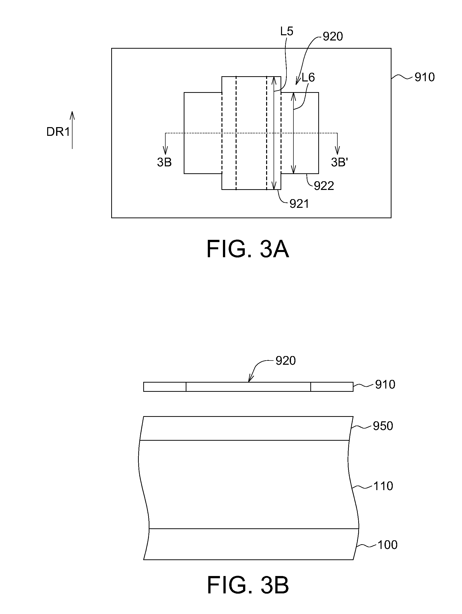
[0043] Referring to FIG. 3A and FIG. 3B (FIG. 3A shows a top view of the present step, and FIG. 3B shows a cross-sectional view along the cross-sectional line 3B-3B' in FIG. 3A), a semiconductor substrate 100 is provided, and a photomask 910 having a layout pattern 920 is provided.
[0044] As shown in FIG. 3A, the layout pattern 920 has a first pattern 921 and a second pattern 922 connected to each other, the first pattern 921 has a first pattern length L5 parallel to the first direction DR1, the second pattern 922 has a second pattern length L6 parallel to the first direction DR1, and the first pattern length L5 is larger than the second pattern length L6. As shown in FIG. 3A, the first pattern 921 and the second pattern 922 of the layout pattern 920 form a T-shaped pattern.
[0045] In the embodiments, an optical proximity correction process may be further performed for the layout pattern 920.
[0046] As shown in FIG. 3B, a lightly-doped region 110 is formed in the semiconductor substrate 100, and a mask layer 950 is formed on the semiconductor substrate 100.
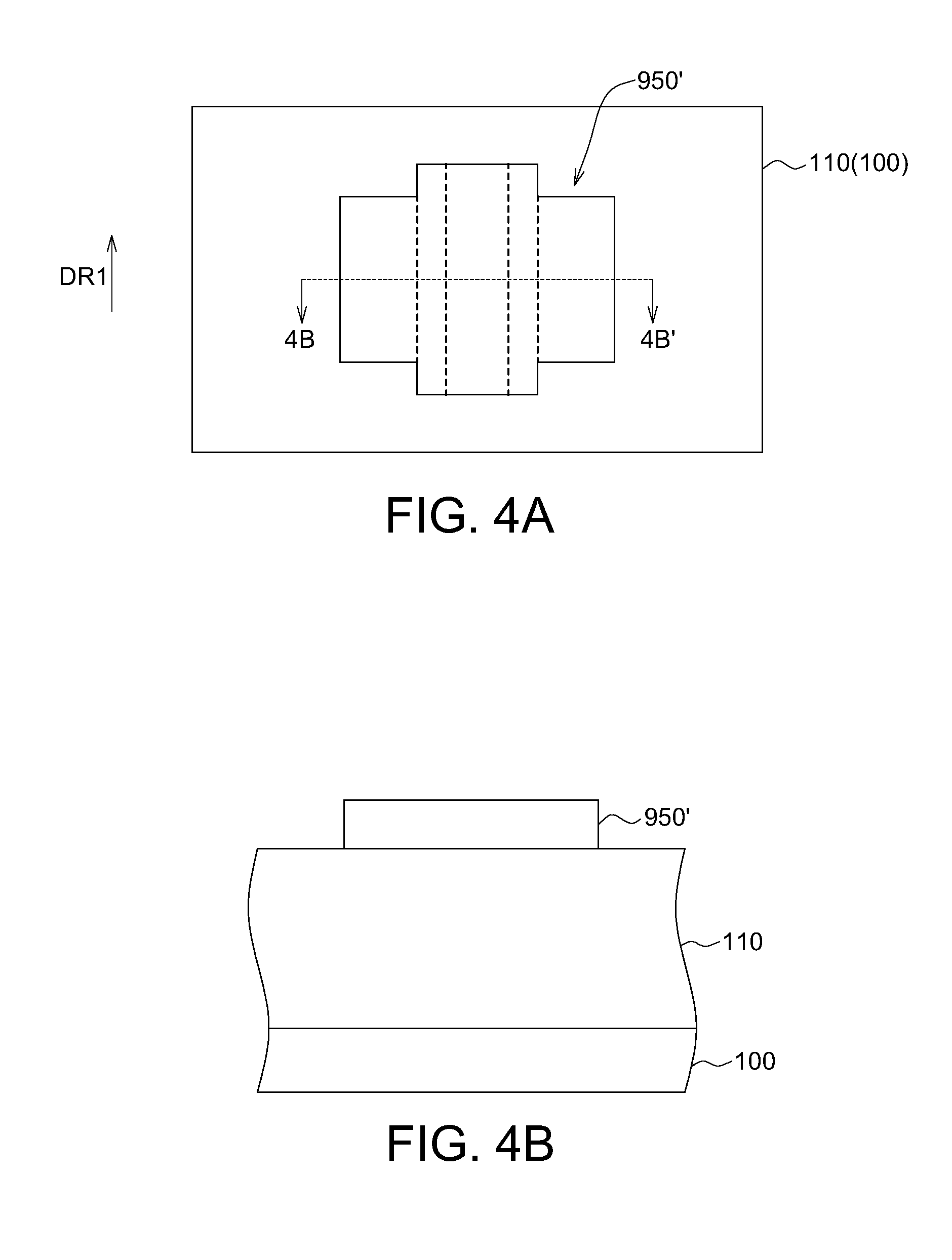
[0047] Referring to FIG. 4A and FIG. 4B (FIG. 4A shows a top view of the present step, and FIG. 4B shows a cross-sectional view along the cross-sectional line 4B-4B' in FIG. 4A), the layout pattern 920 is transferred from the photomask 910 to the mask layer 950 to form a patterned mask layer 950' having the transferred layout pattern.
[0048] Next, referring to FIG. 5A and FIG. 5B (FIG. 5A shows a top view of the present step, and FIG. 5B shows a cross-sectional view along the cross-sectional line 5B-5B' in FIG. 5A), a plurality of trenches T are formed in the semiconductor substrate 100 by etching the semiconductor substrate 100 according to the patterned mask layer 950' having the transferred layout pattern.
[0049] Next, referring to FIG. 6, an insulating material is filled in the trenches T to form a shallow trench isolation 500 in the semiconductor structure 100.
[0050] Next, referring to FIG. 7 to FIG. 8, a first diffusion region 300 is formed in the semiconductor substrate 100 according to the layout pattern 920. The process for forming the first diffusion region 300 may include the following steps.
[0051] As shown in FIG. 7, an implantation process IMP is performed on a region R of the semiconductor substrate 100 enclosed by the shallow trench isolation 500. It is to be noted that in the present implantation process, the region R with dopants is smaller than the first diffusion region 300 to-be-formed, and the formation of the first diffusion region 300 will be completed after at least a thermal process is performed on the region R subsequently, as described hereinafter.
[0052] Next, as shown in FIG. 8, after at least a thermal process is performed on the region R, the dopants in the region R is driven by the thermal process to diffuse, the doped region is thus enlarged, and then the region R with dopants is expanded until stopped by the shallow trench isolation 500, thereby the first diffusion region 300 is formed.
[0053] As shown in FIG. 8, an oxide layer 210 is formed on the semiconductor substrate 100. In the embodiments, the process of forming the oxide layer 210 requires heating, and the aforementioned thermal process for forming the first diffusion region 300 may be realized by the process of forming the oxide layer 210. That is, as the oxide layer 210 is formed on the semiconductor substrate 100 at an elevated temperature, this thermal process facilitates the expansion of the region R with dopants for forming the first diffusion region 300. In the embodiments, in addition to the process of forming the oxide layer 210, there may be other processes requiring heating performed before the step of forming the gate 200 on the semiconductor substrate 100, and these thermal processes may be included in the aforementioned thermal process for forming the first diffusion region 300.
[0054] As shown in FIG. 8, after the first diffusion region 300 is formed in the semiconductor substrate 100, the gate 200 is formed on the semiconductor substrate 100.
[0055] Next, referring to FIGS. 1A-1C and FIG. 9, the second diffusion region 400 is formed in the first diffusion region 300 by such as an implantation process. As shown in FIGS. 1A-1C and FIG. 9, in the as-formed semiconductor structure 10, the first diffusion region 300 has a first portion 310 located underneath the gate 200 and a second portion 320 protruded from a lateral side 200s of the gate 200, the first portion 310 has a first length L1 parallel to the first direction DR1, the second portion 320 has a second length L2 parallel to the first direction DR1, and the first length L1 is larger than the second length L2.
[0056] Table 3 below shows some processing deviations in selected steps in the manufacturing process according to some embodiments of the present disclosure, and the aforementioned predetermined minimum distance D1 may be determined according to these parameters. In table 3, "CD bar" refers to the critical dimension bar in the step of transferring a layout pattern from a photomask to a mask layer, "AA" refers to the processing deviation in the step of forming trenches according to the mask with the transferred layout pattern, and "Spec limited" refers to the minimum deviation tolerance of the predetermined minimum distance D1 determined according to "CD bar" and "AA". The units are all in "nm". In embodiment 3-1, the first diffusion region 300 is N-type doped, and in embodiment 3-2, the first diffusion region 300 is P-type doped.
TABLE-US-00003 TABLE 3 CD bar CD 3.sigma. AA AA 3.sigma. Spec limited Embodiment 3-1 162 .+-. 16 7.6 .+-.25 17 41 Embodiment 3-2 162 .+-. 16 11.1 .+-.25 15 41
[0057] According to the results as shown in table 3, the predetermined minimum distance D1 is determined to be larger than the value as shown in "Spec limited"; that is, when designing the layout pattern, in the present embodiments for example, a predetermined minimum distance D1 of at least larger than 41 nm should be included in the consideration and design of the shape and size of the layout pattern. It is to be noted that table 3 shows an example of how the predetermined minimum distance D1 may be determined; however, the present disclosure is not limited thereto.
[0058] While the disclosure has been described by way of example and in terms of the preferred embodiment(s), it is to be understood that the disclosure is not limited thereto. On the contrary, it is intended to cover various modifications and similar arrangements and procedures, and the scope of the appended claims therefore should be accorded the broadest interpretation so as to encompass all such modifications and similar arrangements and procedures.
* * * * *
D00000
D00001
D00002
D00003
D00004
D00005
D00006
D00007
D00008
XML
uspto.report is an independent third-party trademark research tool that is not affiliated, endorsed, or sponsored by the United States Patent and Trademark Office (USPTO) or any other governmental organization. The information provided by uspto.report is based on publicly available data at the time of writing and is intended for informational purposes only.
While we strive to provide accurate and up-to-date information, we do not guarantee the accuracy, completeness, reliability, or suitability of the information displayed on this site. The use of this site is at your own risk. Any reliance you place on such information is therefore strictly at your own risk.
All official trademark data, including owner information, should be verified by visiting the official USPTO website at www.uspto.gov. This site is not intended to replace professional legal advice and should not be used as a substitute for consulting with a legal professional who is knowledgeable about trademark law.