Methods Of Forming A Semiconductor Device Using Block Copolymer Materials
Millward; Dan B. ; et al.
U.S. patent application number 16/215242 was filed with the patent office on 2019-04-18 for methods of forming a semiconductor device using block copolymer materials. The applicant listed for this patent is Micron Technology, Inc.. Invention is credited to Dan B. Millward, Timothy A. Quick.
| Application Number | 20190115252 16/215242 |
| Document ID | / |
| Family ID | 40612928 |
| Filed Date | 2019-04-18 |


View All Diagrams
| United States Patent Application | 20190115252 |
| Kind Code | A1 |
| Millward; Dan B. ; et al. | April 18, 2019 |
METHODS OF FORMING A SEMICONDUCTOR DEVICE USING BLOCK COPOLYMER MATERIALS
Abstract
Methods for fabricating sub-lithographic, nanoscale microstructures utilizing self-assembling block copolymers, and films and devices formed from these methods are provided.
| Inventors: | Millward; Dan B.; (Boise, ID) ; Quick; Timothy A.; (Boise, ID) | ||||||||||
| Applicant: |
|
||||||||||
|---|---|---|---|---|---|---|---|---|---|---|---|
| Family ID: | 40612928 | ||||||||||
| Appl. No.: | 16/215242 | ||||||||||
| Filed: | December 10, 2018 |
Related U.S. Patent Documents
| Application Number | Filing Date | Patent Number | ||
|---|---|---|---|---|
| 15090144 | Apr 4, 2016 | 10153200 | ||
| 16215242 | ||||
| 14104304 | Dec 12, 2013 | 9315609 | ||
| 15090144 | ||||
| 13469697 | May 11, 2012 | 8633112 | ||
| 14104304 | ||||
| 12052956 | Mar 21, 2008 | 8426313 | ||
| 13469697 | ||||
| Current U.S. Class: | 1/1 |
| Current CPC Class: | C08F 299/0492 20130101; H01L 21/76877 20130101; B81C 2201/0149 20130101; H01L 21/76816 20130101; H01L 21/76802 20130101; B81C 2201/013 20130101; B81C 1/00031 20130101; H01L 21/0337 20130101; B82Y 30/00 20130101; H01L 21/76828 20130101; H01L 21/31133 20130101; C08F 299/02 20130101; B81C 2201/0198 20130101; H01L 21/0338 20130101; G03F 7/0002 20130101 |
| International Class: | H01L 21/768 20060101 H01L021/768; C08F 299/04 20060101 C08F299/04; H01L 21/311 20060101 H01L021/311; C08F 299/02 20060101 C08F299/02; B82Y 30/00 20060101 B82Y030/00; H01L 21/033 20060101 H01L021/033; G03F 7/00 20060101 G03F007/00; B81C 1/00 20060101 B81C001/00 |
Claims
1. A method of forming a semiconductor device, comprising: annealing a block copolymer material comprising polymer blocks to form a self-assembled block copolymer material adjacent to a material; crosslinking one polymer block of the self-assembled block copolymer material to form crosslinked portions of the self-assembled block copolymer material; removing non-crosslinked portions of the self-assembled block copolymer material to form openings in the self-assembled block copolymer material; and removing at least a portion of the material adjacent to the self-assembled block copolymer material through the openings.
2. The method of claim 1, wherein removing at least a portion of the material adjacent to the self-assembled block copolymer material comprises forming openings in the material adjacent to the self-assembled block copolymer at from about 10 nm to 100 nm.
3. The method of claim 2, further comprising filling the openings in the material adjacent to the self-assembled block copolymer with a fill material.
4. The method of claim 1, further comprising removing the crosslinked portions of the self-assembled block copolymer material.
5. The method of claim 1, further comprising removing the self-assembled block copolymer material.
6. A method of forming a semiconductor device, comprising: annealing a block copolymer material adjacent to a non-preferentially wetting material to self-assemble polymer blocks of the block copolymer material and form a self-assembled block copolymer material comprising cylindrical domains of one polymer block in a matrix of another polymer block adjacent the non-preferentially wetting material; crosslinking the cylindrical domains of the one polymer block of the self-assembled block copolymer material; removing the crosslinked cylindrical domains of the self-assembled block copolymer material to form openings in the self-assembled block copolymer material; and removing at least a portion of a material underlying the self-assembled block copolymer material through the openings.
7. The method of claim 6, wherein annealing a block copolymer material comprises thermally annealing the block copolymer material comprising a cylindrical-phase block copolymer material.
8. The method of claim 6, wherein crosslinking the cylindrical domains of the one polymer block of the self-assembled block copolymer material comprises exposing the one polymer block to radiation.
9. The method of claim 6, wherein removing at least a portion of a material underlying the self-assembled block copolymer material through the openings comprises forming openings in the underlying material.
10. The method of claim 9, further comprising forming a conductive material in the openings in the underlying material.
11. The method of claim 10, wherein forming a conductive material in the openings in the underlying material comprises forming contacts in the openings in the underlying material.
12. The method of claim 9, further comprising forming capacitors in the openings in the underlying material.
13. The method of claim 12, wherein forming capacitors in the openings in the underlying material comprises forming metal-insulator-metal stacks in the openings.
14. A method of forming a semiconductor device, comprising: annealing a block copolymer material adjacent to a non-preferentially wetting material to self-assemble polymer blocks of the block copolymer material and form a self-assembled block copolymer material comprising domains of one polymer block in a matrix of another polymer block adjacent the non-preferentially wetting material; removing the domains of the one polymer block to form openings in the self-assembled block copolymer material; removing a portion of a material underlying the self-assembled block copolymer material through the openings; and forming a material in openings in the material underlying the self-assembled block copolymer material.
15. The method of claim 14, wherein annealing a block copolymer material comprises thermally annealing the block copolymer material.
16. The method of claim 14, wherein annealing a block copolymer material comprises solvent annealing the block copolymer material.
17. The method of claim 14, wherein annealing a block copolymer material comprises forming cylindrical domains of the one polymer block in the matrix of the another polymer block.
18. The method of claim 14, wherein removing a portion of a material underlying the self-assembled block copolymer material through the openings comprises using the matrix of the another polymer block as a mask to form the openings in the material underlying the self-assembled block material.
19. The method of claim 14, wherein forming a material in openings in the material underlying the self-assembled block copolymer material comprises forming a metal or metal alloy in the openings in the material underlying the self-assembled block copolymer material.
20. The method of claim 19, wherein forming a metal or metal alloy in the openings in the material underlying the self-assembled block copolymer material comprises forming contacts comprising the metal or metal alloy to conductive lines in the material underlying the self-assembled block copolymer material.
Description
CROSS-REFERENCE TO RELATED APPLICATIONS
[0001] This application is a continuation of U.S. patent application Ser. No. 15/090,144, filed Apr. 4, 2016, pending, which will issue as U.S. Pat. No. 10,153,200 on Dec. 11, 2018, which is a divisional of U.S. patent application Ser. No. 14/104,304, filed Dec. 12, 2013, now U.S. Pat. No. 9,315,609, issued Apr. 19, 2016, which is a divisional of U.S. patent application Ser. No. 13/469,697, filed May 11, 2012, now U.S. Pat. No. 8,633,112, issued Jan. 21, 2014, which is a continuation of U.S. patent application Ser. No. 12/052,956, filed Mar. 21, 2008, now U.S. Pat. No. 8,426,313, issued Apr. 23, 2013, the disclosure of each of which is hereby incorporated herein in its entirety by this reference.
TECHNICAL FIELD
[0002] Embodiments of the invention relate to methods of fabricating thin films of self-assembling block copolymers, and devices resulting from those methods.
BACKGROUND
[0003] As the development of nanoscale mechanical, electrical, chemical and biological devices and systems increases, new processes and materials are needed to fabricate nanoscale devices and components. Making electrical contacts to conductive lines has become a significant challenge as the dimensions of semiconductor features shrink to sizes that are not easily accessible by conventional lithography. Optical lithographic processing methods have difficulty fabricating structures and features at the sub-60 nanometer level. The use of self-assembling diblock copolymers presents another route to patterning at nanoscale dimensions. Diblock copolymer films spontaneously assembly into periodic structures by microphase separation of the constituent polymer blocks after annealing, for example, by thermal annealing above the glass transition temperature of the polymer or by solvent annealing, forming ordered domains at nanometer-scale dimensions.
[0004] The film morphology, including the size and shape of the microphase-separated domains, can be controlled by the molecular weight and volume fraction of the AB blocks of a diblock copolymer to produce lamellar, cylindrical, or spherical morphologies, among others. For example, for volume fractions at ratios greater than about 80:20 of the two blocks (AB) of a diblock polymer, a block copolymer film will microphase separate and self-assemble into periodic spherical domains with spheres of polymer B surrounded by a matrix of polymer A. For ratios of the two blocks between about 60:40 and 80:20, the diblock copolymer assembles into a periodic hexagonal close-packed or honeycomb array of cylinders of polymer B within a matrix of polymer A. For ratios between about 50:50 and 60:40, lamellar domains or alternating stripes of the blocks are formed. Domain size typically ranges from 5-50 nm.
[0005] Many applications of the self-assembly of block copolymers (BCPs) to lithography require that the self-assembled domains orient perpendicular to the substrate with both domains wetting and exposed at the air interface. With selective removal of one of the polymer blocks to form an etch mask, the perpendicularly oriented void structures can then be used for etching the underlying substrate.
[0006] Conventional thermal annealing of most BCPs (e.g., PS-b-PVP, etc.) in air or vacuum will typically result in one block preferentially wetting the air vapor interface. A variant of thermal annealing called zone annealing, can provide rapid self-assembly (e.g., on the order of minutes) but is only effective for a small number of BCPs (e.g., PS-b-PMMA, PS-b-PLA) with polymer domains that equally wet the air vapor interface. Solvent annealing of BCPs has been used to produce a perpendicular orientation of the self-assembled domains to the substrate, but is generally a very slow process, typically on the order of days, and can require large volumes of the solvent. A typical solvent anneal is conducted by exposing a BCP film to a saturated solvent atmosphere at 25.degree. C. for at least 12 hours (often longer).
[0007] It would be useful to provide methods of fabricating films of arrays of ordered nanostructures that overcome these problems.
BRIEF DESCRIPTION OF THE DRAWINGS
[0008] Embodiments of the invention are described below with reference to the following accompanying drawings, which are for illustrative purposes only. Throughout the following views, reference numerals will be used in the drawings, and the same reference numerals will be used throughout the several views and in the description to indicate same or like parts.
[0009] FIG. 1 illustrates a diagrammatic top plan view of a portion of a substrate at a preliminary processing stage according to an embodiment of the present disclosure, showing the substrate with a neutral wetting material thereon. FIGS. 1A and 1B are elevational, cross-sectional views of the substrate depicted in FIG. 1 taken along lines 1A-1A and 1B-1B, respectively.
[0010] FIG. 2 illustrates a diagrammatic top plan view of the substrate of FIG. 1 at a subsequent stage showing the formation of trenches in a material layer formed on the neutral wetting material. FIGS. 2A and 2B illustrate elevational, cross-sectional views of a portion of the substrate depicted in FIG. 2 taken, respectively, along lines 2A-2A and 2B-2B.
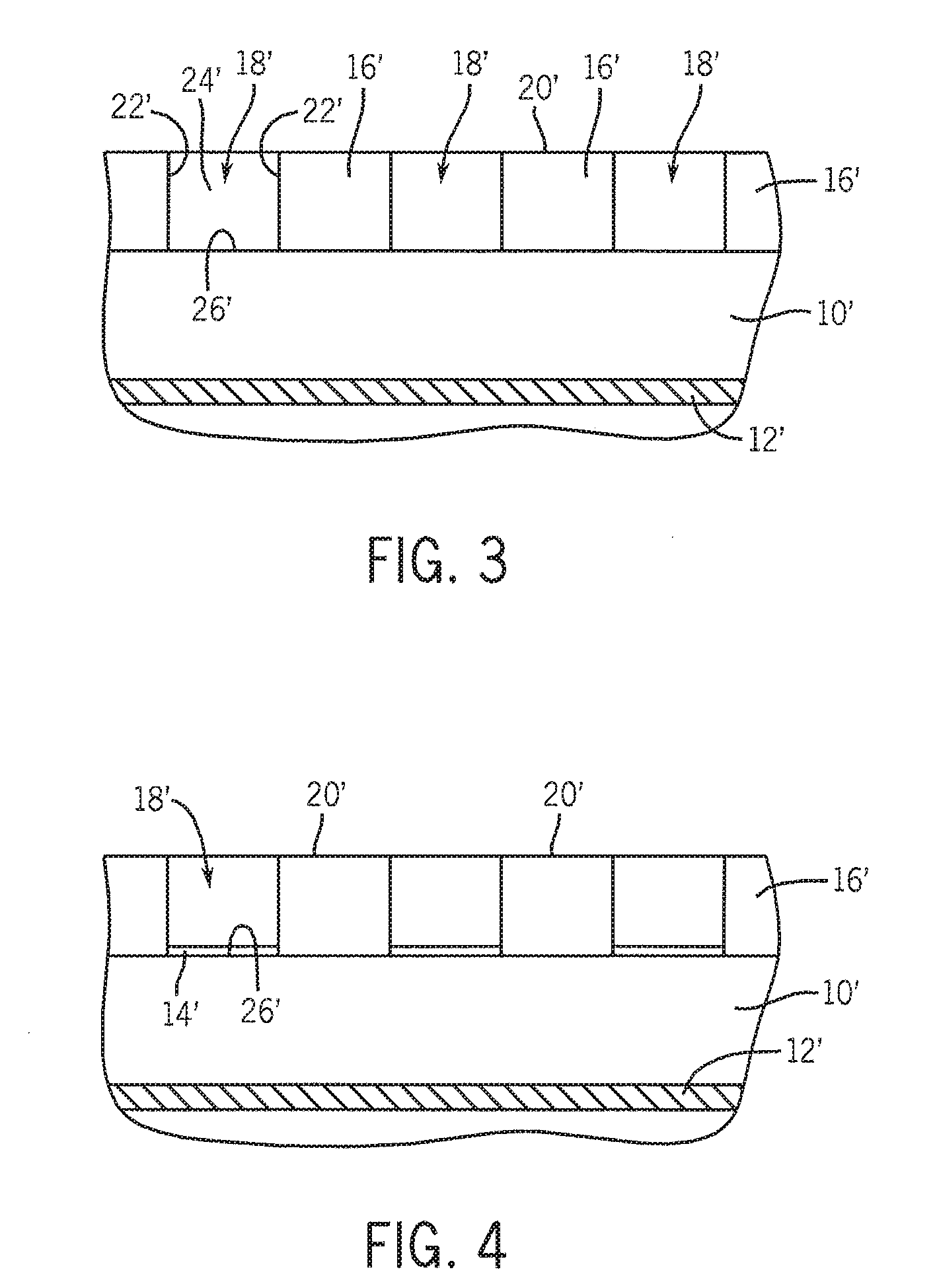
[0011] FIG. 3 illustrates a side elevational view of a portion of a substrate at a preliminary processing stage according to another embodiment of the disclosure, showing the substrate with trenches in a material layer formed on the substrate.
[0012] FIG. 4 illustrates a side elevational view of the substrate of FIG. 3 at a subsequent stage showing the formation of a neutral wetting material within the trenches.
[0013] FIG. 5 is a diagrammatic top plan view of the substrate of FIG. 2 at a subsequent stage showing a block copolymer material within the trenches. FIGS. 5A and 5B illustrate elevational, cross-sectional views of a portion of the substrate depicted in FIG. 5 taken along lines 5A-5A and 5B-5B, respectively.
[0014] FIGS. 6-8 are diagrammatic top plan views of the substrate of FIG. 5 at subsequent stages showing annealing of a portion of the film according to an embodiment of the invention by a zoned annealing technique. FIGS. 6A-8A illustrate elevational, cross-sectional views of the substrate depicted in FIGS. 6-8 taken along lines 6A-6A, 7A-7A and 8A-8A, respectively, showing an embodiment of a heating device for zone annealing the film. FIG. 6B is an elevational, cross-sectional view of the substrate depicted in FIG. 6 taken along lines 6B-6B.
[0015] FIG. 9 is a top plan view of the substrate of FIG. 5 at a subsequent stage according to another embodiment of a method of the invention, illustrating placement of a non-preferential wetting material over the block copolymer material during an anneal. FIGS. 9A and 9B are elevational, cross-sectional views of the substrate depicted in FIG. 9 taken along lines 9A-9A and 9B-9B, respectively.
[0016] FIGS. 10A and 10B are cross-sectional views of the substrate shown in FIGS. 9A and 9B, respectively, at a subsequent stage showing the annealed, self-assembled block copolymer material, and removal of the non-preferential wetting material after the anneal.
[0017] FIGS. 11-13 are top plan views of the substrate of FIG. 8 at subsequent stages, illustrating an embodiment of the use of the self-assembled block copolymer film after removal of one of the polymer blocks, as a mask to etch the substrate and filling of the etched openings.
[0018] FIGS. 11A-13A illustrate elevational, cross-sectional views of a portion of the substrate depicted in FIGS. 11-13 taken along lines 11A-11A to 13A-13A, respectively.
[0019] FIGS. 11B-13B are cross-sectional views of the substrate depicted in FIGS. 11-13 taken along lines 11B-11B to 13B-13B, respectively.
DETAILED DESCRIPTION OF THE INVENTION
[0020] The following description with reference to the drawings provides illustrative examples of devices and methods according to embodiments of the invention. Such description is for illustrative purposes only and not for purposes of limiting the same.
[0021] In the context of the current application, the terms "semiconductor substrate," or "semiconductive substrate," or "semiconductive wafer fragment," or "wafer fragment," or "wafer," will be understood to mean any construction comprising semiconductor material including, but not limited to, bulk semiconductive materials such as a semiconductor wafer (either alone or in assemblies comprising other materials thereon), and semiconductive material layers (either alone or in assemblies comprising other materials). The term "substrate" refers to any supporting structure including, but not limited to, the semiconductive substrates, wafer fragments or wafers described above.
[0022] "L.sub.o" as used herein is the inherent periodicity or pitch value (bulk period or repeat unit) of structures that self-assemble upon annealing from a self-assembling (SA) block copolymer. "L.sub.B" as used herein is the periodicity or pitch value of a blend of a block copolymer with one or more of its constituent homopolymers. "L" is used herein to indicate the center-to-center cylinder pitch or spacing of cylinders of the block copolymer or blend, and is equivalent to "L.sub.o" for a pure block copolymer and "L.sub.B" for a copolymer blend.
[0023] In embodiments of the invention, a polymer material (e.g., film, layer) is prepared by guided self-assembly of block copolymers, with both polymer domains at the air interface. The block copolymer material spontaneously assembles into periodic structures by microphase separation of the constituent polymer blocks after annealing, forming ordered domains of perpendicular-oriented cylinders at nanometer-scale dimensions within a trench.
[0024] A method for fabricating a self-assembled block copolymer material that defines a one-dimensional (1D) array of nanometer-scale, perpendicular-oriented cylinders according to an embodiment of the invention is illustrated with reference to FIGS. 1-8.
[0025] The described embodiment involves a thermal anneal of a cylindrical-phase block copolymer under a solvent atmosphere. The anneal is conducted in combination with a graphoepitaxy technique that utilizes a lithographically defined trench as a guide with a floor composed of a material that is neutral wetting to both polymer blocks, and sidewalls and ends that are preferential wetting to one polymer block and function as constraints to induce the block copolymer to self-assemble into an ordered 1D array of a single row of cylinders in a polymer matrix oriented perpendicular to the trench floor and registered to the trench sidewalls. In some embodiments, two or more rows of perpendicular-oriented cylinders can be formed in each trench.
[0026] As depicted in FIGS. 1-1B, a substrate 10 is provided, which can be silicon, silicon oxide, silicon nitride, silicon oxynitride, silicon oxycarbide, among other materials. As further depicted, conductive lines 12 (or other active area, e.g., semiconducting regions) are situated within the substrate 10.
[0027] In any of the described embodiments, a single trench or multiple trenches can be formed in the substrate, and can span the entire width of an array of lines (or other active area). In embodiments of the invention, the substrate 10 is provided with an array of conductive lines 12 (or other active areas) at a pitch of L. The trench or trenches are formed over the active areas 12 (e.g., lines) such that when the block copolymer material is annealed, each cylinder will be situated above a single active area 12 (e.g., a conductive line). In some embodiments, multiple trenches 18 are formed with the ends 24 of each adjacent trench 18 aligned or slightly offset from each other at less than 5% of L such that cylinders in adjacent trenches 18 are aligned and situated above the same conductive line 12.
[0028] In the illustrated embodiment, a neutral wetting material 14 (e.g., random copolymer) has been formed over the substrate 10. A material layer 16 (or one or more material layers) can then be formed over the neutral wetting material 14 and etched to form trenches 18 that are oriented perpendicular to the array of conductive lines 12, as shown in FIGS. 2-2B. Portions of the material layer 16 form a spacer 20 outside and between the trenches. The trenches 18 are structured with opposing sidewalls 22, opposing ends 24, a floor 26, a width (w.sub.t), a length (l.sub.t) and a depth (D.sub.t).
[0029] In another embodiment, the material layer 16' can be formed on the substrate 10', etched to form the trenches 18' as depicted in FIG. 3, and a neutral wetting material 14' can then be formed on the trench floors 26' as shown in FIG. 4. For example, a random copolymer material can be deposited into the trenches 18' and crosslinked to form a neutral wetting material layer. Material on surfaces outside the trenches 18' such as on the spacers 20' (e.g., non-crosslinked random copolymer) can be subsequently removed.
[0030] Single or multiple trenches 18 (as shown) can be formed using a lithographic tool having an exposure system capable of patterning at the scale of L (10-100 nm). Such exposure systems include, for example, extreme ultraviolet (EUV) lithography, proximity X-rays and electron beam (E-beam) lithography, as known and used in the art. Conventional photolithography can attain (at smallest) about 58 nm features.
[0031] A method called "pitch doubling" or "pitch multiplication" can also be used for extending the capabilities of photolithographic techniques beyond their minimum pitch, as described, for example, in U.S. Pat. No. 5,328,810 (Lowrey et al.), U.S. Pat. No. 7,115,525 (Abatchev, et al.), U.S. Patent Publication 2006/0281266 (U.S. Pat. No. 7,396,781, issued Jul. 8, 2008, to Wells) and U.S. Patent Publication 2007/0023805 (U.S. Pat. No. 7,776,715, issued Aug. 17, 2010, to Wells). Briefly, a pattern of lines is photolithographically formed in a photoresist material overlying a layer of an expendable material, which in turn overlies a substrate, the expendable material layer is etched to form placeholders or mandrels, the photoresist is stripped, spacers are formed on the sides of the mandrels, and the mandrels are then removed, leaving behind the spacers as a mask for patterning the substrate. Thus, where the initial photolithography formed a pattern defining one feature and one space, the same width now defines two features and two spaces, with the spaces defined by the spacers. As a result, the smallest feature size possible with a photolithographic technique is effectively decreased down to about 30 nm or less.
[0032] Factors in forming a single 1D array or layer of perpendicular-oriented nanocylinders within the trenches include the width (w.sub.t) and depth (D.sub.t) of the trench, the formulation of the block copolymer or blend to achieve the desired pitch (L), and the thickness (t) of the block copolymer material within the trench.
[0033] There is a shift from two rows to one row of the perpendicular cylinders within the center of the trench 18 as the width (w.sub.t) of the trench 18 is decreased and/or the periodicity (L value) of the block copolymer is increased, for example, by forming a ternary blend by the addition of both constituent homopolymers. The boundary conditions of the trench sidewalls 22 in both the x- and y-axis impose a structure wherein each trench 18 contains "n" number of features (e.g., cylinders). For example, a block copolymer or blend having a pitch or L value of 35-nm deposited into a 75-nm wide trench 18 having a neutral wetting floor will, upon annealing, result in a zigzag pattern of 17.5-nm diameter (.about.0.5*L) perpendicular cylinders that are offset by about one-half the pitch distance (about 0.5*L) for the length (l.sub.t) of the trench 18, rather than a single line row of perpendicular cylinders aligned with the sidewalls 22 down the center of the trench 18.
[0034] In the illustrated embodiment, the trenches 18 are constructed with a width (w.sub.t) of about 1.5-2*L (or 1.5-2.times.the pitch value) of the block copolymer such that a cast block copolymer material (or blend) of about L will self-assemble upon annealing into a single row of perpendicular cylinders (diameter.about.0.5*L) with a center-to-center pitch distance (p) of adjacent cylinders at or about L. For example, in using a cylindrical phase block copolymer with an about 50 nm pitch value or L, the width (w.sub.t) of the trenches 18 can be about 1.5-2*50 nm or about 75-100 nm. The length (l.sub.t) of the trenches 18 is at or about n*L or an integer multiple of L, typically within a range of about n*10 to about n*100 nm (with n being the number of features or structures, e.g., cylinders). The depth (D.sub.t) of the trenches 18 is greater than or equal to L (D.sub.t>L). The width of the spacers 20 between adjacent trenches can vary and is generally about L to about n*L. In some embodiments, the trench dimension is about 20-100 nm wide (w.sub.t) and about 100-25,000 nm in length (l.sub.t), with a depth (D.sub.t) of about 10-100 nm.
[0035] A self-assembling, cylindrical-phase block copolymer material 28 having an inherent pitch at or about L.sub.o (or a ternary blend of block copolymer and homopolymers blended to have a pitch at or about L.sub.B) is deposited into the trenches 18, typically as a film (as in FIGS. 5-5B).
[0036] The block copolymer (or blend) is constructed such that all of the polymer blocks will have equal preference for a neutral wetting material on the trench floor. The block copolymer material can be constructed to provide desired properties such as defect tolerance and ease of development and/or removal of one of the blocks. In some embodiments of the invention, the block copolymer or blend is constructed such that the minor domain can be selectively removed.
[0037] Examples of diblock copolymers include, for example, poly(styrene)-b-poly(vinylpyridine) (PS-b-PVP), poly(styrene)-b-poly(methyl methacrylate) (PS-b-PMMA) or other PS-b-poly(acrylate) or PS-b-poly(methacrylate), poly(styrene)-b-poly(lactide) (PS-b-PLA), poly(styrene)-b-poly(tert-butyl acrylate) (PS-b-PtBA), and poly(styrene)-b-poly(ethylene-co-butylene (PS-b-(PS-co-PB)), poly(styrene)-b-poly(ethylene oxide) (PS-b-PEO), poly(isoprene)-b-poly(ethyleneoxide) (PI-b-PEO), poly(isoprene)-b-poly(methyl methacrylate) (PI-b-PMMA), poly(butadiene)-b-poly(ethyleneoxide) (PBD-b-PEO), a PS-b-PEO block copolymer having a cleavable junction such as a triphenylmethyl (trityl) ether linkage between PS and PEO blocks (optionally complexed with a dilute concentration (e.g., about 1 wt %) of a salt such as KCl, KI, LiCl, LiI, CsCl or CsI (Zhang et al., Adv. Mater. 2007, 19, 1571-1576), a PS-b-PMMA block copolymer doped with PEO-coated gold nanoparticles of a size less than the diameter of the self-assembled cylinders (Park et al., Macromolecules, 2007, 40(11), 8119-8124), and a poly(styrene)-b-poly(2-vinylpyridine) (PS-b-P2VP) block copolymer having a cleavable junction such as a dithiol group, among others, with PS-b-PVP used in the illustrated embodiment. Other types of block copolymers (i.e., triblock or multiblock copolymers) can be used. Examples of triblock copolymers include ABC copolymers such as poly(styrene-b-methyl methacrylate-b-ethylene oxide) (PS-b-PMMA-b-PEO), and ABA copolymers, such as PS-PMMA-PS, PMMA-PS-PMMA, and PS-b-PI-b-PS, among others.
[0038] The film morphology, including the domain sizes and periods (L.sub.o) of the microphase-separated domains, can be controlled by chain length of a block copolymer (molecular weight, MW) and volume fraction of the AB blocks of a diblock copolymer to produce cylindrical morphologies (among others). For example, for volume fractions at ratios of the two blocks generally between about 60:40 and 80:20 (A:B), the diblock copolymer will microphase separate and self-assemble into periodic cylindrical domains of polymer B within a matrix of polymer A. An example of a cylinder-forming PS-b-PVP copolymer material (L.sub.o.about.28 nm) to form about 14 nm diameter cylindrical PVP domains in a matrix of PS is composed of about 70 wt % PS and 30 wt % PVP with a total molecular weight (M.sub.n) of 44.5 kg/mol. An example of a cylinder-forming PS-b-PMMA copolymer material (L.sub.o=35 nm) to form about 20 nm diameter cylindrical PMMA domains in a matrix of PS is composed of about 70 wt % PS and 30 wt % PMMA with a total molecular weight (M.sub.n) of 67 kg/mol. As another example, a PS-b-PLA copolymer material (L=49 nm) can be composed of about 71 wt % PS and 29 wt % PLA with a total molecular weight (M.sub.n) of about 60.5 kg/mol to form about 27 nm diameter cylindrical PLA domains in a matrix of PS.
[0039] The L value of the block copolymer can be modified, for example, by adjusting the molecular weight of the block copolymer. The block copolymer material can also be formulated as a binary or ternary blend comprising a block copolymer and one or more homopolymers (HPs) of the same type of polymers as the polymer blocks in the block copolymer, to produce a blend that will swell the size of the polymer domains and increase the L value. The concentration of homopolymers in the blend can range from 0 to about 60 wt %.
[0040] An example of a ternary diblock copolymer blend is a PS-b-P2VP/PS/P2VP blend, for example, 60 wt % of 32.5 K/12 K PS-b-P2VP, 20 wt % of 10 K PS, and 20 wt % of 10 K P2VP. Another example of a ternary diblock copolymer blend is a PS-b-PMMA/PS/PMMA blend, for example, 60 wt % of 46K/21K PS-b-PMMA, 20 wt % of 20K polystyrene and 20 wt % of 20K poly(methyl methacrylate). Yet another example is a blend of 60:20:20 (wt %) of PS-b-PEO/PS/PEO, or a blend of about 85-90 wt % PS-b-PEO and up to 10-15 wt % PEO; it is believed that the added PEO homopolymer may function, at least in part, to lower the surface energy of the PEO domains to that of PS.
[0041] In the present embodiment, the trench floors 26 are structured to be neutral wetting (equal affinity for both blocks of the copolymer) to induce formation of cylindrical polymer domains that are oriented perpendicular to the trench floors 26, and the trench sidewalls 22 and ends 24 are structured to be preferential wetting by one block of the block copolymer to induce registration of the cylinders to the sidewalls 22 as the polymer blocks self-assemble. In response to the wetting properties of the trench surfaces, upon annealing, the preferred or minority block of the cylindrical-phase block copolymer will self-assemble to form a single row of cylindrical domains in the center of a polymer matrix for the length of the trench and segregate to the sidewalls and edges of the trench to form a thin interface brush or wetting layer (e.g., as in FIGS. 6-6B). Entropic forces drive the wetting of a neutral wetting surface by both blocks, and enthalpic forces drive the wetting of a preferential-wetting surface by the preferred block (e.g., the minority block).
[0042] To provide preferential wetting surfaces, for example, in the use of a PS-b-PVP (or PS-b-PMMA, etc.) block copolymer, the material layer 16 can be composed of silicon (with native oxide), oxide (e.g., silicon oxide, SiO.sub.x), silicon nitride, silicon oxycarbide, indium tin oxide (ITO), silicon oxynitride, and resist materials such as methacrylate-based resists and polydimethylglutarimide resists, among other materials, which exhibit preferential wetting toward the PVP (or PMMA, etc.) block. In the use of a PS-b-PVP cylinder-phase block copolymer material, for example, the block copolymer material will self-assemble to form a thin interface layer and cylinders of PVP in a PS matrix.
[0043] In other embodiments, a preferential wetting material such as a polymethyl methacrylate (PMMA) polymer modified with an --OH containing moiety (e.g., hydroxyethylmethacrylate) can be applied onto the surfaces of the trenches, for example, by spin-coating and then heating (e.g., to about 170.degree. C.) to allow the terminal OH groups to end-graft to oxide sidewalls 22 and ends 24 of the trenches 18. Non-grafted material can be removed by rinsing with an appropriate solvent (e.g., toluene). See, for example, Mansky et al., Science, 1997, 275, 1458-1460, and In et al., Langmuir, 2006, 22, 7855-7860.
[0044] A neutral wetting trench floor 26 allows both blocks of the copolymer material to wet the floor 26 of the trench 18. A neutral wetting material 14 can be provided by applying a neutral wetting polymer (e.g., a neutral wetting random copolymer) onto the substrate 10, forming the material layer 16 and then etching the trenches 18 to expose the underlying neutral wetting material, as illustrated in FIGS. 2-2B.
[0045] In another embodiment illustrated in FIGS. 3 and 4, a neutral wetting random copolymer material can be applied after forming the trenches 18', for example, as a blanket coat by casting or spin-coating into the trenches 18', as depicted in FIG. 4. The random copolymer material can then be thermally processed to flow the material into the bottom of the trenches 18' by capillary action, which results in a layer (mat) 14' composed of the crosslinked, neutral wetting random copolymer. In another embodiment, the random copolymer material within the trenches 18' can be photo-exposed (e.g., through a mask or reticle) to crosslink the random copolymer within the trenches 18' to form the neutral wetting material 14'. Non-crosslinked random copolymer material outside the trenches (e.g., on the spacers 20') can be subsequently removed.
[0046] Neutral wetting surfaces can be specifically prepared by the application of random copolymers composed of monomers identical to those in the block copolymer and tailored such that the mole fraction of each monomer is appropriate to form a neutral wetting surface. For example, in the use of a PS-b-PVP block copolymer, a neutral wetting material 14 can be formed from a thin film of a photo-crosslinkable random PS-r-PVP that exhibits non-preferential or neutral wetting toward PS and PVP, which can be cast onto the substrate 10 (e.g., by spin-coating). The random copolymer material can be fixed in place by chemical grafting (on an oxide substrate) or by thermally or photolytically crosslinking (any surface) to form a mat that is neutral wetting to PS and PVP and insoluble when the block copolymer material is cast onto it, due to the crosslinking. In another example, in the use of PS-b-PMMA, a photo-crosslinkable PS-r-PMMA random copolymer (e.g., containing an about 0.6 mole fraction of styrene) can be used.
[0047] In embodiments in which the substrate 10 is silicon (with native oxide), another neutral wetting surface for PS-b-PMMA can be provided by hydrogen-terminated silicon. The floors 26 of the trenches 18 can be etched, for example, with a hydrogen plasma, to remove the oxide material and form hydrogen-terminated silicon, which is neutral wetting with equal affinity for both blocks of a block copolymer material. H-terminated silicon can be prepared by a conventional process, for example, by a fluoride ion etch of a silicon substrate (with native oxide present, about 12-15 .ANG.) by exposure to an aqueous solution of hydrogen fluoride (HF) and buffered HF or ammonium fluoride (NH.sub.4F), by HF vapor treatment, or by a hydrogen plasma treatment (e.g., atomic hydrogen).
[0048] An H-terminated silicon substrate can be further processed by grafting a random copolymer such as PS-r-PVP, PS-r-PMMA, etc. selectively onto the substrate resulting in a neutral wetting surface for the corresponding block copolymer (e.g., PS-b-PVP, PS-b-PMMA, etc.). For example, a neutral wetting layer of a PS-r-PMMA random copolymer can be provided by an in situ free radical polymerization of styrene and methyl methacrylate using a di-olefinic linker such as divinyl benzene, which links the polymer to the surface to produce about a 10-15 nm thick film.
[0049] Referring again to FIGS. 3 and 4, in another embodiment, a neutral wetting random copolymer material 14' can be applied after formation of the material layer 16' and trenches 18', which reacts selectively with the trench floor 26' (composed of the substrate 10' material) and not the trench sidewalls 22' or ends 24' (composed of the material layer 16'). For example, a random copolymer (or appropriate blend of homopolymers with block copolymer surfactant) containing epoxide groups will react selectively to terminal amine functional groups (e.g. --NH-- and --NH.sub.2) on silicon nitride and silicon oxynitride surfaces relative to silicon oxide or silicon. In another example in which the trench floor 26' is silicon or polysilicon and the sidewalls 22' are a material such as an oxide (e.g., SiO.sub.x), the trench floor 26' can be treated to form H-terminated silicon and a random copolymer material 14' (e.g., PS-r-PVP, PS-r-PMMA, etc.) can be formed in situ only at the floor surface.
[0050] In another embodiment, a neutral wetting surface (e.g., for PS-b-PMMA and PS-b-PEO) can be provided by grafting a self-assembled monolayer (SAM) of a trichlorosilane-base SAM such as 3-(para-methoxyphenyl)propyltrichorosilane grafted to oxide (e.g., SiO.sub.2) as described, for example, by D. H. Park, Nanotechnology 18 (2007), p. 355304.
[0051] In a further embodiment, a neutral wetting random copolymer of polystyrene (PS), polymethacrylate (PMMA) with hydroxyl group(s) (e.g., 2-hydroxyethyl methacrylate (P(S-r-MMA-r-HEMA)) (e.g., about 58 wt % PS) can be can be selectively grafted to a substrate 10 (e.g., an oxide) as a neutral wetting material 14 about 5-10 nm thick by heating at about 160.degree. C. for about 48 hours. See, for example, In et al., Langmuir, 2006, 22, 7855-7860.
[0052] In yet another embodiment, a blend of hydroxyl-terminated homopolymers and a corresponding low molecular weight block copolymer can be grafted (covalently bonded) to the substrate to form a neutral wetting interface layer (e.g., about 4-5 nm) for PS-b-PMMA and PS-b-P2VP, among other block copolymers. The block copolymer can function to emulsify the homopolymer blend before grafting. For example, an about 1 wt % solution (e.g., in toluene) of a blend of about 20-50 wt % (or about 30-40 wt %) OH-terminated homopolymers (e.g., M.sub.n=6K) and about 80-50 wt % (or about 70-60 wt %) of a low molecular weight block copolymer (e.g., 5K-5K) can be spin-coated onto a substrate 10 (e.g., SiO.sub.2), heated (baked) (e.g., at 160.degree. C.), and non-grafted (unbonded) polymer material removed, for example, by a solvent rinse (e.g., toluene). For example, the neutral wetting material can be prepared from a blend of about 30 wt % PS-OH (M.sub.n=6K) and PMMA-OH (M.sub.n=6K) (weight ratio of 4:6) and about 70 wt % PS-b-PMMA (5K-5K), or a ternary blend of PS-OH (6K), P2VP-OH (6K) and PS-b-2PVP (8K-8K), etc.
[0053] A surface that is neutral wetting to PS-b-PMMA can also be prepared by spin-coating a blanket layer of a photo- or thermally cross-linkable random copolymer such as a benzocyclobutene- or azidomethylstyrene-functionalized random copolymer of styrene and methyl methacrylate (e.g., poly(styrene-r-benzocyclobutene-r-methyl methacrylate (PS-r-PMMA-r-BCB)). For example, such a random copolymer can comprise about 42 wt % PMMA, about (58-x) wt % PS and x wt % (e.g., about 2-3 wt %) of either polybenzocyclobutene or poly(para-azidomethylstyrene)). An azidomethylstyrene-functionalized random copolymer can be UV photo-crosslinked (e.g., 1-5 MW/cm.sup.2 exposure for about 15 seconds to about 30 minutes) or thermally crosslinked (e.g., at about 170.degree. C. for about 4 hours) to form a crosslinked polymer mat as a neutral wetting material 14. A benzocyclobutene-functionalized random copolymer can be thermally crosslinked (e.g., at about 200.degree. C. for about 4 hours or at about 250.degree. C. for about 10 minutes).
[0054] As illustrated in FIGS. 5-5B, a self-assembling, cylindrical-phase block copolymer material 28 having an inherent pitch at or about L.sub.o (or a ternary blend of block copolymer and homopolymers blended to have a pitch at or about L.sub.B) can be cast or deposited into the trenches 18 to a thickness (t.sub.1) at or about the L value of the block copolymer material 28 (e.g., about .+-.20% of L) such that after annealing (e.g., FIG. 6A), the thickness (t.sub.2) will be at or about the L value and the block copolymer material 28 will self-assemble to form a single layer of cylinders having a diameter of about 0.5*L (e.g., 5-50 nm, or about 20 nm, for example) within a polymer matrix in a single row within each trench 18. The thickness of the block copolymer material 28 can be measured, for example, by ellipsometry techniques.
[0055] The block copolymer material 28 can be deposited by spin-casting (spin-coating) from a dilute solution (e.g., about 0.25-2 wt % solution) of the copolymer in an organic solvent such as dichloroethane (CH.sub.2Cl.sub.2) or toluene, for example. Capillary forces pull excess block copolymer material 28 (e.g., greater than a monolayer) into the trenches 18. As shown, a thin layer or film 28a of the block copolymer material 28 can be deposited onto the material layer 16 outside the trenches 18, e.g., on the spacers 20. Upon annealing, the thin film 28a will flow into the trenches 18 leaving a structureless brush layer on the material layer 16 from a top-down perspective.
[0056] The block copolymer (BCP) material 28 is then heated above its glass transition temperature under a vapor phase containing a partly saturated concentration of an organic solvent to cause the polymer blocks to phase separate and self-assemble according to the preferential and neutral wetting of the trench surfaces to form a self-assembled block copolymer material 30, as illustrated in FIGS. 6-6B. The appropriate partial pressure of solvent vapor to achieve a neutral wetting vapor interface at a particular temperature depends, at least in part, on the block copolymer that is used and can be determined empirically.
[0057] The block copolymer is heated at a thermal anneal temperature that is above its glass transition temperature (T.sub.g) but below the decomposition or degradation temperature (T.sub.d) of the block copolymer material. For example, a PS-b-PVP block copolymer material can be annealed at a temperature of about 150.degree. C.-275.degree. C. in a solvent vapor atmosphere for about 1-24 hours to achieve a self-assembled morphology. A PS-b-PMMA block copolymer material can be annealed at a temperature of about 150.degree. C.-275.degree. C. in a solvent vapor atmosphere for about 1-24 hours to achieve a self-assembled morphology.
[0058] In most applications of a thermal anneal in a vacuum, an air interface is preferentially wetting to one of the polymer domains and the BCP material does not orient into perpendicular structures. In embodiments of the invention, during heating, the BCP material 28 is exposed to solvent vapors of a "good" solvent for both blocks, that is, a neutral organic solvent that solvates both the constituent blocks well.
[0059] In general, solvent annealing consists of two phases. In a first phase, the BCP material is exposed to a solvent vapor that acts to plasticize the film and increase chain mobility causing the domains to intermingle and the loss of order inherent from casting the polymer material. The organic solvent that is utilized is based at least in part on its solubility in the block copolymer material such that sufficient solvent molecules enter the block copolymer material to promote the order-disorder transition of the polymer domains and enable the required molecular rearrangement. Examples of solvents include aromatic solvents such as benzene, toluene, xylene, dimethoxyethane, ethyl acetate, cyclohexanone, etc., and chlorinated solvents such as chloroform, methylene chloride, a chloroform/octane mixture, etc., among others. In a second phase, the substrate is removed from the solvent vapor and the solvent and solvent vapors are allowed to diffuse out of the polymer material and evaporate. The block copolymer material begins to "dry" as the solvent evaporates from the material. The evaporation of the solvent is highly directional and forms a solvent gradient from the "top" (surface) of the BCP material to the "bottom" of the BCP material at the trench floor that induces orientation and self-assembly of structures starting at the air-surface interface, which is neutral wetting due to the partial pressure of solvent at the interface, and driven downward to the floor of the trench, with formation of perpendicular-oriented cylindrical domains 34 guided by the trench sidewalls and extending completely from the air interface to the substrate surface (trench floor).
[0060] In embodiments of the invention, the substrate 10 and BCP material 28 are heated above the boiling point of the solvent such that swelling of the BCP material 28 by the solvent is disallowed.
[0061] The use of a partly-saturated solvent vapor phase above the block copolymer material 28 provides a neutral wetting interface, similar to the second phase of solvent annealing. The concentration of solvent in the air immediate at the vapor interface with the BCP material 28 is maintained at or under saturation to maintain a neutral wetting interface such that both (or all) polymer blocks will equally wet the vapor interface. As both the air and trench floor 26 are neutral wetting, the domains will orient perpendicular throughout the film layer, with the preferential wetting sidewalls inducing lateral order.
[0062] The resulting morphology of the annealed, block copolymer material 30 (e.g., perpendicular orientation of cylinders 34) can be examined, for example, using atomic force microscopy (AFM), transmission electron microscopy (TEM), scanning electron microscopy (SEM), among others.
[0063] In embodiments of the invention, the anneal is performed by globally heating the block copolymer within the trenches in a solvent atmosphere.
[0064] In other embodiments, a zone annealing is conducted to anneal portions or sections of the block copolymer material 28 in trenches on the substrate 10 by a localized application of thermal energy (e.g., heat). Zone annealing can provide rapid self-assembly of the block copolymer material (e.g., on the order of minutes).
[0065] For example, as depicted sequentially in FIGS. 6-8, the substrate 10 (in a vapor atmosphere) and a thermal or heat source 32 (or combined heating and cooling source) can be moved relative to each other (e.g., arrow .rarw.) such that heat is applied above (or underneath) the substrate 10. Only a portion of the BCP material 28 is initially heated above the glass transition temperature and the heated zone is then "pulled" across the substrate 10 (or vice versa). For example, the thermal or heat source 32 can be moved across the substrate 10 at a translational set speed (e.g., about 0.05-10 .mu.m/second using a mechanism such as a motorized translation stage (not shown). Pulling the heated zone across the substrate 10 (or vice versa) can result in faster processing and better ordered structures relative to a global thermal anneal.
[0066] In some embodiments, a hot-to-cold temperature gradient can be provided over (or under) the substrate such that a certain portion of the substrate is heated and then cooled, which can be at a controlled rate. In other embodiments, the substrate can be exposed to a cold-to-hot temperature gradient to anneal the BCP material, followed by cooling.
[0067] In other embodiments, the BCP material can be heated above and then cooled below the order-disorder temperature (but above the glass transition temperature), for example, to remove (melt out) defects and allow the material to recrystallize provided that the order-disorder temperature (T.sub.o-d) is less than the decomposition temperature (T.sub.d) of the block copolymer material. The order-disorder temperature is defined by the temperature dependence of the block copolymer, Chi value, the total number of monomers per chain, and the monomer composition.
[0068] Only those portions of the block copolymer material that are heated above the glass transition temperature (T.sub.g) of the component polymer blocks will self-assemble, and areas of the material that were not sufficiently heated remain disordered and unassembled. For example, as illustrated in FIGS. 6-6B, initially, the block copolymer material 28 within trench 18a can be heated and annealed to form a self-assembled block copolymer material 30 while the unannealed block copolymer material 28 within trenches 18b, 18c remains disordered. Only those portions of the block copolymer material 28 that are heated above the glass transition temperature (T.sub.g) will self-assemble. A next portion of the substrate 10 can then be selectively heated, as shown in FIGS. 7 and 7A, resulting in the self-assembly of the block copolymer material within trench 18b. A subsequent heating of the remaining areas of the substrate 10 can then be conducted, e.g., as depicted in FIGS. 8 and 8A.
[0069] Upon annealing, the cylindrical-phase block copolymer material 28 will self-assemble into a block copolymer material 30 (e.g., film) in response to the character of the block copolymer composition (e.g., PS-b-PVP having an inherent pitch at or about L) and the boundary conditions, including the constraints provided by the width (w.sub.t) of the trench 18 and the wetting properties of the trench surfaces including a trench floor 26 that exhibits neutral or non-preferential wetting toward both polymer blocks (e.g., a random graft copolymer), sidewalls 22 that are preferential wetting by the minority (preferred) block of the block copolymer (e.g., the PVP block), and the presence of a neutral or non-preferential solvent (or in some embodiments, a film or material that is neutral or non-preferential wetting) in contact with the surface of the block copolymer material 28 in the trenches 18. The anneal results in a row (or rows) of perpendicularly oriented cylinders 34 of the minority polymer (preferred) block (e.g., PVP) within a matrix 36 of the majority polymer block (e.g., PS), with the cylinders 34 registered and parallel to the sidewalls 22 of the trenches 18. The diameter of the cylinders 34 will generally be at or about 0.5*L (e.g., about one-half of the center-to-center distance between cylinders). In addition, the minority (preferred) block (e.g., PVP) will segregate to and wet the preferential wetting sidewalls 22 and ends 24 of the trenches 18 to form a thin interface or wetting brush layer 34a having a thickness generally about one-fourth of the center-to-center distance between adjacent cylinders 34. For example, a layer of the PVP block will wet oxide interfaces with attached PS domains directed outward from the oxide material.
[0070] In some embodiments, the self-assembled block copolymer material 30 is defined by a single layer of an array of cylindrical domains (cylinders) 34, each with a diameter at or about 0.5*L (e.g., about one-half of the center-to-center distance between cylinders), with the number (n) of cylinders in the row according to the length (4) of the trench, and the center-to-center distance (pitch distance, p) between each cylinder at or about L.
[0071] Optionally, after the block copolymer material is annealed and ordered, the copolymer material can be treated to crosslink the polymer segments (e.g., the PS segments) to fix and enhance the strength of the self-assembled polymer blocks. The polymers can be structured to inherently crosslink (e.g., upon exposure to ultraviolet (UV) radiation, including deep ultraviolet (DUV) radiation), or one of the polymer blocks of the copolymer material can be formulated to contain a crosslinking agent.
[0072] Generally, the film 28a outside the trenches 18a, 18b, 18c (e.g., on spacers 20) will not be thick enough to result in self-assembly. Optionally, the unstructured thin film 28a can be removed, as illustrated in FIGS. 8 and 8A, for example, by an etch technique or a planarization process to provide an about uniformly flat surface. For example, the trench regions can be selectively exposed through a reticle (not shown) to crosslink only the annealed and self-assembled block copolymer material 30 within the trenches 18a, 18b, 18c, and a wash can then be applied with an appropriate solvent (e.g., toluene) to remove the non-crosslinked portions of the block copolymer material 28 (e.g., on the spacers 20), leaving the registered self-assembled block copolymer material 30 within the trenches 18a, 18b, 18c and exposing the surface of the material layer 16 above/outside the trenches 18a, 18b, and 18c. In another embodiment, the annealed, block copolymer material 30 can be crosslinked globally, a photoresist material can be applied to pattern and expose the areas of the block copolymer material 28a outside the trench regions, and the exposed portions of the block copolymer material 28a can be removed, for example, by an oxygen (O.sub.2) plasma treatment.
[0073] Referring to FIG. 9, in another embodiment of a method of the invention, a thermal anneal is conducted while applying a non-preferentially wetting material 37' to the surface of the block copolymer (BCP) material 28' in the trenches. In some embodiments, the non-preferentially wetting material 37' is composed of a solid material, which can be physically placed onto the BCP material 28', for example, a soft, flexible or rubbery solid material such as a cross-linked, poly(dimethylsiloxane) (PDMS) elastomer (e.g., SYLGARD.RTM. 184 by Dow-Corning) or other elastomeric polymer material (e.g., silicones, polyurethanes, etc.), which provides an external surface that is neutral wetting. The solid material can be derivatized (e.g., by grafting a random copolymer) such that it presents a neutral wetting surface.
[0074] With the non-preferentially wetting material 37' in contact with the surface of the block copolymer material 28', a thermal annealing process is conducted (arrows .dwnarw.) FIGS. 9A and 9B) to cause the polymer blocks to phase separate in response to the preferential and neutral wetting of the trench surfaces and the non-preferential (neutral) wetting of the overlying material 37', and form a self-assembled block copolymer material 30' as illustrated in FIGS. 10A and 10B.
[0075] After annealing, the non-preferentially wetting material 37' can be removed from contact with the annealed, block copolymer material 30' (arrow .uparw.) as depicted in FIG. 10A. A PDMS or other elastomeric material layer can be removed, for example, by lifting or peeling the material from the surface of the annealed, block copolymer material 30'. Additionally, a solvent such as water, alcohols, and the like, which is compatible with and does not dissolve the block copolymer material 30', can be applied (e.g., by soaking) to permeate and swell the elastomeric material (e.g., PDMS) to enhance physical removal. A dilute fluoride solution (e.g., NH.sub.4F, HF, NaF, etc.) can also be applied to etch and dissolve a PDMS material to remove it from the annealed polymer material.
[0076] Following self-assembly, the pattern of perpendicular-oriented cylinders 34' that is formed on the substrate 10' can then be further processed as desired, for example, to form an etch mask for patterning nanosized features into the underlying substrate 10' through selective removal of one block of the self-assembled block copolymer. Since the domain sizes and periods (L) involved in this method are determined by the chain length of a block copolymer (MW), resolution can exceed other techniques such as conventional photolithography. Processing costs using the technique is significantly less than extreme ultraviolet (EUV) photolithography, which has comparable resolution.
[0077] For example, as illustrated in FIGS. 11-11B, in one embodiment, an etch mask 38 can be formed by selectively removing the cylindrical polymer domains 34 of the self-assembled block copolymer material 30 to produce openings 40 in the polymer matrix 36 (e.g., PS) to expose the underlying substrate 10 at the trench floors 26. For example, the cylindrical domains 34 can be removed by a selective wet etch (e.g., PMMA and PLA by UV exposure/acetic acid development, PLA by aqueous methanol mixture containing sodium hydroxide, PEO by aqueous hydroiodic acid or water, etc.) or by a selective reactive ion etch (ME) process. In embodiments in which the block copolymer includes a cleavable linker group, the film can be exposed to a solvent selective to the minor domain, for example, an alcohol for PVP, water for PEO or PLA, and acetic acid for PMMA, that contains a cleaving agent to remove (e.g., wash out) the minor domain. As depicted in FIGS. 12-12B, the remaining porous polymer (e.g., PS) matrix 36 can then be used as a lithographic template or mask to etch (arrows .dwnarw..dwnarw.) a series of cylindrical-shaped openings or contact holes 42 in the nanometer size range (e.g., about 10-100 nm) to the conductive lines 12 or other active area (e.g., semiconducting region, etc.) in the underlying substrate 10 (or an underlayer). The openings 42 can be formed, for example, using a selective reactive ion etching (RIE) process.
[0078] Further processing can then be performed as desired. For example, as depicted in FIGS. 13-13B, the residual polymer matrix 36 can be removed (e.g., PS by an oxidation process such as a plasma O.sub.2 etch) and the openings 42 of substrate 10 can be filled with a material 44 such as a metal or metal alloy such as Cu, Al, W, Si, and Ti.sub.3 N.sub.4, among others, to form arrays of cylindrical contacts to the conductive lines 12. The cylindrical openings 42 in the substrate 10 can also be filled with a metal-insulator-metal stack to form capacitors with an insulating material such as SiO.sub.2, Al.sub.2O.sub.3, HfO.sub.2, ZrO.sub.2, SrTiO.sub.3, and the like.
[0079] Embodiments of the invention utilize a thermal anneal process in combination with solvent annealing, which can provide faster processing than with a solvent anneal alone and expands the types of block copolymers (BCPs) that can be processed to substantially all BCPs. In embodiments using a zone annealing in combination with an organic solvent atmosphere, a wide range of block copolymers can be processed to form perpendicular-oriented nanostructures (e.g., cylinders) and at a rapid rate.
[0080] In addition, methods of the disclosure provide a means of generating self-assembled diblock copolymer films composed of perpendicular-oriented cylinders in a polymer matrix. The methods provide ordered and registered elements on a nanometer scale that can be prepared more inexpensively than by electron beam lithography, EUV photolithography or conventional photolithography. The feature sizes produced and accessible by this invention cannot be easily prepared by conventional photolithography. The described methods and systems can be readily employed and incorporated into existing semiconductor manufacturing process flows and provide a low cost, high-throughput technique for fabricating small structures.
[0081] Although specific embodiments have been illustrated and described herein, it will be appreciated by those of ordinary skill in the art that any arrangement that is calculated to achieve the same purpose may be substituted for the specific embodiments shown. This application is intended to cover any adaptations or variations that operate according to the principles of the invention as described. Therefore, it is intended that this invention be limited only by the claims and the equivalents thereof. The disclosures of patents, references and publications cited in the application are incorporated by reference herein.
* * * * *
D00000
D00001
D00002
D00003
D00004
D00005
D00006
D00007
D00008
D00009
D00010
D00011
D00012

D00013

D00014

D00015

D00016

D00017

XML
uspto.report is an independent third-party trademark research tool that is not affiliated, endorsed, or sponsored by the United States Patent and Trademark Office (USPTO) or any other governmental organization. The information provided by uspto.report is based on publicly available data at the time of writing and is intended for informational purposes only.
While we strive to provide accurate and up-to-date information, we do not guarantee the accuracy, completeness, reliability, or suitability of the information displayed on this site. The use of this site is at your own risk. Any reliance you place on such information is therefore strictly at your own risk.
All official trademark data, including owner information, should be verified by visiting the official USPTO website at www.uspto.gov. This site is not intended to replace professional legal advice and should not be used as a substitute for consulting with a legal professional who is knowledgeable about trademark law.