Semiconductor Device
Hsu; Hsiao-Lin ; et al.
U.S. patent application number 16/200670 was filed with the patent office on 2019-04-11 for semiconductor device. The applicant listed for this patent is UNITED MICROELECTRONICS CORP.. Invention is credited to Hsiao-Lin Hsu, En-Chiuan Liou.
| Application Number | 20190109050 16/200670 |
| Document ID | / |
| Family ID | 64736649 |
| Filed Date | 2019-04-11 |


| United States Patent Application | 20190109050 |
| Kind Code | A1 |
| Hsu; Hsiao-Lin ; et al. | April 11, 2019 |
SEMICONDUCTOR DEVICE
Abstract
A semiconductor device includes a substrate having a fin structure extending along a first direction. The fin structure protrudes from a top surface of a trench isolation region and has a first height. A plurality of gate lines including a first gate line and a second gate line extend along a second direction and striding across the fin structure. The first gate line has a discontinuity directly above a gate cut region. The second gate line is disposed in proximity to a dummy fin region, and does not overlap with the dummy fin region. The fin structure has a second height within the dummy fin region, and the second height is smaller than the first height.
| Inventors: | Hsu; Hsiao-Lin; (Yunlin County, TW) ; Liou; En-Chiuan; (Tainan City, TW) | ||||||||||
| Applicant: |
|
||||||||||
|---|---|---|---|---|---|---|---|---|---|---|---|
| Family ID: | 64736649 | ||||||||||
| Appl. No.: | 16/200670 | ||||||||||
| Filed: | November 27, 2018 |
Related U.S. Patent Documents
| Application Number | Filing Date | Patent Number | ||
|---|---|---|---|---|
| 15806295 | Nov 7, 2017 | 10170369 | ||
| 16200670 | ||||
| Current U.S. Class: | 1/1 |
| Current CPC Class: | H01L 21/823431 20130101; H01L 27/0886 20130101; H01L 29/7855 20130101; H01L 29/7856 20130101; H01L 29/401 20130101; H01L 21/823437 20130101; H01L 29/66545 20130101; H01L 29/785 20130101; H01L 21/823481 20130101 |
| International Class: | H01L 21/8234 20060101 H01L021/8234; H01L 27/088 20060101 H01L027/088; H01L 29/78 20060101 H01L029/78 |
Foreign Application Data
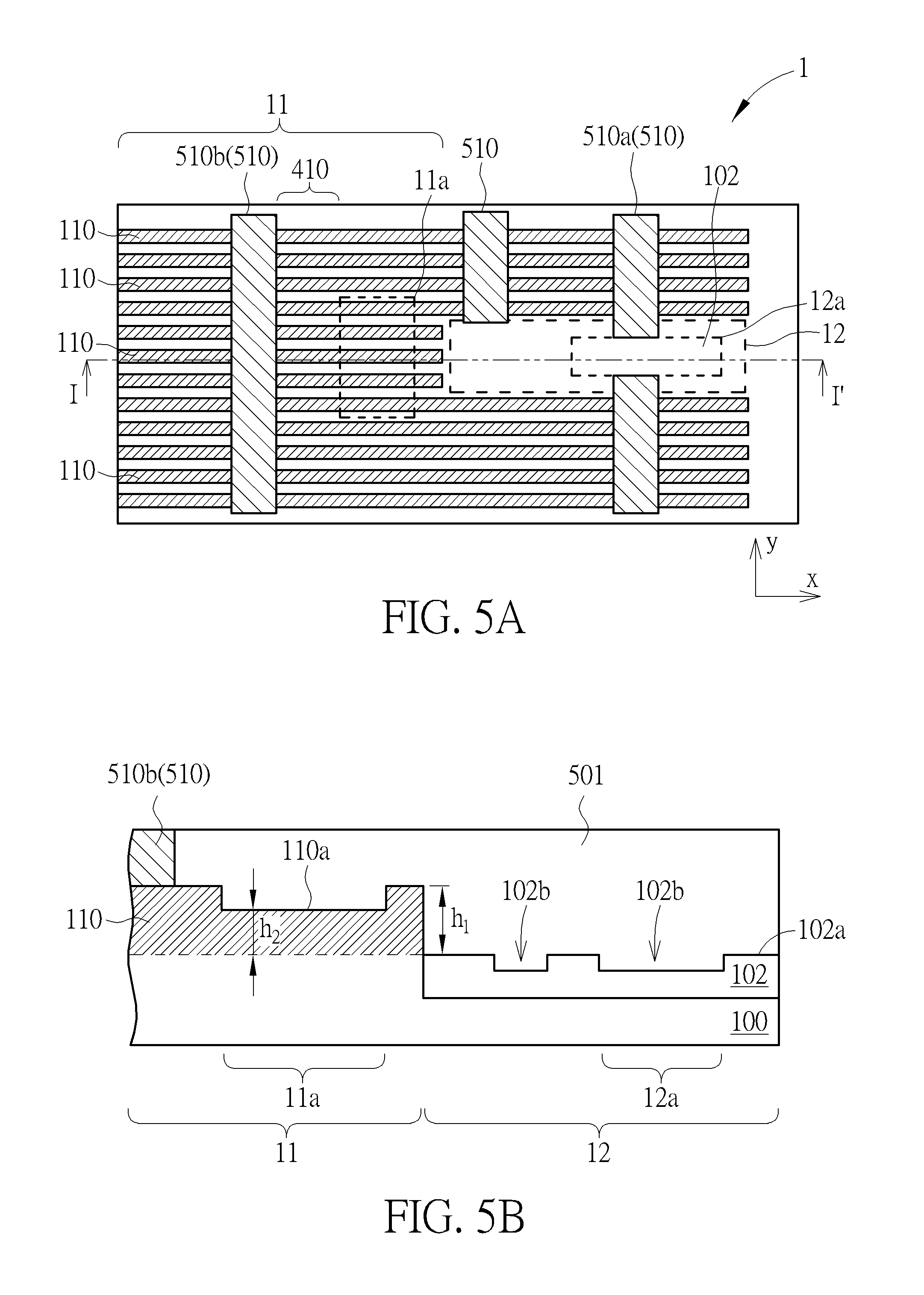
| Date | Code | Application Number |
|---|---|---|
| Oct 6, 2017 | TW | 106134510 |
Claims
1. A semiconductor device, comprising: a substrate having thereon a trench isolation region and a fin structure extending along a first direction, wherein the fin structure protrudes from a top surface of the trench isolation region and has a first height; and a plurality of gate lines comprising a first gate line and a second gate line extending along a second direction and striding across the fin structure, wherein the first gate line has a discontinuity directly above a gate cut region, and the second gate line is disposed in proximity to a dummy fin region, and does not overlap with the dummy fin region, wherein the fin structure has a second height within the dummy fin region, and the second height is smaller than the first height.
2. The semiconductor device according to claim 1, wherein a recess is disposed in the trench isolation region within the gate cut region.
3. The semiconductor device according to claim 1, wherein the gate cut region is completely overlapped with the trench isolation region and does not overlap with the fin structure.
4. The semiconductor device according to claim 1, wherein a top surface of the fin structure within the dummy fin region is higher than the top surface of the trench isolation region.
Description
CROSS REFERENCE TO RELATED APPLICATIONS
[0001] This is a division of U.S. application Ser. No. 15/806,295 filed Nov. 7, 2017, which is included in its entirety herein by reference.
BACKGROUND OF THE INVENTION
1. Field of the Invention
[0002] The present invention relates to the field of semiconductor technology, and in particular to a FinFET semiconductor device and a method for fabricating the same.
2. Description of the Prior Art
[0003] In recent years, due to the miniaturization of various consumer electronic products, the size of the semiconductor devices must be minimized to meet the high degree of integration, high performance, low power consumption and a variety of product requirements. However, with the miniaturization of electronic products, the existing planar field effect transistor (planar FET) has been gradually filed to meet the requirements of the product. Thus, non-planar field-effect transistors such as fin-type field effect transistors (FinFETs) have been developed in the art to achieve high drive currents and to alleviate short channel effects.
[0004] It is known that the FinFETs can be fabricated using a slot-cut first process in which a cut-off region of a poly line is pre-formed in a polysilicon layer overlying the fin structure, and then the lithography process and etching process are performed to pattern the polysilicon layer to thereby form the poly line. However, the prior art slot-cut first process results in a loading effect when coating the organic dielectric layer (ODL), which affects the yield of the process. Therefore, there is still a need for an improved manufacturing method in this field.
SUMMARY OF THE INVENTION
[0005] The main object of the present invention is to provide an improved semiconductor device and a method for fabricating the same, which can solve the disadvantages and shortcomings of the prior art.
[0006] According to one aspect of the invention, a method for fabricating a semiconductor device is disclosed. A substrate having thereon a trench isolation region and a plurality of fin structures extending along a first direction is provided. The plurality of fin structures protrude from a top surface of the trench isolation region. A polysilicon layer is deposited over the substrate. A poly cut opening and a dummy opening are formed in the polysilicon layer. An organic dielectric layer (ODL) is coated over the substrate. The ODL fills into the poly cut opening and the dummy opening. A hard mask layer is deposited on the ODL. A plurality of photoresist line patterns comprising a first photoresist line pattern and a second photoresist line pattern are formed. The photoresist line patterns extend along a second direction on the hard mask layer. The first photoresist line pattern overlaps with the poly cut opening. The second photoresist line pattern is disposed in proximity to the dummy opening, and does not overlap with the dummy opening. The photoresist line patterns are transferred to the polysilicon layer, thereby forming a plurality of poly lines extending along the second direction.
[0007] According to another aspect of the invention, a semiconductor device includes a substrate having a fin structure extending along a first direction. The fin structure protrudes from a top surface of a trench isolation region and has a first height. A plurality of gate lines including a first gate line and a second gate line extend along a second direction and striding across the fin structure. The first gate line has a discontinuity directly above a gate cut region. The second gate line is disposed in proximity to a dummy fin region, and does not overlap with the dummy fin region. The fin structure has a second height within the dummy fin region, and the second height is smaller than the first height.
[0008] These and other objectives of the present invention will no doubt become obvious to those of ordinary skill in the art after reading the following detailed description of the preferred embodiment that is illustrated in the various figures and drawings.
BRIEF DESCRIPTION OF THE DRAWINGS
[0009] FIG. 1A is a schematic top view showing a semiconductor substrate after the formation of fin structures and after the blanket deposition of a polysilicon layer according to one embodiment of the invention.
[0010] FIG. 1B is a schematic, cross-sectional view taken along line I-I' in FIG. 1A.
[0011] FIG. 2A is a schematic top view showing a semiconductor substrate after the formation of a poly cut opening and dummy openings in the polysilicon layer according to one embodiment of the invention.
[0012] FIG. 2B is a schematic, cross-sectional view taken along line I-I' in FIG. 2A.
[0013] FIG. 3A is a schematic top view showing a semiconductor substrate after the formation of photoresist line patterns according to one embodiment of the invention.
[0014] FIG. 3B is a schematic, cross-sectional view taken along line I-I' in FIG. 3A.
[0015] FIG. 4A is a schematic top view showing a semiconductor substrate after the transferring the photoresist line patterns to the underlying polysilicon layer according to one embodiment of the invention.
[0016] FIG. 4B is a schematic, cross-sectional view taken along line I-I' in FIG. 4A.
[0017] FIG.5A is a schematic top view showing a semiconductor substrate after the replacement metal gate (RMG) process according to one embodiment of the invention.
[0018] FIG. 5B is a schematic, cross-sectional view taken along line I-I' in FIG. 5A.
DETAILED DESCRIPTION
[0019] In the following detailed description of the disclosure, reference is made to the accompanying drawings, which form a part hereof, and in which is shown, by way of illustration, specific embodiments in which the invention may be practiced. These embodiments are described in sufficient detail to enable those skilled in the art to practice the invention. Other embodiments maybe utilized and structural changes may be made without departing from the scope of the present disclosure.
[0020] The following detailed description is, therefore, not to be taken in a limiting sense, and the scope of the present invention is defined only by the appended claims, along with the full scope of equivalents to which such claims are entitled. One or more implementations of the present invention will now be described with reference to the attached drawings, wherein like reference numerals are used to refer to like elements throughout, and wherein the illustrated structures are not necessarily drawn to scale.
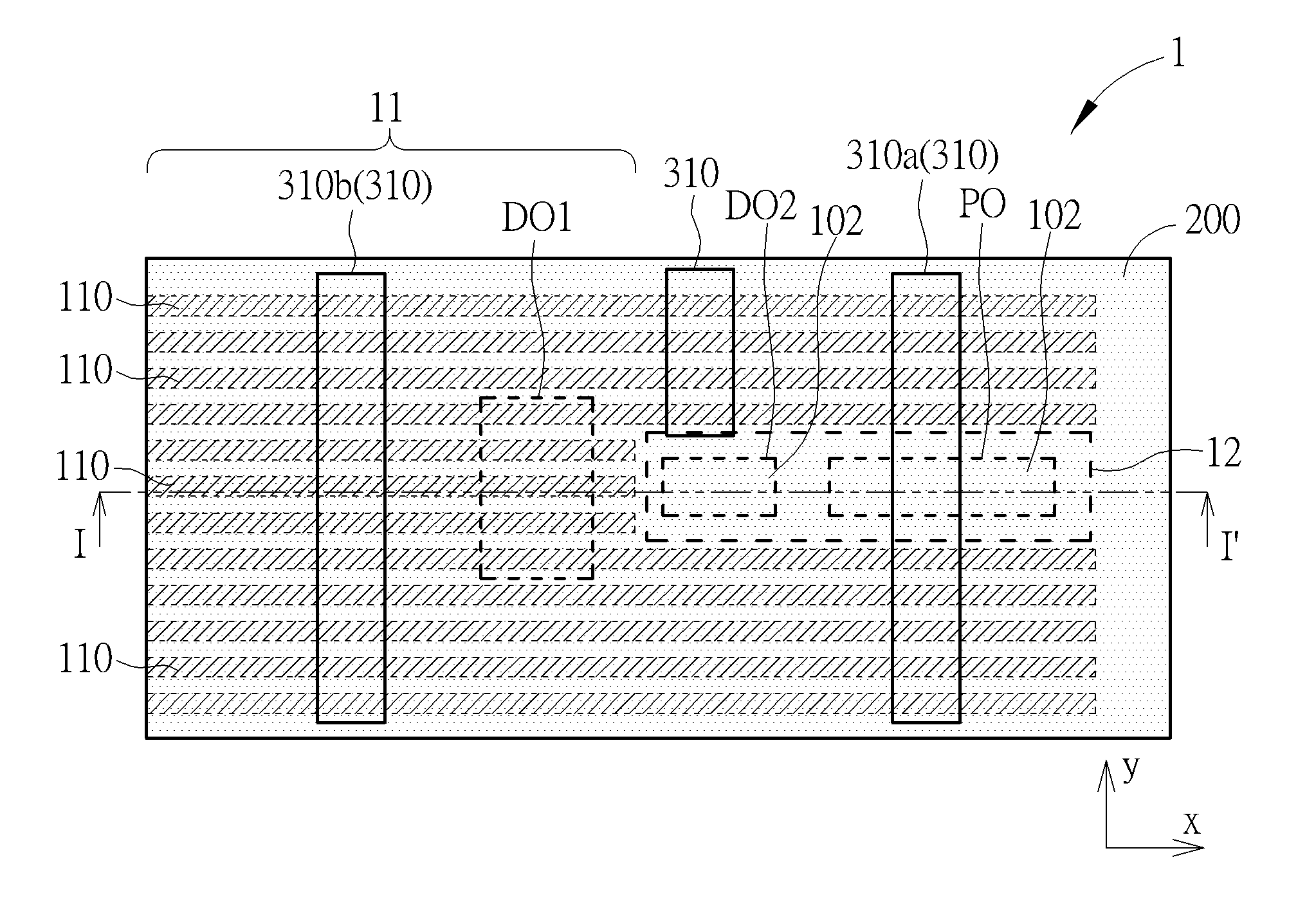
[0021] Please refer FIG. 1A and FIG. 1B. FIG. 1A is a schematic top view showing a semiconductor substrate after the formation of fin structures and after the blanket deposition of a polysilicon layer according to one embodiment of the invention. FIG. 1B is a schematic, cross-sectional view taken along line I-I' in FIG. 1A.
[0022] According to an embodiment of the present invention, the present invention discloses a method of fabricating a semiconductor device 1, for example, the semiconductor device 1 may be a fin-type semiconductor device or a FinFET semiconductor device, but is not limited thereto. First, a trench isolation region 102 and a plurality of fin structures 110 are formed on a substrate 100. According to an embodiment of the present invention, the substrate 100 may be a semiconductor substrate, such as a silicon substrate, but is not limited thereto. The fin structures 110 extend along a first direction (i.e., reference x-axis direction). The fin structures 110 protrude from a top surface 102a of the trench isolation region 102.
[0023] As shown in FIG. 1A, the fin structures 110 form the dense pattern area 11. On the substrate 100, there may be a non-dense region 12 in which only the trench isolation region 102 is formed in the non-dense region 12 and no fin structure 110 is formed within the non-dense region 12.
[0024] According to an embodiment of the present invention, the dense pattern area 11 includes a dummy fin region 11a adjacent to the non-dense region 12. According to an embodiment of the present invention, any circuit element, such as a transistor, a doped region, or a contact element, is not formed on the fin structure 110 of the dummy fin region 11a. According to an embodiment of the present invention, a gate cut region 12a is provided in the non-dense region 12. The gate cut region 12a may completely overlap the trench isolation region 102 without overlapping the fin structures 110, but is not limited thereto.
[0025] According to an embodiment of the present invention, a polysilicon layer 200 is deposited on the substrate 100 in a blanket manner. The polysilicon layer 200 covers the plurality of fin structures 110 within the dense pattern area 11 and the trench isolation region 102 within the non-dense region 12. As can be seen from FIG. 1B, the fin structure 110 protrudes from the top surface 102a of the trench isolation region 102 and has a first height h.sub.1. A step height is formed at the interface between the dense pattern region 11 and the non-dense region 12.
[0026] Please refer FIG. 2A and FIG. 2B. FIG. 2A is a schematic top view showing a semiconductor substrate after the formation of a poly cut opening and dummy openings in the polysilicon layer according to one embodiment of the invention. FIG. 2B is a schematic, cross-sectional view taken along line I-I' in FIG. 2A.
[0027] As shown in FIGS. 2A and 2B, a poly cut opening PO, a dummy opening DO1 and a dummy opening DO2 are formed in the polysilicon layer 200. The poly cut opening PO, dummy openings DO1 and dummy openings DO2 may be formed by using the same lithography process and etching process.
[0028] According to an embodiment of the present invention, the dummy opening DO1 is located directly on the dummy fin region 11a and the dummy opening DO1 exposes the fin structures 110 within the dummy fin region 11a. The poly cut opening PO is directly located on the gate cut region 12a and is completely overlapped with the gate cut region 12a. The dummy opening DO2 is adjacent to the poly cut opening PO and is located directly on the trench isolation region 102.
[0029] According to an embodiment of the present invention, portions of the fin structures 110 within the dummy fin region 11a may be further etched away via the dummy opening DO1 such that the fin structures 110 has a second height h.sub.2 in the dummy fin region 11a, and the second height h.sub.2 is smaller than the first height h.sub.1.
[0030] In addition, the method of the present invention further includes recess etching the trench isolation region 102 via the poly cut opening PO and the dummy opening DO2, thereby forming a recessed structure 102b on the trench isolation region 102 within the gate cut region 12a and the dummy opening DO2.
[0031] According to an embodiment of the present invention, the top surface 110a of the fin structure 110 within the dummy fin region 11a is still higher than the top surface 102a of the trench isolation region 102.
[0032] Please refer FIG. 3A and FIG. 3B. FIG. 3A is a schematic top view showing a semiconductor substrate after the formation of photoresist line patterns according to one embodiment of the invention. FIG. 3B is a schematic, cross-sectional view taken along line I-I' in FIG. 3A.
[0033] As shown in FIGS. 3A and 3B, after the poly cut opening PO, the dummy opening DO1 and the dummy opening DO2 are formed in the polysilicon layer 200, an organic dielectric layer (ODL) 301 is deposited on the substrate 100. The poly cut opening PO and the dummy openings DO1 and DO2 are filled with the ODL 301. Next, a bottom anti-reflective layer 302 may be formed on the ODL 301. Then, a hard mask layer 303 may be deposited on the bottom anti-reflective layer 302, for example, a silicon nitride layer.
[0034] Subsequently, a plurality of photoresist line patterns 310 are formed on the hard mask layer 303, which includes a first photoresist line pattern 310a and a second photoresist line pattern 310b extending in a second direction (i.e., a reference y-axis direction), wherein the first photoresist line pattern 310a overlaps the poly cut opening PO, and the second photoresist line pattern 310b is adjacent to the dummy opening DO1 and does not overlap with the dummy opening DO1. According to an embodiment of the present invention, the plurality of photoresist line patterns 310 are not overlapped with the dummy opening DO1 or the dummy opening DO2.
[0035] Please refer FIG. 4A and FIG. 4B. FIG. 4A is a schematic top view showing a semiconductor substrate after the transferring the photoresist line patterns to the underlying polysilicon layer according to one embodiment of the invention. FIG. 4B is a schematic, cross-sectional view taken along line I-I' in FIG. 4A.
[0036] As shown in FIG. 4A and FIG. 4B, the photoresist line patterns 310 are transferred to the polysilicon layer 200, thereby forming a plurality of poly lines 210 extending in the second direction. The poly lines 210 include a first poly line 210a corresponding to the first photoresist line pattern 310a, wherein the first poly line 210a is cut off or intersected by the poly cut opening PO.
[0037] According to an embodiment of the present invention, the poly lines 210 further comprise a second poly line 210b corresponding to the second photoresist line pattern 310b, wherein the second poly line 210b does not overlap the dummy fin region 11a.
[0038] According to an embodiment of the present invention, a source/drain contact region 410 is provided between the second poly line 210b and the dummy fin region 11a.
[0039] Please refer FIG. 5A and FIG. 5B. FIG.5A is a schematic top view showing a semiconductor substrate after the replacement metal gate (RMG) process according to one embodiment of the invention. FIG. 5B is a schematic, cross-sectional view taken along line I-I' in FIG. 5A.
[0040] As shown in FIGS. 5A and 5B, a dielectric layer 501 is formed on the substrate 100 and planarized. Then, the plurality of poly lines 210 are replaced with a plurality of metal gate lines 510 including a first gate line 510a and a second gate line 510b extending in the second direction and across the fin structures 110 by a replacement metal gate (RMG) process, where the first gate line 510a is discontinuous in the gate cut region 12a and the second gate line 510b is adjacent to the dummy fin region 11a and does not overlap the dummy fin region 11a.
[0041] Those skilled in the art will readily observe that numerous modifications and alterations of the device and method may be made while retaining the teachings of the invention. Accordingly, the above disclosure should be construed as limited only by the metes and bounds of the appended claims.
* * * * *
D00000
D00001
D00002
D00003
D00004
D00005
XML
uspto.report is an independent third-party trademark research tool that is not affiliated, endorsed, or sponsored by the United States Patent and Trademark Office (USPTO) or any other governmental organization. The information provided by uspto.report is based on publicly available data at the time of writing and is intended for informational purposes only.
While we strive to provide accurate and up-to-date information, we do not guarantee the accuracy, completeness, reliability, or suitability of the information displayed on this site. The use of this site is at your own risk. Any reliance you place on such information is therefore strictly at your own risk.
All official trademark data, including owner information, should be verified by visiting the official USPTO website at www.uspto.gov. This site is not intended to replace professional legal advice and should not be used as a substitute for consulting with a legal professional who is knowledgeable about trademark law.