Data Transmission System and Data Transmission Method
PAGANINI; Maurizio ; et al.
U.S. patent application number 16/119988 was filed with the patent office on 2019-04-11 for data transmission system and data transmission method. This patent application is currently assigned to MegaChips Technology America Corporation. The applicant listed for this patent is MegaChips Technology America Corporation. Invention is credited to Rahul Kumar AGARWAL, Ramakrishna CHILUKURI, Alan KOBAYASHI, Maurizio PAGANINI, Sujan Valiyaka THOMAS, Nobuhiro YANAGISAWA.
| Application Number | 20190108148 16/119988 |
| Document ID | / |
| Family ID | 65993245 |
| Filed Date | 2019-04-11 |


| United States Patent Application | 20190108148 |
| Kind Code | A1 |
| PAGANINI; Maurizio ; et al. | April 11, 2019 |
Data Transmission System and Data Transmission Method
Abstract
A data transmission system includes a transmitter having a first switching re-timer and a receiver having a second switching re-timer. The first switching re-timer is configured to double a link rate per lane and halve the number of lanes, and the second switching re-timer is configured to halve the doubled link rate and double the halved number of lanes.
| Inventors: | PAGANINI; Maurizio; (San Jose, CA) ; KOBAYASHI; Alan; (Los Altos, CA) ; CHILUKURI; Ramakrishna; (San Jose, CA) ; AGARWAL; Rahul Kumar; (Saratoga, CA) ; YANAGISAWA; Nobuhiro; (Milpitas, CA) ; THOMAS; Sujan Valiyaka; (Pleasanton, CA) | ||||||||||
| Applicant: |
|
||||||||||
|---|---|---|---|---|---|---|---|---|---|---|---|
| Assignee: | MegaChips Technology America
Corporation San Jose CA |
||||||||||
| Family ID: | 65993245 | ||||||||||
| Appl. No.: | 16/119988 | ||||||||||
| Filed: | August 31, 2018 |
Related U.S. Patent Documents
| Application Number | Filing Date | Patent Number | ||
|---|---|---|---|---|
| 62570879 | Oct 11, 2017 | |||
| Current U.S. Class: | 1/1 |
| Current CPC Class: | H04Q 11/08 20130101; G06F 13/4282 20130101; H04L 25/0272 20130101; G06F 2213/0042 20130101; G06F 13/20 20130101; H04L 25/4908 20130101 |
| International Class: | G06F 13/20 20060101 G06F013/20; G06F 13/42 20060101 G06F013/42; H04Q 11/08 20060101 H04Q011/08; H04L 25/02 20060101 H04L025/02 |
Claims
1. A universal serial bus (USB) transmission device, comprising: a first interface configured to receive display port (DP) data via M lanes at a first link rate, wherein M is a switching re-timer configured to multiplex the DP data received via each of the M lanes into N lanes, wherein N is an integer value equal to M/2; and output the multiplexed data on each of the N lanes at a second link rate, wherein the second link rate is equal to the first link rate multiplied by M/N.
2. The USB transmission device of claim 1, wherein the USB transmission device is USB Type-C compliant transmission device.
3. The USB transmission device of claim 2, wherein the USB transmission device is configured to operate in DP Alt Mode.
4. The USB transmission device of claim 1, wherein the switching re-timer is configured to: receive USB super speed (SS) data via Y lanes at a third link rate; and output the USB SS data via Z lanes at the third link rate, wherein Y is equal to Z.
5. The USB transmission device of claim 1, wherein the N lanes via which the DP data is output and the Z lanes via which the USB SS data is output are output to main link lines of a USB Type-C connector.
6. The USB transmission device of claim 1, wherein the USB transmission device is a USB Type-C connector.
7. The USB transmission device of claim 6, further comprising: four pairs of high-speed differential signal pins.
8. The USB transmission device of claim 7, wherein N equals 2, and the switching re-timer is configured to output the multiplexed data on each of the N lanes via 2 pairs of the high-speed differential signal pins.
9. The USB transmission device of claim 8, wherein the switching re-timer is configured to: receive USB super speed (SS) data via 2 lanes at a third link rate; output the USB SS data via 2 lanes at the third link rate over another two pairs of the high-speed differential signal pins.
10. The USB transmission device of claim 1, wherein M equals 4, and N equals 2.
11. The USB transmission device of claim 10, wherein the switching re-timer is configured to recover a link symbol clock from a clock-to-data recovery circuit.
12. The USB transmission device of claim 11, wherein the switching re-timer is configured to double a speed of the link symbol clock to output the multiplexed data on each of the N lanes at the second link rate.
13. A universal serial bus (USB) reception device, comprising: a first interface configured to receive display port (DP) data via M lanes at a first link rate, wherein M is an integer greater than 1; a switching re-timer configured to demultiplex the DP data received via each of the M lanes into N lanes, wherein N is an integer value equal to M multiplied by 2; and output the multiplexed data on each of the N lanes at a second link rate, wherein the second link rate is equal to the first link rate multiplied by M/N.
14. The USB reception device of claim 13, wherein the USB reception device is USB Type-C compliant reception device.
15. The USB reception device of claim 14, wherein the USB reception device is configured to operate in DP Alt Mode.
16. The USB reception device of claim 13, wherein the switching re-timer is configured to: receive USB super speed (SS) data via Y lanes at a third link rate; and output the USB SS data via Z lanes at the third link rate, wherein Y is equal to Z.
17. The USB reception device of claim 13, wherein the M lanes via which the DP data is received and the Y lanes via which the USB SS data is received correspond to main link lines of a USB Type-C connector.
18. The USB reception device of claim 13, wherein the USB reception device is a USB Type-C connector.
19. The USB reception device of claim 18, further comprising: four pairs of high-speed differential signal pins.
20. The USB reception device of claim 19, wherein M equals 2, and the switching re-timer is configured to receive the DP data on each of the M lanes via 2 pairs of the high-speed differential signal pins.
21. The USB reception device of claim 20, wherein the switching re-timer is configured to: receive USB super speed (SS) data over another two pairs of the high-speed differential signal pins.
22. The USB reception device of claim 13, wherein M equals 2, and N equals 4.
23. The USB reception device of claim 22, wherein the switching re-timer is configured to recover a link symbol clock from a clock-to-data recovery circuit.
24. The USB reception device of claim 23, wherein the switching re-timer is configured to reduce a speed of the link symbol clock in half to output the demultiplexed data on each of the N lanes at the second link rate.
25. A data transmission system comprising: a universal serial bus (USB) transmission device, comprising: a first interface configured to receive display port (DP) data via M lanes at a first link rate, wherein M is an integer greater than 1; a first switching re-timer configured to multiplex the DP data received via each of the M lanes into N lanes, wherein N is an integer value equal to M/2; and output the multiplexed data on each of the N lanes at a second link rate, wherein the second link rate is equal to the first link rate multiplied by M/N; and a USB reception device, comprising: a second interface configured to receive the DP data output from the USB transmission device on Y lanes at the second link rate, wherein Y is an integer greater than 1; a second switching re-timer configured to demultiplex the DP data received via each of the Y lanes into Z lanes, wherein Z is an integer value equal to Y multiplied by 2; and output the multiplexed data on each of the Z lanes at the first link rate.
Description
CROSS-REFERENCE TO RELATED APPLICATIONS
[0001] This application claims the benefit of U.S. Patent Provisional Application No. 62/570,879, filed Oct. 11, 2017, which is herein incorporated by reference in its entirety.
TECHNICAL FIELD
[0002] The present disclosure relates to a data transmission method that has DisplayPort (DP) and Universal Serial Bus Universal Serial Bus (USB) on USB Type-C connector.
BACKGROUND
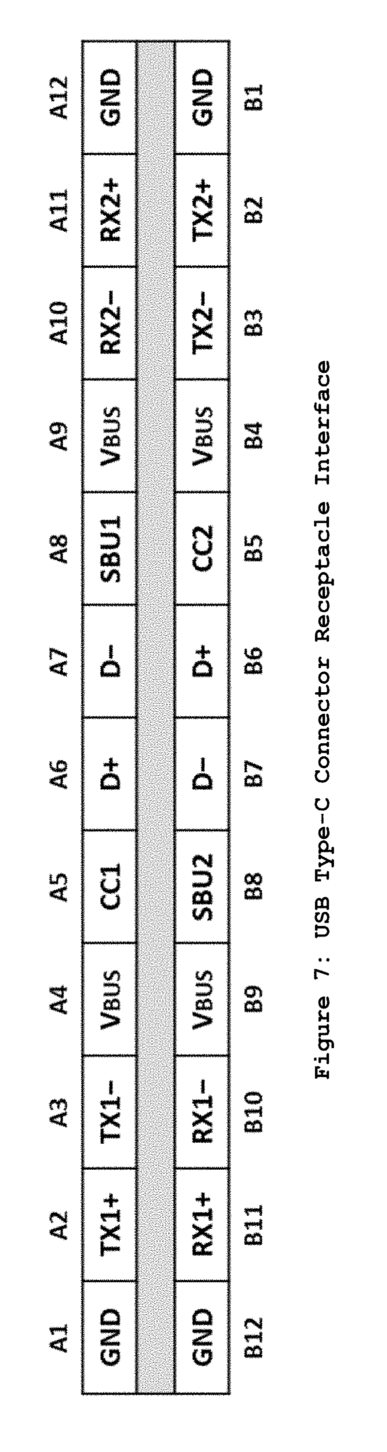
[0003] DP Alt Mode on USB Type-C enables concurrent transport of USB traffic (both USB3.x SS and USB2) and DP traffic over a standard USB Type-C connector. The USB Type-C connector supports 4 pairs of high-speed differential signaling with a bit rate up to 10 Gbps/pair and 2 pairs of pins for a USB2 differential signal (up to 480 Mbps), as depicted in FIG. 7. Only one of the 2 pairs, named A6/A7 and B6/B7 in FIG. 7, of USB2 pins is used for USB2 transport. The pair that is selected depends on the USB Type-C plug connector orientation.
[0004] DP Alt Mode on USB Type-C specification enables either (1) 2 lanes of DP Main Link concurrent with USB3.x SS and USB2 or (2) 4 lanes of DP Main Link concurrent with USB2 without USB3.x SS.
SUMMARY
Problems to be Solved
[0005] For applications such as AR (augmented reality) and VR (virtual reality), there is a growing desire to have the maximum-bandwidth DP transport of 4-lane Main Link at the highest DP link rate of 8.1 Gbps/lane (called HBR3 link rate) concurrent with USB3.1 SS transport. There is one approach that enables this concurrency by routing USB3.1 SS traffic to 2 pairs of USB2 pins on a USB Type-C connector while routing all 4 lanes of DP Main Link to the 4 pairs of high-speed differential signal pins. This approach, however, has the drawbacks as below: [0006] (1) Requires more complex signal multiplexing/routing [0007] (2) Requires tunneling of USB2 traffic through USB3.1 SS traffic [0008] (3) Requires a captive cable with USB Type-C plug connector only on one end
Brief Summary
[0009] The present disclosure describes technology enabling the concurrent transport of USB traffic and DP 4 Lane equivalent traffic over USB Type-C connector without drawbacks such as requirements of more complex signal multiplexing/routing.
[0010] According to one aspect of the present disclosure, a data transmission system includes a transmitter having a first switching re-timer and a receiver having a second switching re-timer. The first switching re-timer is configured to double a link rate per lane and halve the number of lanes, and the second switching re-timer is configured to halve the doubled link rate and double the halved number of lanes.
[0011] According to another aspect of the disclosure, a data transmission system includes a transmitter having a first switching re-timer and a receiver having a second switching re-timer. The first switching re-timer is configured to multiply a link rate per lane by M where M denotes an integer of 2 or more, and multiply the number of lanes by 1/M, and the second switching re-timer is configured to multiply the M-multiplied link rate by 1/M and multiply the 1/M-multiplied number of lanes by M.
BRIEF DESCRIPTION OF THE DRAWINGS
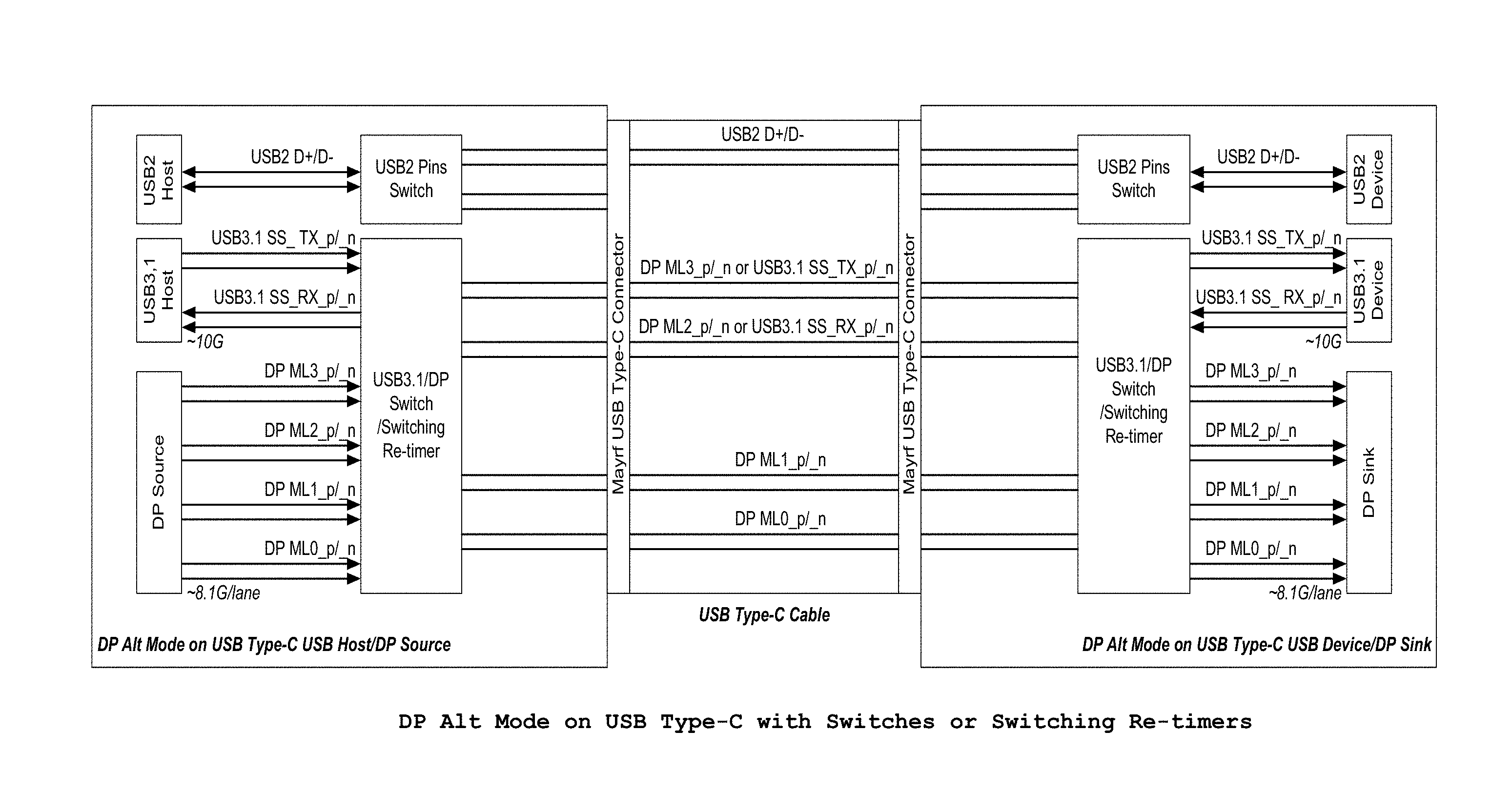
[0012] FIG. 1 illustrates DP Alt Mode on USB Type-C with Switches or Switching Re-timers;
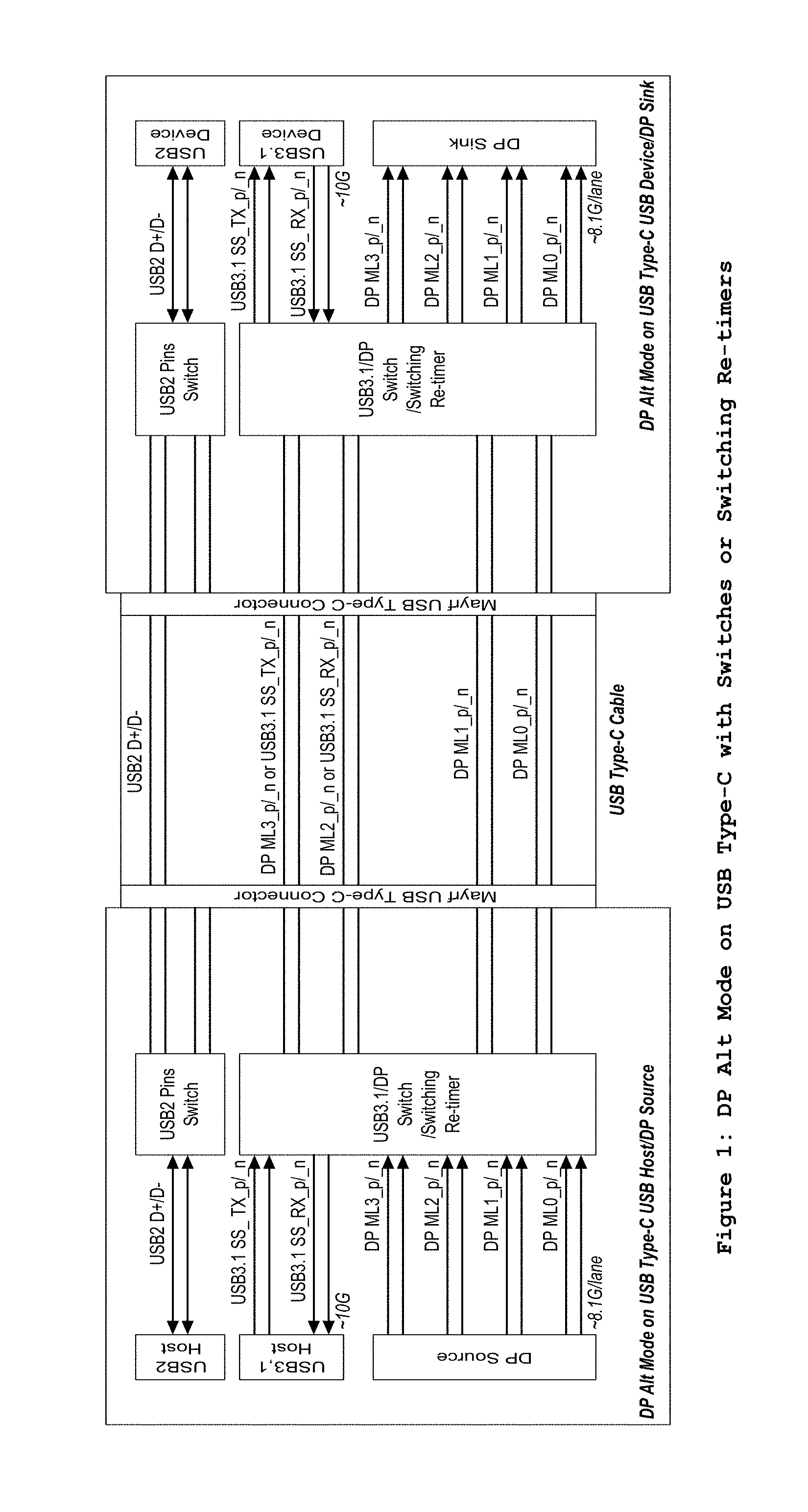
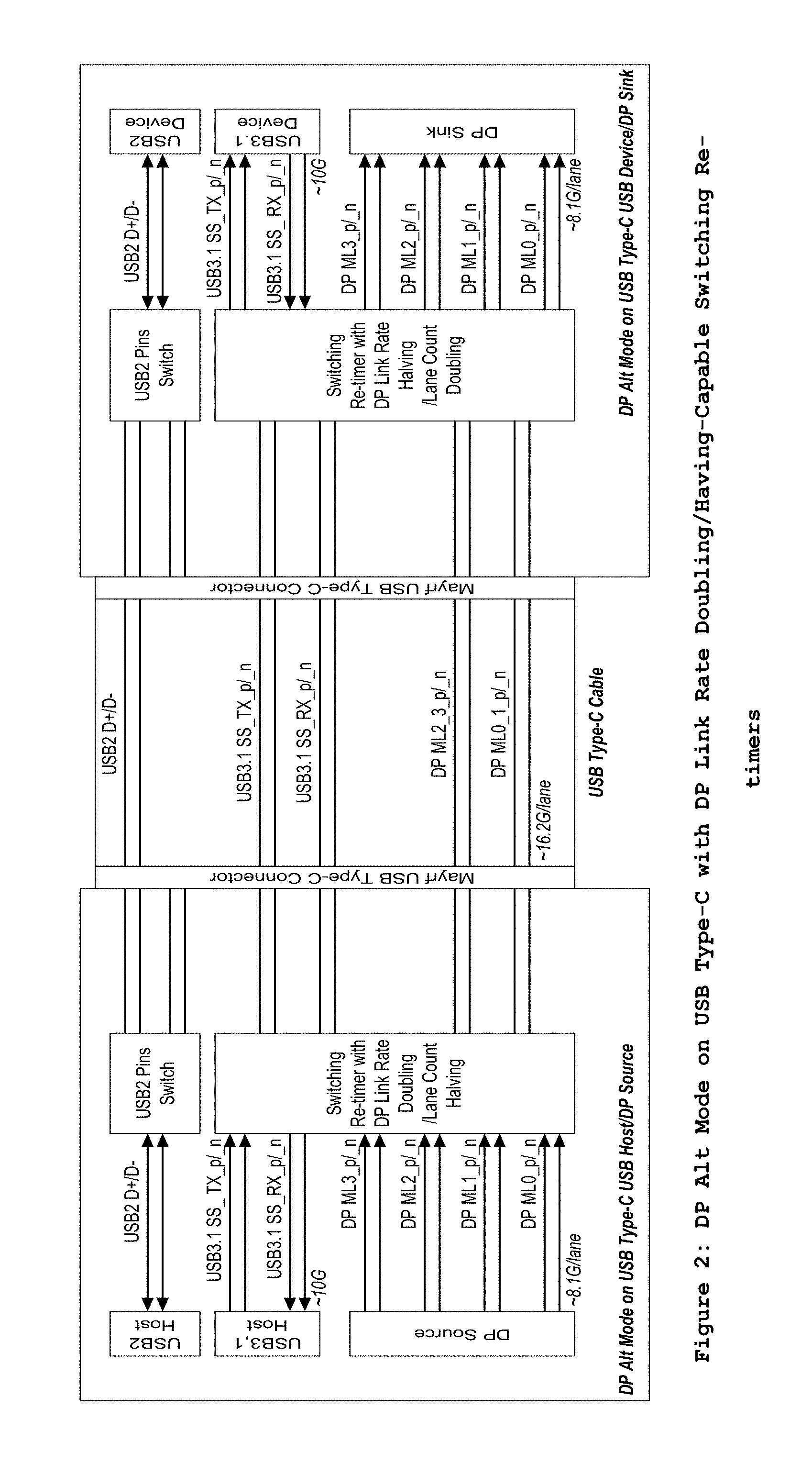
[0013] FIG. 2 illustrates DP Alt Mode on USB Type-C with DP Link Rate Doubling/Having-Capable Switching Re-timers;
[0014] FIG. 3 illustrates Internal Paths of DP Re-timers with Link Rate Doubling/Halving Capabilities;
[0015] FIG. 4 illustrates Lane Multiplexing and De-multiplexing Alignment
[0016] FIG. 5 illustrates DP Alt Mode Discovery and Configuration through USB PD Controllers;
[0017] FIG. 6 illustrates DP 2-lane Main Link Re-timing without Link Rate Doubling/Halving.
[0018] FIG. 7 illustrates the USB Type-C Connector Receptacle Interface
DETAILED DESCRIPTION
[0019] USB Type-C devices include switches to support a plug connector orientation flip-ability feature. The switches for DP Alt Mode on USB Type-C devices also have the ability to select either USB3.x SS signals or DP signals for Main Link Lane 2 and Lane 3 as shown in FIG. 1. In order to avoid high-speed signal quality degradation over the switch, it is becoming common for the switch to have PHY signal re-timer capability ("switching re-timer").
[0020] As depicted in FIG. 7, there are only four pairs of high-speed differential signal pins on a USB Type-C connector, DP Alt Mode on USB Type-C USB Host/DP Source is only able to support either (1) DP transport over 2 lanes of DP Main Link plus USB3.x SS transport or (2) DP transport over 4 lanes of DP Main Link without USB3.x SS transport.
[0021] With the disclosure described in this document, the Switching Re-timers are substituted with the Switching Re-timer with DP Link Rate Doubling/Lane Count Halving capability ("DP Link Rate Doubling re-timer") on the USB Host/DP Source side and Switching Re-timer with DP Link Rate Halving/Lane Count Doubling capability ("DP Link Rate Halving re-timer") on the USB Device/DP Sink side as shown FIG. 2. DP Main Link data for Lane 0 and Lane 1 are multiplexed on one differential pair while DP Main Link data for Lane 2 and Lane 3 are multiplexed on the other differential pair reserved for DP main link transport in Type C Alt Mode, thus leaving the other two pairs available for USB3.x SS traffic only.
DP Link Rate Doubling/Halving Operations
[0022] Internal paths of DP Link Rate Doubling re-timer and DP Link Rate Halving re-timer are shown in FIG. 3.
[0023] The DP Link Rate Doubling re-timer recovers the link symbol clock (1.times._LSCLK) from a RX CDR (Clock to Data Recovery) circuit. The clock doubling circuit generates 2.times._LSCLK that is used by 2-lanes-to-1-lane multiplexing circuit that multiplexes 9-bit link symbols from Lane 0 and Lane 1 (or Lane 2 and Lane 3). The 2.times._LSCLK is also used both by ANSI8b/10b encoders and by TX PLL that generates 2.times. serial bit clock for the serializer circuit.
[0024] The DP Link Rate Halving re-timer recovers the 2.times. link symbol clock (2.times._LSCLK) from RX CDR circuit. This recovered clock (2.times._LSCLK clock) is used to decode the doubled ANSI8b/10b incoming stream and initiate the 1-lane-to-2-lanes de-multiplexing function. Following this, the 1.times._LSCLK generated by the clock divider circuit, is used by 1-lane-to-2-lanes de-multiplexing circuit to de-multiplexe the 9-bit link symbols to Lane 0 and Lane 1 (or Lane 2 and Lane 3). This 1.times._LSCLK is also used both by ANSI8b/10b encoders and by the TX PLL that generates 1.times. serial bit clock for the serializer circuit to regenerate a standard DP bit stream.
[0025] The DP Standard protocol mandates the periodic transmission of ANSI8b/10b K28.5 character (known as comma character) in the same link symbol clock cycles across all the lanes.
[0026] Both the multiplexing circuit and the de-multiplexing circuit in the above re-timers use link symbol corresponding to ANSI8b/10b K28.5 ("K28.5 link symbol") as a marker for multiplexing from/de-multiplexing to proper lanes as described below and shown in FIG. 4. [0027] When the multiplexing circuit in the DP Link Rate Doubling re-timer receives the K28.5 link symbol from both Lane 0 and Lane 1 ANSI8b/10b Decoders in the same 1.times._LSCLK cycle, it pushes K28.5 link symbol to ANSI8b/10b Encoder#0 ahead of K28.5 link symbol from Lane 1 [0028] When the de-multiplexing circuit in the DP Link Rate Halving re-timer receives two consecutive K28.5 link symbols, it pushes the first K28.5 link symbol to Lane 0 ANSI8b/10b Encoder and the second K28.5 link symbol to Lane 1 ANSI8b/10b Encoder
DP Link Rate Doubling/Halving Re-Timers Discovery
[0029] As per the DP Alt Mode on USB Type-C specification, a switching re-timer has a companion USB PD controller that manages the DP Alt Mode capability discovery and configuration through USB PD communication over CC line on a USB Type-C connector pin. A USB PD controller controls the companion switching re-timer through an embedded communication channel such as I2C that is not exposed to USB Type-C connector pins as shown in FIG. 5.
[0030] The DP Link Rate Doubling/Halving re-timers discover each other through their companion USB PD controllers using USB PD VDM (Vendor Defined Message).
Link Establishment Between DP Link Rate Doubling/Halving Re-Timers
[0031] The DP Link Rate Doubling/Halving re-timers declare themselves as LTTPR (Link Training Tunable PHY Repeater) as defined in DisplayPort Standard Ver.1.4. They both declare the support of up to 4 Main Link lanes at up to HBR3 link rate (that is, up to 8.1 Gbps/lane).
[0032] When the DP Source initiates DP Link Training over 4 lanes of Main Link, DP Link Rate Doubling re-timer on the DP Source side indicates the training at the 2.times. serial bit rate over 2 lanes to the DP Link Rate Halving re-timer on the DP Sink side by setting Bit 4 of TRAINING PATTERN SET DPCD register (a debug mode enable bit that does not get set during a normal operation) in the AUX write transaction to that DPCD register at the beginning of DP Link Training.
[0033] As the DP Link Rate Halving re-timer on the DP Sink side converts it back to 1.times. serial bit rate over 4 Main Link lanes, the conversion to 2.times. serial bit rate over 2 lanes between the DP Link Rate Doubling re-timer and the DP Link Rate halving re-timer is transparent to both DP Source and DP Sink.
[0034] In case the DP Source initiates DP Link Training over either 2 lanes (Lanes 0 and 1) or 1 lane (Lane 0) of the Main Link, the DP Link Rate Doubling re-timer clears Bit 4 of TRAINING PATTERN SET DPCD register to 0 via the AUX write transaction to that DPCD register at the beginning of DP Link Training. With Bit 4 cleared to 0, the DP Link Rate Doubling re-timer disables the DP link rate doubling/lane count halving operation and the DP Link Rate Halving re-timer disables DP link rate halving/lane count doubling operation as shown in FIG. 6.
[0035] The present invention has been described in connection with the above description, it is not intended to limit the scope of the invention to the particular form set forth, but on the contrary, it is intended to cover such alternatives, modifications, and equivalents as may be included within the spirit and scope of the inventions as defined by the appended claims.
* * * * *
D00000
D00001
D00002
D00003
D00004
D00005
D00006
D00007
XML
uspto.report is an independent third-party trademark research tool that is not affiliated, endorsed, or sponsored by the United States Patent and Trademark Office (USPTO) or any other governmental organization. The information provided by uspto.report is based on publicly available data at the time of writing and is intended for informational purposes only.
While we strive to provide accurate and up-to-date information, we do not guarantee the accuracy, completeness, reliability, or suitability of the information displayed on this site. The use of this site is at your own risk. Any reliance you place on such information is therefore strictly at your own risk.
All official trademark data, including owner information, should be verified by visiting the official USPTO website at www.uspto.gov. This site is not intended to replace professional legal advice and should not be used as a substitute for consulting with a legal professional who is knowledgeable about trademark law.