Copper Plasma Etching Method And Manufacturing Method Of Display Panel
KIM; Sang Gab ; et al.
U.S. patent application number 16/106739 was filed with the patent office on 2019-04-04 for copper plasma etching method and manufacturing method of display panel. The applicant listed for this patent is Korea University Research and Business Foundation, Sejong Campus, Samsung Display Co., Ltd.. Invention is credited to Hyun Min CHO, MunPyo HONG, Sang Gab KIM, Seong Yong KWON, Ho Won YOON.
| Application Number | 20190103287 16/106739 |
| Document ID | / |
| Family ID | 65898004 |
| Filed Date | 2019-04-04 |


| United States Patent Application | 20190103287 |
| Kind Code | A1 |
| KIM; Sang Gab ; et al. | April 4, 2019 |
COPPER PLASMA ETCHING METHOD AND MANUFACTURING METHOD OF DISPLAY PANEL
Abstract
A copper plasma etching method according an exemplary embodiment includes: placing a substrate on a susceptor in a process chamber of a plasma etching apparatus; supplying an etching gas that include hydrogen chloride into the process chamber; plasma-etching a conductor layer that include copper in the substrate; and maintaining a temperature of the susceptor at 10.degree. C. or less during the plasma-etching.
| Inventors: | KIM; Sang Gab; (Seoul, KR) ; HONG; MunPyo; (Seongnam-si, KR) ; CHO; Hyun Min; (Hwaseong-si, KR) ; KWON; Seong Yong; (Andong-si, KR) ; YOON; Ho Won; (Seoul, KR) | ||||||||||
| Applicant: |
|
||||||||||
|---|---|---|---|---|---|---|---|---|---|---|---|
| Family ID: | 65898004 | ||||||||||
| Appl. No.: | 16/106739 | ||||||||||
| Filed: | August 21, 2018 |
| Current U.S. Class: | 1/1 |
| Current CPC Class: | H05K 3/062 20130101; H01J 37/32688 20130101; H01L 21/31053 20130101; H01L 21/02063 20130101; H01L 29/4908 20130101; H01L 21/31122 20130101; C23F 3/04 20130101; H01L 29/78606 20130101; H01L 29/78693 20130101; H01L 21/32136 20130101; H01L 23/53242 20130101; H01L 21/441 20130101; H01L 23/53228 20130101; H01J 37/32192 20130101; H01J 37/00 20130101; C23F 4/00 20130101 |
| International Class: | H01L 21/3213 20060101 H01L021/3213; C23F 3/04 20060101 C23F003/04; H01L 21/441 20060101 H01L021/441; H01L 21/3105 20060101 H01L021/3105; H01L 21/02 20060101 H01L021/02; H01L 21/311 20060101 H01L021/311; H01L 23/532 20060101 H01L023/532; H01L 29/786 20060101 H01L029/786; H01L 29/49 20060101 H01L029/49; H05K 3/06 20060101 H05K003/06 |
Foreign Application Data
| Date | Code | Application Number |
|---|---|---|
| Sep 29, 2017 | KR | 10-2017-0127794 |
Claims
1. A copper plasma etching method comprising: placing a substrate comprising a conductive layer that comprises copper on a susceptor in a process chamber of a plasma etching apparatus; supplying an etching gas that comprises hydrogen chloride into the process chamber; plasma-etching the conductive layer that comprises copper on the substrate; and maintaining a temperature of the susceptor at about 10.degree. C. or less during the plasma-etching.
2. The copper plasma etching method of claim 1, wherein the plasma-etching comprises the following reaction stages: 1.sup.st reaction stage: Cu+Cl.fwdarw.CuCl(s) 2.sup.nd reaction stage: CuCl+Cl.fwdarw.CuCl.sub.2(s) 3.sup.rd reaction stage: CuCl.sub.2+3H.fwdarw.CuH(g)+2HCl(g); 3CuCl.sub.2+3H.fwdarw.Cu.sub.3Cl.sub.3(g)+3HCl(g); and 3CuCl.sub.2+3/2H.sub.2.fwdarw.Cu.sub.3Cl.sub.3(g)+3HCl(g).
3. The copper plasma etching method of claim 1, wherein, in the plasma-etching, a number of hydrogen radicals is greater than or equal to a number of chlorine radicals.
4. The copper plasma etching method of claim 1, wherein the etching gas further comprises H.sub.2 gas.
5. The copper plasma etching method of claim 4, wherein a flow rate ratio of the H.sub.2 gas with respect to hydrogen chloride is about 0.5 or less.
6. The copper plasma etching method of claim 1, wherein the plasma-etching is performed using plasma formed by an electron cyclotron resonance plasma source.
7. The copper plasma etching method of claim 1, wherein the plasma-etching comprises reactive ion etching.
8. The copper plasma etching method of claim 1, wherein the plasma-etching is performed at a process pressure of about 10.sup.-2 Torr to about 10.sup.-4 Torr.
9. The copper plasma etching method of claim 1, wherein, in the plasma-etching, a photoresist mask is used as an etching mask.
10. A display panel manufacturing method comprising: forming a conductive layer that comprises copper on a substrate; placing the substrate on which the conductive layer is formed on a susceptor in a process chamber of a plasma etching apparatus; supplying an etching gas that comprises hydrogen chloride into the process chamber; plasma-etching the conductive layer; and maintaining a temperature of the susceptor at about 10.degree. C. or less during the plasma-etching.
11. The display panel manufacturing method of claim 10, wherein the plasma-etching comprises the following reaction stages: Cu+Cl.fwdarw.CuCl(s); CuCl+Cl.fwdarw.CuCl.sub.2(s); CuCl.sub.2+3H.fwdarw.CuH(g)+2HCl(g); 3CuCl.sub.2+3H.fwdarw.Cu.sub.3Cl.sub.3(g)+3HCl(g); and 3CuCl.sub.2+3/2H.sub.2.fwdarw.Cu.sub.3Cl.sub.3(g)+3HCl(g).
12. The display panel manufacturing method of claim 10, wherein, in the plasma-etching, a number of hydrogen radicals is greater than or equal to a number of chlorine radicals.
13. The display panel manufacturing method of claim 10, wherein the etching gas further comprises H.sub.2 gas.
14. The display panel manufacturing method of claim 13, wherein a flow rate ratio of the H.sub.2 gas with respect to hydrogen chloride is about 0.5 or less.
15. The display panel manufacturing method of claim 10, wherein the plasma-etching is performed using plasma formed by an electron cyclotron resonance plasma source.
16. The display panel manufacturing method of claim 10, wherein the plasma-etching comprises reactive ion etching.
17. The display panel manufacturing method of claim 10, wherein the plasma-etching of the conductive layer comprises forming a gate line and a gate electrode.
18. The display panel manufacturing method of claim 10, wherein the plasma-etching of the conductive layer comprises forming a data line, a source electrode, and a drain electrode.
19. The display panel manufacturing method of claim 10, wherein the plasma-etching is performed at a process pressure of about 10.sup.-2 Torr to about 10.sup.-4 Torr.
20. The display panel manufacturing method of claim 10, wherein the substrate comprises a plastic substrate.
Description
CROSS-REFERENCE TO RELATED APPLICATION
[0001] This application claims priority to and the benefit of Korean Patent Application No. 10-2017-0127794 filed in the Korean Intellectual Property Office on Sep. 29, 2017, and all the benefits accruing therefrom under 35 U.S.C. .sctn. 119, the entire contents of which are incorporated herein by reference.
BACKGROUND
(a) Field
[0002] This disclosure relates to a copper plasma etching method, and a method for manufacturing an electronic device such as a display panel by using copper-plasma etching.
(b) Description of the Related Art
[0003] In manufacturing of an electronic device such as a display device, a semiconductor device, and the like, high resolution and high density circuits may be required. In order to form high resolution and high density circuits, a wire that forms the circuit may need to be narrowed, and accordingly, copper having high conductivity may be advantageous. Thus, an etching process for controlling etching uniformity, forming a good profile, having precise critical dimensions (CD), and the like of the copper wire may be required. However, a typical wet-etching process may have difficulty in controlling precise critical dimensions in forming of a copper wire having a width of, for example, about 2 micrometers (.mu.m) or less.
[0004] The above information disclosed in this Background section is only for enhancement of understanding of the background of the invention and therefore it may contain information that does not form the prior art that is already known in this country to a person of ordinary skill in the art.
SUMMARY
[0005] The embodiments provide an improved copper plasma etching method, and a method for manufacturing an electronic device.
[0006] A copper plasma etching method includes: placing a substrate that comprises a conductor layer comprising copper on a susceptor in a process chamber of a plasma etching apparatus; supplying an etching gas that include hydrogen chloride into the process chamber; plasma-etching the conductor layer that include copper on the substrate; and maintaining a temperature of the susceptor at about 10.degree. C. or less during the plasma-etching.
[0007] The plasma-etching may include the following reaction stages:
1.sup.st reaction stage: Cu+Cl.fwdarw.CuCl(s)
2.sup.nd reaction stage: CuCl+Cl.fwdarw.CuCl.sub.2(s)
3.sup.rd reaction stage: CuCl.sub.2+3H.fwdarw.CuH(g)+2HCl(g)
3CuCl.sub.2+3H.fwdarw.Cu.sub.3Cl.sub.3(g)+3HCl(g)
3CuCl.sub.2+3/2H.sub.2.fwdarw.Cu.sub.3Cl.sub.3(g)+3HCl(g).
[0008] In the plasma-etching, the number of hydrogen radicals may be greater than or equal to the number of chlorine radicals.
[0009] The etching gas may further include H.sub.2 gas.
[0010] A flow rate ratio of the H.sub.2 gas with respect to hydrogen chloride may be about 0.5 or less.
[0011] The plasma-etching may be performed using plasma formed by an electron cyclotron resonance (ECR) plasma source.
[0012] In the plasma-etching, reactive ion etching may be applied.
[0013] The plasma-etching may be performed at a process pressure of about 10.sup.-2 Torr to about 10.sup.-4 Torr.
[0014] In the plasma-etching, a photoresist mask may be used as an etching mask.
[0015] A display panel manufacturing method includes: forming a conductive layer that includes copper on a substrate; placing a substrate on which the conductive layer is formed on a susceptor in a process chamber of a plasma etching apparatus; plasma-etching the conductive layer; and maintaining a temperature of the susceptor at about 10.degree. C. or lower during the plasma-etching.
[0016] The plasma-etching of the conductive layer may include forming a gate line and a gate electrode.
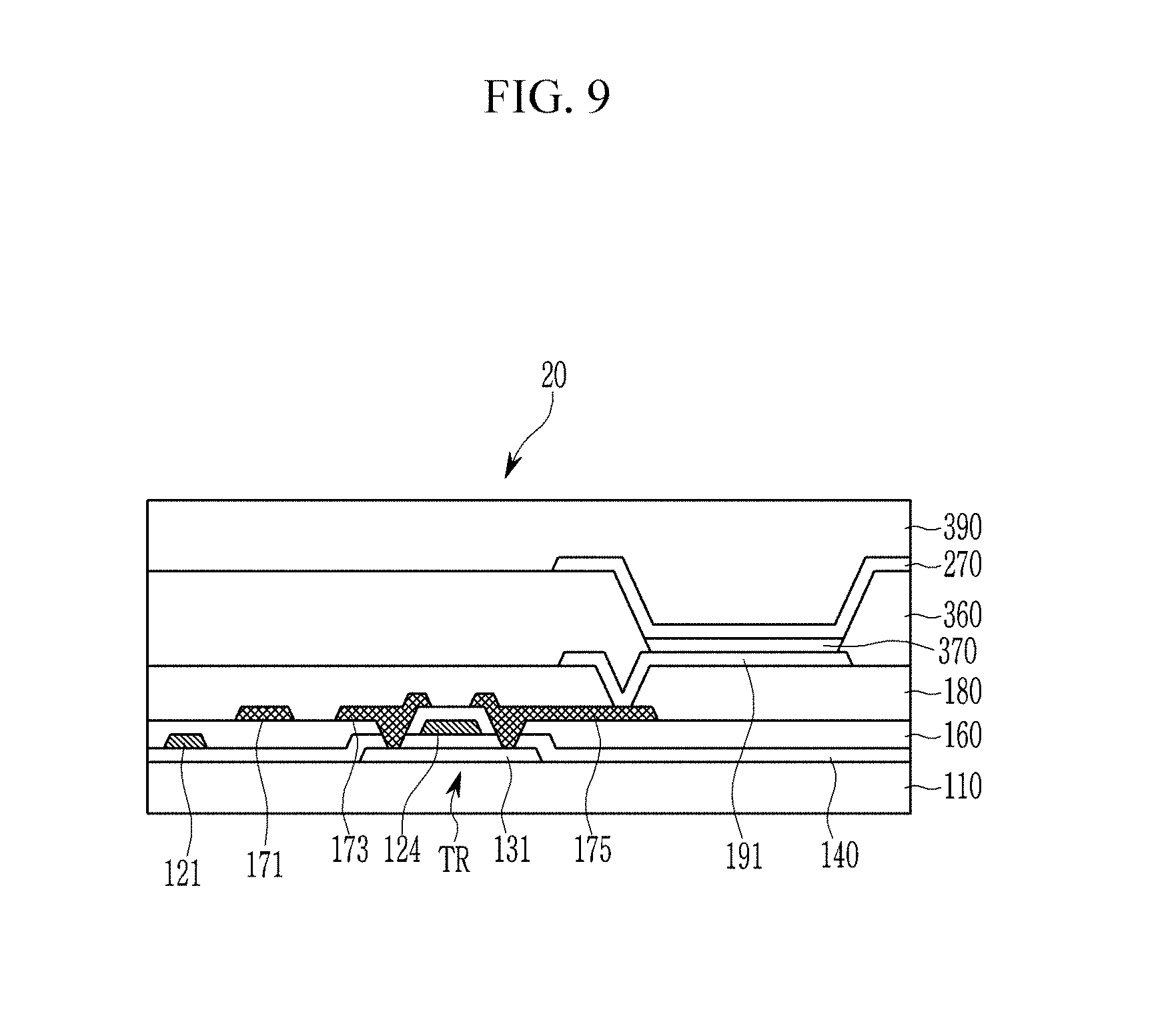
[0017] The plasma-etching of the conductive layer may include forming a data line, a source electrode, and a drain electrode.
[0018] The substrate may be a plastic substrate.
[0019] Copper may be dry-etched without additionally using energy such as heat energy, light energy, plasma energy, and the like. In addition, deposition of a by-product in an etching apparatus may be prevented during etching of copper, critical dimensions may be precisely controlled, and process stability may be improved. Further, there are several beneficial effects that may be appreciated throughout the specification.
BRIEF DESCRIPTION OF THE DRAWINGS
[0020] The above and other advantages and features of this disclosure will become more apparent by describing in further detail exemplary embodiments thereof with reference to the accompanying drawings.
[0021] FIG. 1 is a schematic diagram of a plasma etching apparatus according to an exemplary embodiment.
[0022] FIG. 2 is a flowchart of the copper plasma etching method according to an exemplary embodiment.
[0023] FIG. 3 is a schematic diagram of the copper plasma etching process according to an exemplary embodiment.
[0024] FIG. 4 is a photograph that shows etching results depending on whether or not reactive ion etching is applied.
[0025] FIG. 5 a photograph that shows etching results according to a flow rate ratio of hydrogen chloride and H.sub.2 gas.
[0026] FIG. 6 is an electron microscope photograph that shows etching results when a flow rate ratio of hydrogen chloride to H.sub.2 gas is 47.5:12.5.
[0027] FIG. 7 is a graph that shows optical emission spectroscopy (OES) intensity according to etching time.
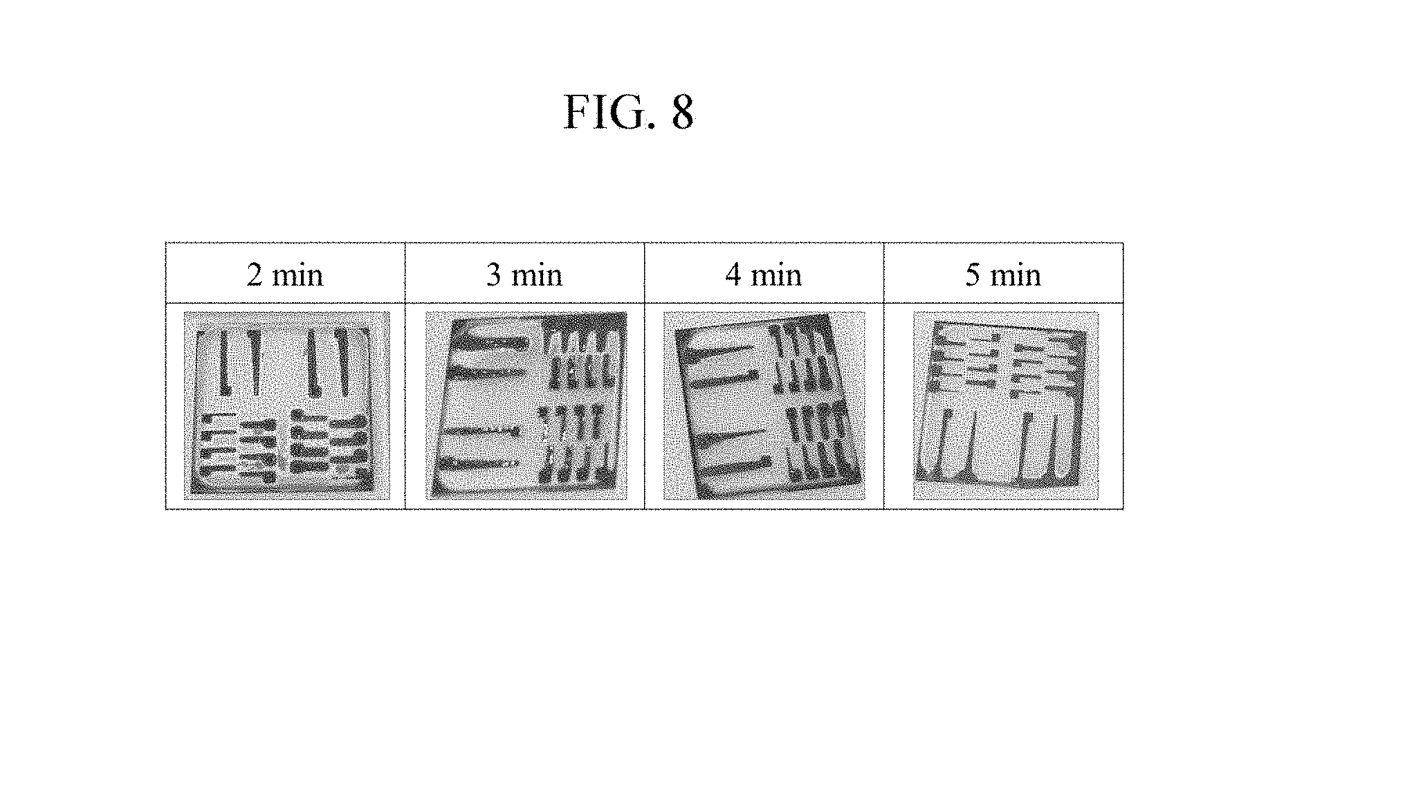
[0028] FIG. 8 is a photograph that shows etching results according to etching time.
[0029] FIG. 9 is a schematic cross-sectional view of an organic light emitting display panel according to an exemplary embodiment.
[0030] FIG. 10 is a schematic cross-sectional view of a liquid crystal display panel according to an exemplary embodiment.
DETAILED DESCRIPTION
[0031] The present invention will be described more fully hereinafter with reference to the accompanying drawings, in which exemplary embodiments of the invention are shown. As those skilled in the art would realize, the described embodiments may be modified in various different ways, all without departing from the spirit or scope of the present invention.
[0032] The drawings and description are to be regarded as illustrative in nature and not restrictive. Like reference numerals designate like elements throughout the specification.
[0033] In addition, the size and thickness of each configuration shown in the drawings are arbitrarily shown for better understanding and ease of description, but the present invention is not limited thereto. In the drawings, the thickness of layers, films, panels, regions, etc., are exaggerated for clarity. In the drawings, for better understanding and ease of description, the thickness of some layers and areas is exaggerated.
[0034] It will be understood that when an element such as a layer, film, region, or substrate is referred to as being "on" another element, it can be directly on the other element or intervening elements may also be present. In contrast, when an element is referred to as being "directly on" another element, there are no intervening elements present.
[0035] In addition, unless explicitly described to the contrary, the word "comprise" and variations such as "comprises" or "comprising" will be understood to imply the inclusion of stated elements but not the exclusion of any other elements.
[0036] Further, in this specification, unless explicitly described to the contrary, the phrase "on a plane" means viewing a target portion from the top, and the phrase "on a cross-section" means viewing a cross-section formed by vertically cutting a target portion from the side.
[0037] It will be understood that, although the terms "first," "second," "third" etc. may be used herein to describe various elements, components, regions, layers and/or sections, these elements, components, regions, layers and/or sections should not be limited by these terms. These terms are only used to distinguish one element, component, region, layer or section from another element, component, region, layer or section. Thus, "a first element," "component," "region," "layer" or "section" discussed below could be termed a second element, component, region, layer or section without departing from the teachings herein.
[0038] The terminology used herein is for the purpose of describing particular embodiments only and is not intended to be limiting. As used herein, the singular forms "a," "an," and "the" are intended to include the plural forms, including "at least one," unless the content clearly indicates otherwise. "At least one" is not to be construed as limiting "a" or "an." "Or" means "and/or." As used herein, the term "and/or" includes any and all combinations of one or more of the associated listed items.
[0039] Furthermore, relative terms, such as "lower" or "bottom" and "upper" or "top," may be used herein to describe one element's relationship to another element as illustrated in the Figures. It will be understood that relative terms are intended to encompass different orientations of the device in addition to the orientation depicted in the Figures. For example, if the device in one of the figures is turned over, elements described as being on the "lower" side of other elements would then be oriented on "upper" sides of the other elements. The exemplary term "lower," can therefore, encompasses both an orientation of "lower" and "upper," depending on the particular orientation of the figure. Similarly, if the device in one of the figures is turned over, elements described as "below" or "beneath" other elements would then be oriented "above" the other elements. The exemplary terms "below" or "beneath" can, therefore, encompass both an orientation of above and below.
[0040] "About" or "approximately" as used herein is inclusive of the stated value and means within an acceptable range of deviation for the particular value as determined by one of ordinary skill in the art, considering the measurement in question and the error associated with measurement of the particular quantity (i.e., the limitations of the measurement system). For example, "about" can mean within one or more standard deviations, or within .+-.20%, 10%, or 5% of the stated value.
[0041] Unless otherwise defined, all terms (including technical and scientific terms) used herein have the same meaning as commonly understood by one of ordinary skill in the art to which this disclosure belongs. It will be further understood that terms, such as those defined in commonly used dictionaries, should be interpreted as having a meaning that is consistent with their meaning in the context of the relevant art and the present disclosure, and will not be interpreted in an idealized or overly formal sense unless expressly so defined herein.
[0042] Exemplary embodiments are described herein with reference to cross section illustrations that are schematic illustrations of idealized embodiments. As such, variations from the shapes of the illustrations as a result, for example, of manufacturing techniques and/or tolerances, are to be expected. Thus, embodiments described herein should not be construed as limited to the particular shapes of regions as illustrated herein but are to include deviations in shapes that result, for example, from manufacturing. For example, a region illustrated or described as flat may, typically, have rough and/or nonlinear features. Moreover, sharp angles that are illustrated may be rounded. Thus, the regions illustrated in the figures are schematic in nature and their shapes are not intended to illustrate the precise shape of a region and are not intended to limit the scope of the present claims.
[0043] In dry-etching of copper (Cu), a halogen-group gas including fluorine (F) or chlorine (Cl) may be desirable, and a mixture gas containing hydrogen (H), nitrogen (N), helium (He), argon (Ar), and the like may be used as necessary. When a mixture gas containing chlorine is used, chlorine ions and radicals are formed by using plasma and then reacted with copper such that a reactant such as copper (I) chloride (CuCl) or copper (II) chloride (CuCl.sub.2) may be formed. Under typical conditions, the reactant may stay in a liquid phase or a solid phase, and therefore copper may be etched through evaporation by applying additional energy (e.g., heat energy, light energy, plasma energy, and the like).
[0044] An evaporation point of CuCl or CuCl.sub.2 is about 1000.degree. C. under normal pressure, and is about 150.degree. C. in a vacuum of about 10.sup.-2 to 10.sup.-4 Torr, which may be a typical pressure of an etching apparatus that uses a plasma source. Thus, when a thermal method is used, CuCl or CuCl.sub.2 is heated to about 200.degree. C. or higher to fully etch CuCl or CuCl.sub.2 such that no residue remains. When an optical method is used, the etching apparatus may vaporize copper by irradiating a radiation beam having energy of about 2.2 electronvolts (eV) or greater to CuCl or CuCl.sub.2 by using a UV source. However, vaporized CuCl or CuCl.sub.2 in the form of a solid may be redeposited on an interior surface of a substrate or a chamber when energy is exhausted because of contact with the interior surface of the chamber when the vaporized CuCl or CuCl.sub.2 is discharged to the outside of the chamber. When the redeposition is continued, an exhaust condition for maintaining the vacuum state may be changed, and when the redeposition is significantly increased, a pipe may become clogged and the plasma may not be maintained. In addition, etching by-products redeposited to the chamber may form particles, thereby interrupting etching. Further, the etching by-products may contaminate the substrate, thereby deteriorating quality of a product or reducing the yield.
[0045] In order to solve such problems, according to an exemplary embodiment, a process condition that effectively converts CuCl or CuCl.sub.2, which is a chlorine reactant, into CuH and Cu.sub.3Cl.sub.3, which may be vaporized at room temperature is provided. For example, a temperature of a susceptor (also referred to as a susceptor electrode or a lower electrode) on which a substrate is placed is maintained to be lower than a temperature of other constituent elements of the etching apparatus to thereby etch copper without causing the above-stated problems.
[0046] According to an exemplary embodiment, an apparatus for dry-etching copper without using an additional energy source for vaporization of an etching by-product, and a method thereof, are provided. High-density plasma is formed as an electron cyclotron resonance (ECR) plasma source, and chlorine (Cl) and hydrogen (H) are continuously supplied with the same ratio by using hydrogen chloride as etching gas such that CuH and Cu.sub.3Cl.sub.3 which are in a gas phase at room temperature are generated. Optionally, H.sub.2 gas is added to the etching gas to increase hydrogen (H) radical density to thereby increase process stability and accelerate reaction speed for generation of CuH and Cu.sub.3Cl.sub.3. A flow rate ratio (H.sub.2/HCl) of the H.sub.2 gas with respect to the hydrogen chloride may be, for example, 1 or less or 0.2 or less.
[0047] FIG. 1 is a schematic diagram of a plasma etching apparatus according to an exemplary embodiment, FIG. 2 is a flowchart of a copper plasma etching method according to an exemplary embodiment, and FIG. 3 is a schematic diagram of a copper plasma etching process according to an exemplary embodiment.
[0048] Referring to FIG. 1, a plasma etching apparatus 10 includes a process chamber 101, a microwave generator 102 that generates microwaves, and a magnetic field generator 103 that includes magnetic coils for generation of a magnetic field. In addition, the plasma etching apparatus 10 includes a susceptor 104 on which a substrate S is placed in the process chamber 101, a cooling device 106, and a radio frequency (RF) generator 107. Although not illustrated, the plasma etching apparatus 10 includes a gas injection device for injection of gas into the process chamber 101 and an exhaust device that may exhaust gas (i.e., gas generated during etching) from the process chamber 101 and control a pressure in the process chamber 101. The plasma etching apparatus 10 may include several devices for control and operation or may be connected to such devices. The exemplary plasma etching apparatus 10 may be variously modified as may be determined by a person skilled in the art.
[0049] The plasma etching apparatus 10 simultaneously uses an electric field and a magnetic field to form high-density plasma having a high plasma electron temperature, and may be called an ECR etching apparatus or an ECR plasma generator. When a microwave generated using the microwave generator 102 has a frequency that matches an electron gyrofrequency of a magnetic field generated using the magnetic field generator 103, electron cyclotron resonance occurs in the magnetic field in the process chamber 101. When gas is injected into such an ECR region, the gas is ionized such that plasma is formed and electrons in the plasma are accelerated due to the resonance while passing through the region so that high energy may be acquired, e.g., achieved, and a gas ionization rate is increased because a diffusion loss is reduced due to magnetic field so that high-density plasma having a high plasma electron temperature may be generated.
[0050] FIG. 2 shows a process for etching copper using the plasma etching apparatus 10 as shown in FIG. 1.
[0051] Referring to FIG. 1 and FIG. 2, a substrate S to be etched is prepared (510). The substrate S may be any substrate that is appropriate to be etched, for example, a silicon substrate such as a wafer, a display substrate, a solar substrate, and the like. A copper layer on which a circuit that includes a wire, an electrode, and the like or an electrode is going to be formed by being etched is formed in the substrate S, and a mask may be formed or placed on the copper layer. The mask may define a portion to be etched in the copper layer. The mask may be a hard mask formed of a silicon oxide and the like, or may be formed of a photoresist. In addition to the copper layer, one or more layers to be patterned or not to be patterned may be included in the substrate S. The at least one layer may be any layer that is appropriate for a specific device. The prepared substrate S is placed on the susceptor 104 in the process chamber 101.
[0052] After the substrate S is placed on the susceptor 104 in the process chamber 101, hydrogen chloride, or hydrogen chloride and H.sub.2 gas, are supplied into the process chamber 101 (S20). The hydrogen chloride, or the hydrogen chloride and the H.sub.2 gas, are used as a process gas or an etching gas for etching copper. Next, chlorine plasma and hydrogen plasma are formed from the process gas by using an ECR plasma source (S30). The ECR plasma source may be supplied using the microwave generator 102 and the magnetic field generator 103.
[0053] The copper layer of the substrate S is etched corresponding to patterns of the mask using the chlorine (Cl) plasma and the hydrogen (H) plasma (S40). The etching may be carried out through the following three stage reactions.
First reaction stage: Cu+Cl.fwdarw.CuCl(s)
Second reaction stage: CuCl+Cl.fwdarw.CuCl.sub.2(s)
Third reaction stage: CuCl.sub.2+3H.fwdarw.CuH(g)+2HCl(g)
3CuCl.sub.2+3H.fwdarw.Cu.sub.3Cl.sub.3(g)+3HCl(g)
3CuCl.sub.2+3/2H.sub.2.fwdarw.Cu.sub.3Cl.sub.3(g)+3HCl(g)
[0054] CuCl and CuCl.sub.2 generated in the first and second reaction stages are non-volatile materials at room temperature and are vaporized when heat of about 150.degree. C. or greater is applied at about 10.sup.-2 to 10.sup.-4 Torr, which may be a process pressure of the plasma etching apparatus 10. However, since heat is generated from generation of CuCl and CuCl.sub.2 through reaction between copper and chlorine and an internal temperature of the process chamber 101 is increased due to energy from plasma, CuCl and CuCl.sub.2 may be partially vaporized without additional heat supply. Thus, when the copper is etched, vaporization of CuCl and CuCl.sub.2 may need to be suppressed in order to redeposit CuCl and CuCl.sub.2 in the process chamber 101 when copper is etched. A temperature increase of the substrate S may be suppressed, and the temperature of the substrate S may be controlled through the susceptor 104. Since the substrate S is placed on the susceptor 104, the temperature of the substrate S may be approximately the same as or similar to a temperature Ts of the susceptor 104.
[0055] For the temperature control of the substrate S, the temperature Ts of the susceptor 104 on which the substrate S is placed may be set to be the lowest in the entire configuration of the plasma etching apparatus 10, for example, in the process chamber 101 and the configuration in the process chamber 101. During the etching process, the temperature Ts of the susceptor 104 may be maintained to be lower than an interior wall temperature Tc of the process chamber 101. The interior wall temperature Tc of the process chamber 101 may be higher than room temperature, and the temperature Ts of the susceptor 104 may be lower than room temperature. According to an exemplary embodiment, the temperature Ts of the susceptor 104 may be maintained at a temperature that is lower than the interior wall temperature Tc of the process chamber 101, for example, about 10.degree. C. or less. Although the interior wall temperature Tc of the process chamber 101 is decreased to be lower than the evaporation point of CuCl and CuCl.sub.2, for example, to about 100.degree. C., heat energy or ion bombardment in the plasma is dispersed and therefore the substrate S may be locally heated to vaporize CuCl and CuCl.sub.2 with respect to particles having high energy. When the temperature Ts of the susceptor 104 is sufficiently decreased, for example, to less than about 10.degree. C., the entire substrate S may be maintained at a temperature that is lower than the evaporation point of CuCl and CuCl.sub.2.
[0056] It may be advantageous when the temperature of the susceptor 104 is as low as possible, but if the temperature is too low, a process error may occur due to condensation in the plasma etching apparatus 10. Thus, the temperature Ts of the susceptor 104 may be higher than the temperature that causes the condensation. For example, the temperature Ts may be higher than about -50.degree. C. The temperature Ts of the susceptor 104 may be controlled using the cooling device 106 connected to the susceptor 104, and for example, the temperature Ts of the susceptor 104 may be set to a predetermined temperature by circulating a coolant to the susceptor 104.
[0057] While the temperature Ts of the susceptor 104 is maintained at a sufficiently low level of less than about 10.degree. C. (i.e., Ts<Tc), the etching reaction of the third reaction stage is performed to effectively generate CuH and Cu.sub.3Cl.sub.3.
[0058] Referring to FIG. 3, CuCl is formed through reaction of copper (Cu) and chlorine (Cl) radicals, and chlorine is continuously supplied for additional reaction of CuCl and chlorine radicals in the second reaction stage such that copper in a portion (i.e., a portion not covered with the mask M) to be etched in the copper layer is saturated with CuCl.sub.2. In the third reaction stage, CuH and Cu.sub.3Cl.sub.3, which are materials that are maintained in a gaseous state at room temperature and normal pressure from reaction of CuCl.sub.2 and hydrogen radicals and then vaporized, completely etch the copper. Hydrogen chloride (HCl) is also generated in the third reaction stage, and the hydrogen chloride is split into hydrogen radicals and chlorine radicals by a plasma source and thus is reused in a copper etching process. Cu.sub.3Cl.sub.3 is not split since it has material stability, and thus may be discharged to the outside of the process chamber 101 in a gaseous state.
[0059] In order to continuously maintain the etching reaction of the third reaction stage, hydrogen ions and radicals may be supplied in an equal or greater amount than chloride ions and radicals.
N.sub.H radical.gtoreq.N.sub.Cl radical
[0060] According to an exemplary embodiment, hydrogen chloride gas is used as the etching gas. Hydrogen chloride is split by using an ECR plasma source so that hydrogen radicals and chloride radicals may be generated with the same ratio. Additionally, H.sub.2 gas is supplied to increase the number of hydrogen radicals. When H.sub.2 radicals that are not decomposed into the hydrogen radicals react with CuCl.sub.2 and thus Cu.sub.3Cl.sub.3 is formed, heat absorption occurs so that a temperature of the substrate S that is placed on the susceptor 104 may be decreased. Thus, supply of the H.sub.2 gas may suppress vaporization of an unnecessary CuCl and CuCl.sub.2 reactant and improve process stability.
[0061] When the ECR plasma source is used in the etching process, it may be advantageous in the process because the ECR plasma source includes high-density plasma, for example, about 10.sup.11/cm.sup.3 or greater and high energy, for example, about 1 eV to about 10 eV compared to an inductively coupled plasma (ICP) source or a capacitively coupled plasma (CCP). Since H.sub.2 has a high energy bond of about 4.52 eV at room temperature, the ECR plasma source may be desirable to effectively form hydrogen radicals. As described above, the microwave generator 102 and the magnetic field generator 103 of the plasma etching apparatus 10 may be used as the ECR plasma source.
[0062] FIG. 4 is a photograph that shows etching results depending on application of reactive ion etching.
[0063] In FIG. 4, the left drawing is a photograph that shows a copper layer sample etched by using an ECR plasma source having power of 900 watts (W), and the right drawing is a photograph that shows a copper layer sample etched by applying reactive ion etching (RIE) having a -150 volts (V) self-bias, together with the ECR plasma source having power of 900 W. When the RIE mode is combined to, e.g., used on, the susceptor 104, ion reaction is added such that anisotropic etching may be improved. The reactive ion etching may be performed by, for example, applying a radio frequency to the susceptor 104 by using the RF generator 107.
[0064] FIG. 5 is a photograph that shows etching results according to a flow rate ratio of hydrogen chloride and H.sub.2 gas, and FIG. 6 is a scanning electron microscope photograph that shows etching results when the flow rate ratio of hydrogen chloride and H.sub.2 gas is 47.5:12.5.
[0065] When the number of hydrogen radicals is too large, a long time may be required for CuCl.sub.2 to reach a saturation state, and etching may be interrupted. Thus, it may be advantageous to use an appropriate ratio. In order to acquire, e.g., achieve, etching results according to a gas ratio, ECR power was set to 900 W, RIE was set to 50 W (-150 V), a gap between a plasma source and a substrate (corresponding to a gap between an opposing electrode 105 and the substrate S in FIG. 1) was set to 1 centimeter (cm), and processing time was set to 300 seconds, and the copper layer was etched while adjusting the gas ratio by adjusting a flow rate of hydrogen chloride and H.sub.2 gas. FIG. 5 shows some of the etching results.
[0066] The etching rate is decreased as the flow rate ratio of H.sub.2 gas is increased, and when the flow rate ratio of HCl:H.sub.2 becomes 40:20, the copper layer is not etched within 300 seconds, and various and effective copper etching rates and various copper micropatterns may be acquired, e.g., achieved, when the flow rate ratio (H.sub.2/HCl) of H.sub.2 with respect to hydrogen chloride is between 0 and 0.5. When the flow rate ratio (H.sub.2/HCl) exceeds 0.5, an etching time is rapidly increased, which may be caused due to an insufficient amount of chlorine radicals. When the flow rate ratio (H.sub.2/HCl) exceeds 1, a CuCl.sub.x layer is not sufficiently formed, thereby interrupting etching.
[0067] In addition, when the flow rate ratio of HCl:H.sub.2 was 47.5:12.5, copper etching critical dimensions (CD) may be precisely controlled as shown in FIG. 6. That is, when the flow rate ratio (H.sub.2/HCl) was about 0.263, a copper layer having a thickness of about 5000 angstroms (.ANG.) and a width of about 1 nanometers (nm) to about 2 nm was able to be micropatterned with a high etching rate of about 300 nanometers per minute (nm/min). Thus, when the etching rate and the etching critical dimension are considered together, it may be advantageous when the flow rate ratio (H.sub.2/HCl) is about 0.263 or less (i.e., when a flow rate ratio (HCl/H.sub.2) of HCl with respect to H.sub.2 was about 3.8 or more). In a process aspect, it may be advantageous when a total flow amount of the etching gas is increased according to a substrate size, a pattern design, and a process environment, and for example, the total flow amount may be increased to about 100 cubic centimeters per minute (sccm), and the flow rate ratio of hydrogen chloride may be changed depending on process conditions.
[0068] FIG. 7 is a graph that shows OES intensity according to an etching time, and FIG. 8 is a photograph that shows etching results according to the etching time.
[0069] The above-stated third stage etching reaction may be confirmed from optical emission spectroscopy (OES) data and copper etching results according to the etching time. As the process conditions, the ECR power was set to 900 W, RIE was set to 50 W (-150 V), a gap between the plasma source and the substrate was set to 1 cm, the flow rate ratio of HCl:H.sub.2 was set to 47.5:12.5, and the etching times were set to 120 seconds (s), 180 s, 240 s, and 300 s, and the etching results were compared. As shown in FIG. 7, from the moment that the plasma is turned on, intensity of CuCl.sub.x is increased the fastest by radical reaction of copper and chlorine such that the intensity reaches the peak value at 120 seconds. In this case, it may be observed that the growth of CuCl.sub.x reaches a saturation state and then is vaporized to CuH or Cu.sub.3Cl.sub.3 by reacting with hydrogen radicals such that the intensity of CuCl.sub.x is decreased. Through this experiment, the third stage etching reaction according to an exemplary embodiment may be verified.
[0070] According to an exemplary embodiment, the etching apparatus and the etching method that may etch copper without an additional energy source at room temperature may be provided. High-density plasma is formed by using the ECR plasma source, and HCl is used as an etching gas such that chlorine and hydrogen may be continuously supplied with the same ratio. Selectively, H.sub.2 gas is added to increase density of the hydrogen radicals to thereby increase process stability, and the process for forming the Cu.sub.3Cl.sub.3 and CuH reactant having a gaseous state at room temperature and normal pressure may be accelerated through the etching reaction of the third reaction.
[0071] Referring back to FIG. 1, the temperature Ts of the susceptor 104 on which the substrate S on which the previously described reaction occurs is placed is maintained to be significantly lower than temperatures of other constituent elements of the etching apparatus 10 (e.g., Ts<Tc) to suppress evaporation of a non-volatile etching by-product, thereby stably maintaining the process. However, unlike a typical method in which copper is etched by increasing a temperature of the substrate S, according to an exemplary embodiment, copper may be etched with precise critical dimensions while maintaining the temperature Ts of the susceptor 104 at about 10.degree. C. or less to suppress evaporation of CuCl and CuCl.sub.2. The temperature Ts of the susceptor 104 is decreased to the lowest in the entire configuration of the etching apparatus 10 such that the temperature of the substrate S may be decreased.
[0072] For the copper etching reaction of the third reaction, it may be advantageous to supply the number of hydrogen radicals to be equal to or greater than the number of chlorine radicals. Thus, the H.sub.2 gas may be added to the hydrogen chloride, which is an etching gas, and H.sub.2 and CuCl.sub.2 are chemically reacted such that heat absorption occurs. When copper is etched by forming hydrogen radicals and chlorine radicals only using hydrogen chloride gas, there may be restrictions in some cases. For example, a certain portion in the process chamber 101 may be temporarily excessively heated due to heat generated from the process of forming CuCl and CuCl.sub.2 and plasma heat. Although the temperature Ts of the susceptor 104 is maintained to be less than about 10.degree. C. in order to decrease the temperature of the substrate S, excessively high heat may be applied to the copper layer of the substrate or a mask formed on the copper layer. When the mask is a photo-resist or the substrate S is formed of plastic (e.g., an organic polymer), the mask or the substrate S may be damaged due to the momentary high heat. When H.sub.2 is supplied, H.sub.2 and CuCl.sub.2 react with each other such that Cu.sub.3Cl.sub.3 is formed while causing heat absorption, and then the internal temperature of the process chamber 101 may be decreased, thereby suppressing evaporation of CuCl and CuCl.sub.2 and releasing or removing process restrictions.
[0073] Hereinafter, a display panel that is one of various electronic devices and electronic parts on which the above-described etching method may be applied will be described. The etching methods may be used in manufacturing of a display panel such as an organic light emitting display panel, a liquid crystal display panel, and the like.
[0074] FIG. 9 is a schematic cross-sectional view of an organic light emitting display panel according to an exemplary embodiment, and FIG. 10 is a schematic cross-sectional view of a liquid crystal display panel according to an exemplary embodiment.
[0075] As will be appreciated by those of ordinary skill in the art, the display panel may include various configurations other than the configurations shown. First, an organic light emitting display panel will be described, and a liquid crystal display panel will be described with a focus on differences therefrom.
[0076] Referring to FIG. 9, a display panel 20 includes a substrate 110, and signal lines and elements that are formed of several layers on the substrate 110.
[0077] The substrate 110 may be a flexible substrate formed of a plastic (e.g., a polymer) film. For example, the substrate 110 may be formed of a polymer such as polyimide, polyamide, polyester such as polyethylene terephthalate, and the like. The substrate 110 may be a hard substrate made of glass or silicon.
[0078] The substrate 110 may include a barrier layer (not shown) that prevents dispersion of an impurity that deteriorates a semiconductor characteristic and prevents permeation of moisture and the like.
[0079] A semiconductor 131 of a transistor TR is positioned on the substrate 110, and a gate insulating layer 140 is positioned on the semiconductor 131. The semiconductor 131 includes a source region and a drain region, and a channel region that is disposed between the source region and the drain region. The semiconductor 131 may include polysilicon, an oxide semiconductor, or amorphous silicon. The gate insulating layer 140 may be formed by depositing an inorganic insulating material such as a silicon oxide, a silicon nitride, and the like.
[0080] A gate conductor that includes a gate line 121 and a gate electrode 124 of the transistor TR is positioned on the gate insulating layer 140. The gate conductor may be formed by depositing a conductive material such as copper (Cu), aluminum (Al), silver (Ag), molybdenum (Mo), chromium (Cr), tantalum (Ta), titanium (Ti), and the like on the substrate 110 and patterning the same.
[0081] When copper is used as the gate conductor, a copper layer is formed by sputtering, as an example, on the substrate 110. Next, a mask is formed or disposed on the copper layer and then etched by using the copper plasma etching method according to an above-described exemplary embodiment such that the gate conductor, which is a patterned copper layer, is formed. When the copper layer is etched, a temperature of a susceptor on which the substrate 110 is placed is maintained at about 10.degree. C. or less to thereby decrease a temperature of the substrate 110, and H.sub.2 additionally supplied to an etching gas reacts with CuCl.sub.2 while causing heat absorption so that the temperature of the substrate 110 may be decreased, and accordingly, a photoresist that may be vulnerable to heat may be used as a mask. In addition, since the substrate 110 is maintained at a low temperature, the substrate 110 is not damaged during dry-etching of the copper layer even if, for example, a plastic substrate is used.
[0082] An interlayer insulating layer 160 is positioned on the gate conductor. The interlayer insulating layer 160 may include an inorganic insulating material. A data conductor that includes a data line 171, and a source electrode 173 and a drain electrode 175 of the transistor TR, is disposed on the interlayer insulating layer 160. The source electrode 173 and the drain electrode 175 are respectively connected with the source region and the drain region of the semiconductor 131 through contact holes formed in the interlayer insulating layer 160 and the gate insulating layer 140. The data conductor may include a metal such as copper (Cu), aluminum (Al), silver (Ag), molybdenum (Mo), chromium (Cr), gold (Au), platinum (Pt), palladium (Pd), tantalum (Ta), tungsten (W), titanium (Ti), nickel (Ni), and the like, or a metal alloy. When copper is used as the data conductor, the data conductor may be formed by etching a copper layer in the same manner as in the above-described case of using copper as the gate conductor.
[0083] A planarization layer 180 may be positioned on the source electrode 173 and the drain electrode 175. The planarization layer 180 may include an organic insulating material or an inorganic insulating material.
[0084] A pixel electrode 191 is positioned on the planarization layer 180. The pixel electrode 191 is connected with the drain electrode 175 through a contact hole formed in the planarization layer 180, and receives a data signal therefrom. A portion including layers from the substrate 110 to the pixel electrode 191 may be called a transistor display panel or a thin film transistor display panel.
[0085] A pixel defining layer 360 is positioned on the planarization layer 180. The pixel defining layer 360 includes an opening that overlaps the pixel electrode 191. An emission layer 370 is positioned on the pixel electrode 191 in the opening of the pixel defining layer 360, and a common electrode 270 is positioned on the emission layer 370. The pixel electrode 191, the emission layer 370, and the common electrode 270 form an organic light emitting diode (OLED). The pixel electrode 191 may be an anode of the organic light emitting diode, and the common electrode 270 may be a cathode of the organic light emitting diode. The common electrode 270 may include a transparent conductive material such as an indium tin oxide (ITO), an indium zinc oxide (IZO), and the like. An encapsulation layer 390 that protects the organic light emitting diode is positioned on the common electrode 270.
[0086] Referring to FIG. 10 in relation to a liquid crystal display panel 30, a gate line 121 and a gate electrode 124 of a transistor TR are positioned on a substrate 110, and a gate insulating layer 140 is positioned on the gate line 121 and the gate electrode 124. A semiconductor 151 and a semiconductor 154 of the transistor TR are positioned on the gate insulating layer 140, a data line 171 is positioned on the semiconductor 151, and a source electrode 173 and a drain electrode 175 are positioned on the semiconductor 154.
[0087] When a gate conductor that includes the gate line 121 and the gate electrode 124 is formed of copper, a copper layer is formed on the substrate 110 and etched by using the copper plasma etching method according to an above-described exemplary embodiment such that the gate conductor, which is a patterned copper layer, is formed. When a data conductor that includes the data line 171, the source electrode 173, and the drain electrode 175 is formed of copper, a copper layer is formed on the substrate 110 and etched by using the copper plasma etching method according to an above-described exemplary embodiment, such that the data conductor, which is a patterned copper layer, is formed.
[0088] A planarization layer 180 is positioned on the data conductor, and a pixel electrode 191 is positioned on the planarization layer 180. The pixel electrode 191 is connected with the drain electrode 175 through a contact hole formed in the planarization layer 180, and receives a data signal therefrom. A portion including layers from the substrate 110 to the pixel electrode 191 may be called a transistor display panel or a thin film transistor display panel.
[0089] A liquid crystal layer 3 that includes liquid crystal molecules 31 is positioned on the pixel electrode 191, and an insulating layer 210 that seals the liquid crystal layer 3 together with the substrate 110 is positioned on the liquid crystal layer 3. The insulating layer 210 may be in the form of a substrate. The liquid crystal molecules 31 may be disposed apart from each other in microcavities.
[0090] A common electrode 270 is disposed below the insulating layer 210 to generate an electric field in the liquid crystal layer 3 together with the pixel electrode 191, thereby controlling an alignment direction of the liquid crystal molecules 31. An alignment layer (not shown) may be disposed between the pixel electrode 191 and the liquid crystal layer 3 and between the liquid crystal layer 3 and the common electrode 270. The common electrode 270 may be disposed between the substrate 110 and the liquid crystal layer 3.
[0091] While this invention has been described in connection with what is presently considered to be practical exemplary embodiments, it is to be understood that the invention is not limited to the disclosed embodiments, but, on the contrary, is intended to cover various modifications and equivalent arrangements included within the spirit and scope of the appended claims.
* * * * *
D00000
D00001
D00002
D00003
D00004
D00005
D00006
D00007
D00008
D00009
D00010
XML
uspto.report is an independent third-party trademark research tool that is not affiliated, endorsed, or sponsored by the United States Patent and Trademark Office (USPTO) or any other governmental organization. The information provided by uspto.report is based on publicly available data at the time of writing and is intended for informational purposes only.
While we strive to provide accurate and up-to-date information, we do not guarantee the accuracy, completeness, reliability, or suitability of the information displayed on this site. The use of this site is at your own risk. Any reliance you place on such information is therefore strictly at your own risk.
All official trademark data, including owner information, should be verified by visiting the official USPTO website at www.uspto.gov. This site is not intended to replace professional legal advice and should not be used as a substitute for consulting with a legal professional who is knowledgeable about trademark law.