Magnetic Coupling Coil Component
MATSUDA; Akihisa ; et al.
U.S. patent application number 16/141122 was filed with the patent office on 2019-04-04 for magnetic coupling coil component. The applicant listed for this patent is TAIYO YUDEN CO., LTD.. Invention is credited to Takayuki ARAI, Akihisa MATSUDA, Daisuke YAMAGUCHI.
| Application Number | 20190103216 16/141122 |
| Document ID | / |
| Family ID | 65896782 |
| Filed Date | 2019-04-04 |


View All Diagrams
| United States Patent Application | 20190103216 |
| Kind Code | A1 |
| MATSUDA; Akihisa ; et al. | April 4, 2019 |
MAGNETIC COUPLING COIL COMPONENT
Abstract
A coil component according to one embodiment of the present invention includes: a first insulator body containing first filler particles at least partially having electrical conductivity; a second insulator body containing second filler particles at least partially having electrical conductivity; a first coil conductor provided in the first insulator body and wound around a coil axis for N1 turns such that intervals between adjacent turns are g1; and a second coil conductor provided in the second insulator body and wound around the coil axis for N2 turns such that intervals between adjacent turns are g2. In the embodiment, a first coil surface of the first coil conductor faces a second coil surface of the second coil conductor, and a distance T between the first coil surface and the second coil surface satisfies a relationship T.gtoreq.g1.times.N1+g2.times.N2.
| Inventors: | MATSUDA; Akihisa; (Tokyo, JP) ; YAMAGUCHI; Daisuke; (Tokyo, JP) ; ARAI; Takayuki; (Tokyo, JP) | ||||||||||
| Applicant: |
|
||||||||||
|---|---|---|---|---|---|---|---|---|---|---|---|
| Family ID: | 65896782 | ||||||||||
| Appl. No.: | 16/141122 | ||||||||||
| Filed: | September 25, 2018 |
| Current U.S. Class: | 1/1 |
| Current CPC Class: | H01F 27/2804 20130101; H01F 17/0013 20130101; H01F 2027/2809 20130101; H01F 27/292 20130101; H01F 27/32 20130101; H01F 41/041 20130101; H01F 41/122 20130101; H01F 27/323 20130101; H01F 27/29 20130101; H01F 17/04 20130101 |
| International Class: | H01F 27/32 20060101 H01F027/32; H01F 27/28 20060101 H01F027/28; H01F 27/29 20060101 H01F027/29; H01F 41/04 20060101 H01F041/04; H01F 41/12 20060101 H01F041/12 |
Foreign Application Data
| Date | Code | Application Number |
|---|---|---|
| Sep 29, 2017 | JP | 2017-190934 |
Claims
1. A coil component, comprising: a base including a first insulator body and a second insulator body, the first insulator body containing first filler particles at least partially having electrical conductivity, the second insulator body containing second filler particles at least partially having electrical conductivity; a first coil conductor provided in the first insulator body and wound around a coil axis for N1 turns such that intervals between adjacent turns are g1; and a second coil conductor provided in the second insulator body and wound around the coil axis for N2 turns such that intervals between adjacent turns are g2, wherein a first coil surface of the first coil conductor faces a second coil surface of the second coil conductor, and a distance T between the first coil surface and the second coil surface satisfies a relationship T.gtoreq.g1.times.N1+g2.times.N2.
2. The coil component according to claim 1, wherein the first insulator body has a volume resistivity of 1.times.10.sup.7 .OMEGA.cm or lower.
3. The coil component according to claim 1, wherein the second insulator body has a volume resistivity of 1.times.10.sup.7 .OMEGA.cm or lower.
4. The coil component according to claim 1, wherein the distance T satisfies a relationship 2.times.(g1.times.N1+g2.times.N2) T.gtoreq.g1.times.N1+g2.times.N2.
5. The coil component according to claim 1, wherein the first coil conductor has a different shape than the second coil conductor.
6. The coil component according to claim 1, further comprising: a first external electrode electrically connected to one end of the first coil conductor; and a second external electrode electrically connected to another end of the first coil conductor, wherein a distance M1 between the first coil conductor and the first external electrode satisfies a relationship M1.gtoreq.g1.times.N1, and a distance M2 between the first coil conductor and the second external electrode satisfies a relationship M2.gtoreq.g1.times.N1.
7. The coil component according to claim 6, wherein the first coil conductor is connected to the first external electrode via a first via conductor, and a distance M5 between the second coil conductor and the first via conductor satisfies a relationship M5.gtoreq.g1.times.N1+g2.times.N2.
8. The coil component according to claim 6, wherein the first coil conductor is connected to the second external electrode via a second via conductor, and a distance M6 between the first coil conductor and the second via conductor satisfies a relationship M6.gtoreq.g1.times.N1.
9. The coil component according to claim 6, wherein the first coil conductor includes a first lead-out conductor and a second lead-out conductor having a different shape than the first lead-out conductor, and the first coil conductor is electrically connected to the first external electrode via the first lead-out conductor and electrically connected to the second external electrode via the second lead-out conductor.
10. The coil component according to claim 6, further comprising: a third external electrode electrically connected to one end of the second coil conductor; and a fourth external electrode electrically connected to another end of the second coil conductor, wherein a distance M3 between the second coil conductor and the third external electrode satisfies a relationship M3.gtoreq.g2.times.N2, and a distance M4 between the second coil conductor and the fourth external electrode satisfies a relationship M4.gtoreq.g2.times.N2.
11. The coil component according to claim 10, wherein the second coil conductor is connected to the third external electrode via a third via conductor, and the second coil conductor is connected to the fourth external electrode via a fourth via conductor, and a distance M7 between the second coil conductor and the fourth via conductor satisfies a relationship M7.gtoreq.g2.times.N2.
12. The coil component according to claim 6, wherein all of the first external electrode, the second external electrode, the third external electrode, and the fourth external electrode are provided on a mounting surface of the base.
13. The coil component according to claim 10, wherein the second coil conductor includes a third lead-out conductor and a fourth lead-out conductor having a different shape than the third lead-out conductor, and the second coil conductor is electrically connected to the third external electrode via the third lead-out conductor and electrically connected to the fourth external electrode via the fourth lead-out conductor.
14. The coil component according to claim 1, wherein the coil component has a thickness of 0.6 mm or smaller.
15. The coil component according to claim 1, wherein the first filler particles contain 95 wt % or more Fe.
16. The coil component according to claim 1, wherein the second filler particles contain 95 wt % or more Fe.
17. A coil component, comprising: a first insulator body containing first filler particles at least partially having electrical conductivity; a second insulator body containing second filler particles at least partially having electrical conductivity; a first coil conductor provided in the first insulator body and wound around a coil axis for N1 turns such that intervals between adjacent turns are g1; a second coil conductor provided in the second insulator body and wound around the coil axis for N2 turns such that intervals between adjacent turns are g2; a first external electrode electrically connected to one end of the first coil conductor; a second external electrode electrically connected to another end of the first coil conductor; a third external electrode electrically connected to one end of the second coil conductor; and a fourth external electrode electrically connected to another end of the second coil conductor, wherein a distance M1 between the first coil conductor and the first external electrode satisfies a relationship M1.gtoreq.g1.times.N1, a distance M2 between the first coil conductor and the second external electrode satisfies a relationship M2.gtoreq.g1.times.N1, a distance M3 between the second coil conductor and the third external electrode satisfies a relationship M3.gtoreq.g2.times.N2, and a distance M4 between the second coil conductor and the fourth external electrode satisfies a relationship M4.gtoreq.g2.times.N2.
18. A coil component, comprising: a first insulator body containing first filler particles at least partially having electrical conductivity; a second insulator body containing second filler particles at least partially having electrical conductivity; a first coil conductor provided in the first insulator body and wound around a coil axis for N1 turns such that intervals between adjacent turns are g1; a second coil conductor provided in the second insulator body and wound around the coil axis for N2 turns such that intervals between adjacent turns are g2; a first external electrode electrically connected to one end of the first coil conductor; a second external electrode electrically connected to another end of the first coil conductor; a third external electrode electrically connected to one end of the second coil conductor; a fourth external electrode electrically connected to another end of the second coil conductor; a first via conductor electrically connecting between the first coil conductor and the first external electrode; a second via conductor electrically connecting between the first coil conductor and the second external electrode; a third via conductor electrically connecting between the second coil conductor and the third external electrode; and a fourth via conductor electrically connecting between the second coil conductor and the fourth external electrode, wherein a distance M5 between the second coil conductor and the first via conductor satisfies a relationship M5.gtoreq.g1.times.N1+g2.times.N2, a distance M6 between the first coil conductor and the second via conductor satisfies a relationship M6.gtoreq.g1.times.N1, and a distance M7 between the second coil conductor and the fourth via conductor satisfies a relationship M7.gtoreq.g2.times.N2.
Description
CROSS-REFERENCE TO RELATED APPLICATIONS
[0001] This application is based on and claims the benefit of priority from Japanese Patent Application Serial No. 2017-190934(filed on Sep. 29, 2017), the contents of which are hereby incorporated by reference in their entirety.
TECHNICAL FIELD
[0002] The present disclosure relates to a magnetic coupling coil component.
BACKGROUND
[0003] A magnetic coupling coil component is an electronic component including a pair of coil units magnetically coupled to each other. Representative examples of magnetic coupling coil component include a common mode choke coil, a transformer, and a coupling inductor. Such a magnetic coupling coil component preferably has a high coupling coefficient between the pair of coil conductors.
[0004] A magnetic coupling coil component is produced by, for example, a lamination process. A magnetic coupling coil component produced by a lamination process is disclosed in Japanese Patent Application Publication No. 2016-131208. The coupling coil component disclosed in this publication includes a pair of coil units each having a coil conductor in an insulator body, and the pair of coil units are magnetically coupled to each other.
[0005] The pair of coil units are configured such that coil axes of the coil conductors of the coil units are substantially aligned with each other and the coil units are tightly contacted with each other, thereby increasing the degree of coupling between the coil conductors. The insulator body is formed by preparing a plurality of insulating sheets formed of an insulating material having an excellent insulating quality and then stacking the plurality of insulating sheets together. In many cases, the insulating material used for the insulator body is formed of ferrite.
SUMMARY
[0006] One object of the present invention is to provide a novel magnetic coupling coil component having an improved degree of coupling between the coil conductors. Other objects of the present invention will be apparent with reference to the entire description in this specification.
[0007] A coil component according to one embodiment of the present invention includes: a first insulator body containing first filler particles at least partially having electrical conductivity; a second insulator body containing second filler particles at least partially having electrical conductivity; a first coil conductor provided in the first insulator body and wound around a coil axis for N1 turns such that intervals between adjacent turns are g1; and a second coil conductor provided in the second insulator body and wound around the coil axis for N2 turns such that intervals between adjacent turns are g2. In the embodiment, a first coil surface of the first coil conductor faces a second coil surface of the second coil conductor, and a distance T between the first coil surface and the second coil surface satisfies a relationship T.gtoreq.g1.times.N1+g2.times.N2.
[0008] According to the embodiment, the first insulator body contains the first filler particles at least partially having electrical conductivity, and therefore, the first insulator body has a higher magnetic permeability than a conventional insulator body formed of ferrite and not containing electrically conductive filler particles. According to the embodiment, the second insulator body contains the second filler particles at least partially having electrical conductivity, and therefore, the second insulator body has a higher magnetic permeability than a conventional insulator body formed of ferrite and not containing electrically conductive filler particles. Accordingly, according to the above embodiment, the coil component in which the first coil conductor provided in the first insulator body and the second coil conductor provided in the second insulator body are coupled magnetically can have a higher coupling coefficient than a conventional coil component in which an insulator body does not contain electrically conductive filler particles.
[0009] In one embodiment of the present invention, the first insulator body has a volume resistivity .rho.1. The volume resistivity .rho.1 has such a value that no dielectric breakdown occurs between adjacent turns of the first coil conductor when the intervals between the adjacent turns of the first coil conductor are g1 or larger. When a voltage V1 is applied across the first coil conductor, a voltage of V1/N1 is applied between adjacent turns of the first coil conductor. The electrical resistance between adjacent turns of the first coil conductor is .rho.1.times.g1. Therefore, the first insulator body is configured such that no dielectric breakdown occurs when a voltage of V1/N1 is applied between adjacent turns of the first coil conductor. That is, the withstanding voltage of the first insulator body is V1/N1 or higher between adjacent turns of the first coil conductor (at intervals of g1). Accordingly, when a voltage V1 is applied between the first coil conductor and a conductor positioned in the first insulator body so as to be distant from the first coil conductor by g1.times.N1 or more, no dielectric breakdown occurs between this conductor and the first coil conductor in the first insulator body. In other words, insulation can be ensured between the first coil conductor and the conductor positioned in the first insulator body so as to be distant from the first coil conductor by g1.times.N1 or more.
[0010] In one embodiment of the present invention, the second insulator body has a volume resistivity .rho.2. The volume resistivity .rho.2 has such a value that no dielectric breakdown occurs between adjacent turns of the second coil conductor when the intervals between the adjacent turns of the second coil conductor are g2 or larger. When a voltage V2 is applied across the second coil conductor, a voltage of V2/N2 is applied between adjacent turns of the second coil conductor. The electrical resistance between adjacent turns of the second coil conductor is .rho.2.times.g2. Therefore, the second insulator body is configured such that no dielectric breakdown occurs when a voltage of V2/N2 is applied between adjacent turns of the second coil conductor. That is, the withstanding voltage of the second insulator body is V2/N2 or higher between adjacent turns of the second coil conductor. Accordingly, when a voltage V2 is applied between the second coil conductor and a conductor positioned in the second insulator body so as to be distant from the second coil conductor by g2.times.N2 or more, no dielectric breakdown occurs in the second insulator body. In other words, insulation can be ensured between the second coil conductor and the conductor positioned in the second insulator body so as to be distant from the second coil conductor by g2.times.N2 or more.
[0011] As described above, in the first insulator body, insulation can be ensured at a position distant from the first coil conductor by g1.times.N1 or more, and in the second insulator body, insulation can be ensured at a position distant from the second coil conductor by g2.times.N2 or more. Therefore, dielectric breakdown between the first coil surface and the second coil surface can be prevented when the distance T between the first coil surface and the second coil surface satisfies the relationship T.gtoreq.g1.times.N1+g2.times.N2.
[0012] In one embodiment of the present invention, the first insulator body has a volume resistivity of 1.times.10.sup.7 .OMEGA.cm or lower. In one embodiment of the present invention, the second insulator body has a volume resistivity of 1.times.10.sup.7 .OMEGA.cm or lower.
[0013] In one embodiment of the present invention, the distance T between the first coil surface and the second coil surface satisfies the relationship 2.times.(g1.times.N1+g2.times.N2) T.gtoreq.g1.times.N1+g2.times.N2. A large distance between the first coil surface and the second coil surface ensures the insulation but also degrades the coupling coefficient therebetween. When the upper limit of the distance T between the first coil surface and the second coil surface is 2.times.(g1.times.N1+g2.times.N2), it is possible to ensure the insulation and inhibit the coupling coefficient from being degraded.
[0014] A coil component according to one embodiment of the present invention further includes: a first external electrode electrically connected to one end of the first coil conductor; and a second external electrode electrically connected to another end of the first coil conductor, wherein a distance M1 between the first coil conductor and the first external electrode satisfies a relationship M1.gtoreq.g1.times.N1, and a distance M2 between the first coil conductor and the second external electrode satisfies a relationship M2.gtoreq.g1.times.N1.
[0015] In the embodiment, it is possible to prevent dielectric breakdown between the first coil conductor and the first external electrode to which the first coil conductor is connected.
[0016] A coil component according to one embodiment of the present invention further includes: a third external electrode electrically connected to one end of the second coil conductor; and a fourth external electrode electrically connected to another end of the second coil conductor, wherein a distance M3 between the second coil conductor and the third external electrode satisfies a relationship M3.gtoreq.g2.times.N2, and a distance M4 between the second coil conductor and the fourth external electrode satisfies a relationship M4.gtoreq.g2.times.N2.
[0017] In the embodiment, it is possible to prevent dielectric breakdown between the second coil conductor and the second external electrode to which the second coil conductor is connected.
[0018] In a coil component according to one embodiment of the present invention, the first coil conductor is connected to the first external electrode via a first via conductor, and a distance M5 between the first coil conductor and the first via conductor satisfies a relationship M5.gtoreq.g1.times.N1+g2.times.N2.
[0019] In the embodiment, it is possible to prevent dielectric breakdown between the first coil conductor and the first via conductor.
[0020] In a coil component according to one embodiment of the present invention, the first coil conductor is connected to the second external electrode via a second via conductor, and a distance M6 between the first coil conductor and the second via conductor satisfies a relationship M6.gtoreq.g1.times.N1.
[0021] In the embodiment, it is possible to prevent dielectric breakdown between the first coil conductor and the second via conductor.
[0022] In a coil component according to one embodiment of the present invention, the second coil conductor is connected to the third external electrode via a third via conductor, and the second coil conductor is connected to the fourth external electrode via a fourth via conductor, and a distance M7 between the second coil conductor and the fourth via conductor satisfies a relationship M7.gtoreq.g2.times.N2.
[0023] In the embodiment, it is possible to prevent dielectric breakdown between the second coil conductor and the fourth via conductor.
[0024] A coil component according to another embodiment of the present invention includes: a first insulator body containing first filler particles at least partially having electrical conductivity; a second insulator body containing second filler particles at least partially having electrical conductivity; a first coil conductor provided in the first insulator body and wound around a coil axis for N1 turns such that intervals between adjacent turns are g1; a second coil conductor provided in the second insulator body and wound around the coil axis for N2 turns such that intervals between adjacent turns are g2; a first external electrode electrically connected to one end of the first coil conductor; a second external electrode electrically connected to another end of the first coil conductor; a third external electrode electrically connected to one end of the second coil conductor; and a fourth external electrode electrically connected to another end of the second coil conductor. In the embodiment, a distance M1 between the first coil conductor and the first external electrode satisfies a relationship M1.gtoreq.g1.times.N1, a distance M2 between the first coil conductor and the second external electrode satisfies a relationship M2.gtoreq.g1.times.N1, a distance M3 between the second coil conductor and the third external electrode satisfies a relationship M3.gtoreq.g2.times.N2, and a distance M4 between the second coil conductor and the fourth external electrode satisfies a relationship M4.gtoreq.g2.times.N2.
[0025] In the embodiment, it is possible to prevent dielectric breakdown between the first coil conductor and the first external electrode to which the first coil conductor is connected and between the second coil conductor and the second external electrode to which the second coil conductor is connected
[0026] A coil component according to another embodiment of the present invention includes: a first insulator body containing first filler particles at least partially having electrical conductivity; a second insulator body containing second filler particles at least partially having electrical conductivity; a first coil conductor provided in the first insulator body and wound around a coil axis for N1 turns such that intervals between adjacent turns are g1; a second coil conductor provided in the second insulator body and wound around the coil axis for N2 turns such that intervals between adjacent turns are g2; a first external electrode electrically connected to one end of the first coil conductor; a second external electrode electrically connected to another end of the first coil conductor; a third external electrode electrically connected to one end of the second coil conductor; a fourth external electrode electrically connected to another end of the second coil conductor; a first via conductor electrically connecting between the first coil conductor and the first external electrode; a second via conductor electrically connecting between the first coil conductor and the second external electrode; a third via conductor electrically connecting between the second coil conductor and the third external electrode; and a fourth via conductor electrically connecting between the second coil conductor and the fourth external electrode. In the embodiment, a distance M5 between the second coil conductor and the first via conductor satisfies a relationship M5.gtoreq.g1.times.N1+g2.times.N2, a distance M6 between the first coil conductor and the second via conductor satisfies a relationship M6.gtoreq.g1.times.N1, and a distance M7 between the second coil conductor and the fourth via conductor satisfies a relationship M7.gtoreq.g2.times.N2.
[0027] In the embodiment, it is possible to prevent dielectric breakdown between the second coil conductor and the first via conductor, between the first coil conductor and the second via conductor, between the second coil conductor and the first via conductor, and between the second coil conductor and the fourth via conductor.
Advantages
[0028] According to the various embodiments of the invention disclosed herein, a magnetic coupling coil component can have an increased degree of coupling between coil conductors.
BRIEF DESCRIPTION OF THE DRAWINGS
[0029] FIG. 1 is a perspective view of a coil component according to one embodiment of the present invention.
[0030] FIG. 2 is an exploded perspective view of one of two coil units included in the coil component of FIG. 1.
[0031] FIG. 3 is an exploded perspective view of the other of the two coil units included in the coil component of FIG. 1.
[0032] FIG. 4 is a plan view of the coil component shown in FIG. 1.
[0033] FIG. 5 schematically shows a cross section of the coil component of FIG. 1 cut along the line I-I.
[0034] FIG. 6 schematically shows a cross section of the coil component of FIG. 1 cut along the line II-II.
[0035] FIG. 7 is a perspective view of a coil component according to another embodiment of the present invention.
[0036] FIG. 8 is an exploded perspective view of one of two coil units included in the coil component of FIG. 7.
[0037] FIG. 9 is an exploded perspective view of the other of the two coil units included in the coil component of FIG. 7.
[0038] FIG. 10 is a plan view of the coil component shown in FIG. 7.
[0039] FIG. 11 schematically shows a cross section of the coil component of FIG. 7 cut along the line III-III.
[0040] FIG. 12 schematically shows a cross section of the coil component of FIG. 7 cut along the line IV-IV.
DESCRIPTION OF THE EMBODIMENTS
[0041] Various embodiments of the invention will be described hereinafter with reference to the drawings. Elements common to a plurality of drawings are denoted by the same reference signs throughout the plurality of drawings. It should be noted that the drawings do not necessarily appear to an accurate scale, for convenience of description.
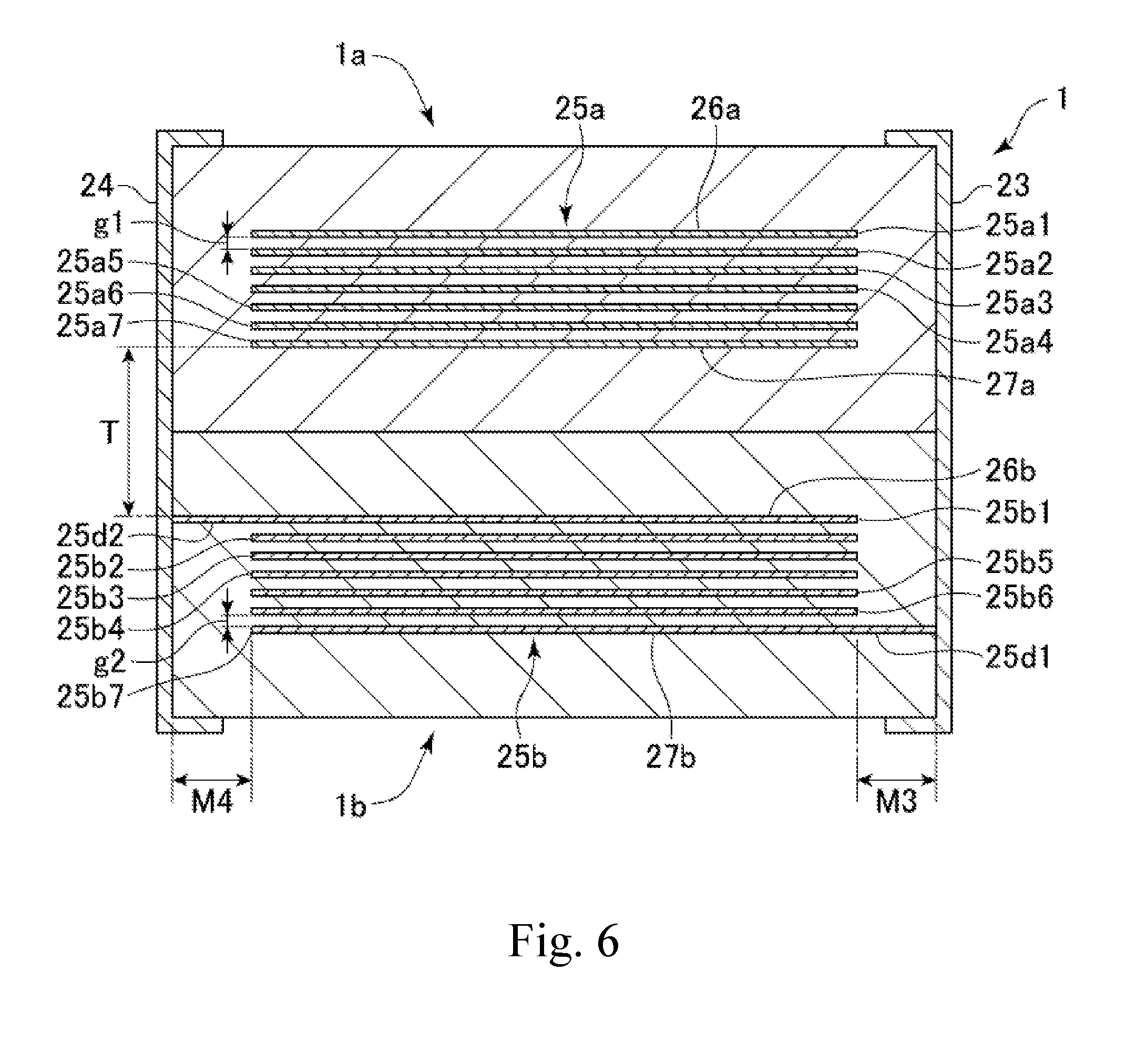
[0042] A coil component 1 according to one embodiment of the present invention will be hereinafter described with reference to FIGS. 1 to 6. FIG. 1 is a perspective view of the coil component 1 according to one embodiment of the present invention, FIG. 2 is an exploded perspective view of a coil unit 1a included in the coil component 1 of FIG. 1, FIG. 3 is an exploded perspective view of a coil unit 1b included in the coil component 1 of FIG. 1, FIG. 4 is a plan view of the coil component 1 of FIG. 1, FIG. 5 schematically shows a cross section of the coil component 1 cut along the line I-I, and FIG. 6 schematically shows a cross section of the coil component 1 cut along the line II-II. In FIG. 4, a top cover layer 18a (described later) is omitted for description of the winding pattern of the coil conductors.
[0043] These drawings show, as one example of the coil component 1, a common mode choke coil for eliminating common mode noise from a differential transmission circuit that transmits a differential signal. A common mode choke coil is one example of a magnetic coupling coil component to which the present invention is applicable. The present invention can also be applied to a transformer, a coupled inductor, and other various coil components, in addition to a common mode choke coil. A common mode choke coil is produced by, for example, a lamination process or a thin film process.
[0044] As shown, the coil component 1 according to one embodiment of the present invention includes the coil unit 1a, the coil unit 1b, an external electrode 21, an external electrode 22, an external electrode 23, and an external electrode 24.
[0045] The coil unit 1a includes an insulator body 11a, made of a magnetic material having an excellent insulating quality, and a coil conductor 25a provided in the insulator body 11a. In one embodiment, the insulator body 11a has a rectangular parallelepiped shape. One end of the coil conductor 25a is electrically connected to the external electrode 21. The other end of the coil conductor 25a is electrically connected to the external electrode 22.
[0046] The coil unit 1b may be configured in the same manner as the coil unit 1a. In the embodiment shown, the coil unit 1b includes an insulator body 11b, made of a magnetic material, and a coil conductor 25b provided in the insulator body 11b. In one embodiment, the insulator body 11b has a rectangular parallelepiped shape. One end of the coil conductor 25b is electrically connected to the external electrode 23. The other end of the coil conductor 25b is electrically connected to the external electrode 24. The coil conductor 25a and the coil conductor 25b may have the same shape or may have different shapes. In the embodiment shown, the shape of the coil conductor 25a is different from that of the coil conductor 25b. When the coil conductor 25a and the coil conductor 25b have different shapes, the inductance of the coil conductor 25a may be different from that of the coil conductor 25b.
[0047] The bottom surface of the insulator body 11a is joined to the top surface of the insulator body 11b. An insulator body 10 includes the insulator body 11a and the insulator body 11b joined to the insulator body 11a.
[0048] The insulator body 10 (also referred to as "the base 10" or "the insulating base 10") has a first principal surface 10a, a second principal surface 10b, a first end surface 10c, a second end surface 10d, a first side surface 10e, and a second side surface 10f. The outer surface of the insulator body 10 is defined by these six surfaces. The first principal surface 10a and the second principal surface 10b are opposed to each other, the first end surface 10c and the second end surface 10d are opposed to each other, and the first side surface 10e and the second side surface 10f are opposed to each other.
[0049] In FIG. 1, the first principal surface 10a lies on the top side of the insulator body 10, and therefore, the first principal surface 10a may be herein referred to as "the top surface." Similarly, the second principal surface 10b may be referred to as "the bottom surface." The coil component 1 is disposed such that the second principal surface 10b faces a circuit board (not shown), and therefore, the second principal surface 10b may be herein referred to as "the mounting surface." Furthermore, the top-bottom direction of the coil component 1 is based on the top-bottom direction in FIG. 1.
[0050] In this specification, the "length" direction, the "width" direction, and the "thickness" direction of the coil component 1 refer to the "L" direction, the "W" direction, and the "T" direction in FIG. 1, respectively, unless otherwise construed from the context.
[0051] In one embodiment of the present invention, the coil component 1 has a length (the dimension in the direction of the axis L) of 0.2 to 6.0 mm, a width (the dimension in the direction of the axis W) of 0.1 to 4.5 mm, and a thickness (the dimension in the direction of the axis T) of 0.1 to 4.0 mm. These dimensions are mere examples, and the coil component 1 to which the present invention can be applied can have any dimensions that conform to the purport of the present invention. In one embodiment, the coil component 1 has a low profile. For example, the coil component 1 has a thickness of 0.60 mm or smaller. It is also possible that the coil component 1 has a thickness of 0.55 mm or smaller. For example, the coil component 1 has a width larger than the thickness thereof.
[0052] In the embodiment shown, the external electrode 21 and the external electrode 23 are provided on the first end surface 10c of the insulator body 10. The external electrode 22 and the external electrode 24 are provided on the second end surface 10d of the insulator body 10. Each of the external electrodes are formed and arranged such that a part thereof extends along the first principal surface 10a of the insulator body 10. Each of the external electrodes are formed and arranged such that a part thereof extends along the second principal surface 10b of the insulator body 10. Each of the external electrode 21 and the external electrode 22 may be formed and arranged such that a part thereof extends along the second side surface 10f of the insulator body 10. Each of the external electrode 23 and the external electrode 24 may be formed and arranged such that a part thereof extends along the first side surface 10e of the insulator body 10.
[0053] The shapes and the arrangements of the external electrodes described explicitly in this specification are mere examples. Therefore, the shapes and the arrangements of the external electrodes that are applicable to the present invention are not limited to those explicitly described in this specification.
[0054] As shown in FIG. 2, the insulator body 11a includes a coil layer 20a, a top cover layer 18a provided on the top surface of the coil layer 20a, and a bottom cover layer 19a provided on the bottom surface of the coil layer 20a.
[0055] The coil layer 20a includes insulating layers 20a1 to 20a7 stacked together. The insulator body 11a includes an insulating layer 20a7, an insulating layer 20a6, an insulating layer 20a5, an insulating layer 20a4, an insulating layer 20a3, an insulating layer 20a2, and an insulating layer 20a1 that are stacked in this order from the negative side to the positive side in the direction of the axis T.
[0056] As will be described later, the insulating layers 20a1 to 20a7 have conductive patterns 25a1 to 25a7 formed thereon, respectively. These conductive patterns 25a1 to 25a7 and lead-out conductors 25c1, 25c2 constitute the coil conductor 25a. All the conductive patterns 25a1 to 25a7 are wound around a coil axis A. In the embodiment shown, the coil axis A extends in the direction of the axis T. This extension direction of the coil axis A is the same as the lamination direction of the insulating layers 20a1 to 20a7.
[0057] The coil conductor 25a has a top surface 26a and a bottom surface 27a. The top surface 26a is a plain surface extending through the top surface of the conductive pattern 25a1. The bottom surface 27a is a plain surface extending through the bottom surface of the conductive pattern 25a7.
[0058] In another embodiment of the present invention, the insulating layers 20a1 to 20a7 may be stacked together in the direction of the axis L. In this arrangement, the conductive patterns 25a1 to 25a7 and the lead-out conductors 25c1, 25c2 are formed on the surfaces of the insulating layers 20a1 to 20a7, and thus the coil axis A extends in the direction of the axis L, the same as the lamination direction of the insulating layers 20a1 to 20a7. In still another embodiment of the present invention, the insulating layers 20a1 to 20a7 may be stacked together in the direction of the axis W. In this arrangement, the conductive patterns 25a1 to 25a7 and the lead-out conductors 25c1, 25c2 are formed on the surfaces of the insulating layers 20a1 to 20a7, and thus the coil axis A extends in the direction of the axis W, the same as the lamination direction of the insulating layers 20a1 to 20a7.
[0059] The conductive pattern 25a1 is wound around the coil axis A for a three-fourth turn. Each of the conductive patterns 25a2 to 25a6 is wound around the coil axis A for a seven-eighth turn. The conductive pattern 25a7 is wound around the coil axis A for a one-fourth turn. The conductive pattern 25a1 is wound for a smaller number of turns than the conductive patterns 25a2 to 25a6 because it is connected with the external electrode 22. The conductive pattern 25a7 is wound for a smaller number of turns than the conductive patterns 25a2 to 25a6 because it is connected with the external electrode 21. The numbers of turns of the conductive patterns 25a1 to 25a7 are not limited to those described herein as examples. In the embodiment shown, the coil conductor 25a is wound around the coil axis A for 5.375 (=3/4+5.times.7/8+1/4) turns. The number of turns of the coil conductor 25a is not limited to that described herein as an example. The coil conductor 25a is wound around the coil axis A for N1 turns (N1 is a real number equal to or greater than two).
[0060] The top cover layer 18a is a laminate including a plurality of insulating layers stacked together. Similarly, the bottom cover layer 19a is a laminate including a plurality of insulating layers stacked together.
[0061] The coil layer 20a may include any number of insulating layers as necessary, in addition to the insulating layers 20a1 to 20a7. A part of the insulating layers 20a1 to 20a7 may be omitted as necessary.
[0062] The top cover layer 18a, the bottom cover layer 19a, and the insulating layers included in the coil layer 20a are formed of a resin material having an excellent insulating quality. Examples of the resin material include a polyvinyl butyral (PVB) resin, an ethyl cellulose resin, a polyvinyl alcohol resin, and an acrylic resin. The resin contained in the top cover layer 18a, the bottom cover layer 19a, and the coil layer 20a may be a thermosetting resin having an excellent insulating quality. Examples of the thermosetting resin include an epoxy resin, a polyimide resin, a polystyrene (PS) resin, a high-density polyethylene (HDPE) resin, a polyoxymethylene (POM) resin, a polycarbonate (PC) resin, a polyvinylidene fluoride (PVDF) resin, a phenolic resin, a polytetrafluoroethylene (PTFE) resin, or a polybenzoxazole (PBO) resin. The resin contained in one insulating layer is either the same as or different from the resin contained in another insulating layer.
[0063] In one embodiment of the present invention, at least a part of the insulating layers constituting the top cover layer 18a, the bottom cover layer 19a, and the coil layer 20a contains a large number of filler particles 29a at least partially having electrical conductivity. A part of the insulating layers constituting the top cover layer 18a, the bottom cover layer 19a, and the coil layer 20a may not contain the filler particles 29a.
[0064] The filler particles 29a are formed of various known electrically conductive materials. For example, the filler particles 29a are soft magnetic metal particles. Soft magnetic metal particles applicable to the insulating layers are made of a material in which magnetism is developed in an unoxidized metal portion, and such particles are, for example, particles including unoxidized metal particles or alloy particles. At least a part of the filler particles 29a has electrical conductivity. A part of the filler particles 29a may be insulating. For example, the filler particles 29a may have an insulating film formed on the surface thereof. The insulating film may be, for example, an oxidized film made of an oxidized soft magnetic metal material. Examples of soft magnetic metal particles applicable to the insulating layers include Fe particles made of Fe and inevitable impurities, alloy-based particles such as Fe--Si--Cr particles, Fe--Si--Al particles, and Fe--Ni particles, amorphous alloy particles such as Fe--Si--Cr--B--C particles and Fe--Si--B--Cr particles, and a mixture thereof. Powder compacts made of these particles can also be used as the filler particles 29a. These particles or powder compacts having the surface thereof thermally treated to form an oxidized film can also be used as the filler particles 29a. In one embodiment, the filler particles 29a contain 95 wt % or more Fe. Thus, occurrence of magnetic saturation in the insulator body 11a can be inhibited, and as a result, the coil component 1 can have improved direct current (DC) superposition characteristics.
[0065] The filler particles 29a are produced by the atomization method, for example. The filler particles contained in the insulating layers can also be produced by any known method other than the atomizing method. Commercially available soft magnetic metal particles can be used as the filler particles contained in the insulating layers. Examples of commercially available soft magnetic metal particles include PF-20F from Epson Atmix Corporation and SFR-FeSiAl from Nippon Atomized Metal Powders Corporation.
[0066] The filler particles 29a contained in the top cover layer 18a, the bottom cover layer 19a, and/or the coil layer 20a may have, for example, a spherical, flat, or foil-like shape. The filler particles 29a may have any shape.
[0067] The materials and the shapes of the filler particles 29a described explicitly in this specification are mere examples. Therefore, the materials and the arrangements of the filler particles 29a that are applicable to the present invention are not limited to those explicitly described in this specification.
[0068] The insulator body 11a has a volume resistivity .rho.1. In one embodiment, the insulator body 11a has a volume resistivity .rho.1 at any part in the interior thereof. It is also possible that the insulator body 11a has a uniform volume resistivity. The volume resistivity .rho.1 of the insulator body 11a has such a value that no dielectric breakdown occurs between adjacent turns of the coil conductor 25a. For example, the volume resistivity .rho.1 of the insulator body 11a is 1.times.10.sup.7 .OMEGA.cm or lower. In one embodiment of the present invention, at least a part of the top cover layer 18a, the bottom cover layer 19a, and the coil layer 20a has a volume resistivity of 1.times.10.sup.7 .OMEGA.cm or lower.
[0069] On the top surfaces of the insulating layers 20a1 to 20a7, there are provided conductive patterns 25a1 to 25a7, respectively. The conductive patterns 25a1 to 25a7 are formed by applying a conductive paste made of a metal or alloy having an excellent electrical conductivity by a printing method such as screen printing or any other known method such as plating, etching, etc. The conductive paste may be made of Ag, Pd, Cu, Al, or alloys thereof. The conductive patterns 25a1 to 25a7 may be formed by other methods using other materials.
[0070] The insulating layers 20a1 to 20a6 are provided with vias Va1 to Va6, respectively, at predetermined positions therein. The vias Va1 to Va6 are formed by drilling through-holes at predetermined positions in the insulating layers 20a1 to 20a6 so as to extend through the insulating layers 20a1 to 20a6 in the direction of the axis T and filling the conductive paste into the through-holes.
[0071] Each of the conductive patterns 25a1 to 25a7 is electrically connected to adjacent ones via the vias Va1 to Va6. For example, the conductive pattern 25a1 is electrically connected to the conductive pattern 25a2, adjacent to the conductive pattern 25a1, via the via Va1. The conductive patterns 25a1 to 25a7 connected in this manner constitute a coil conductor 25a having a spiral shape. The coil conductor 25a includes the conductive patterns 25a1 to 25a7 and the vias Va1 to Va6.
[0072] The end of the conductive pattern 25a1 opposite to the other end connected to the via Va1 is connected to the external electrode 22 via the lead-out conductor 25c2. The end of the conductive pattern 25a7 opposite to the other end connected to the via Va6 is connected to the external electrode 21 via the lead-out conductor 25c1. The lead-out conductor 25c1 is formed on the top surface of the insulating layer 20a7. The lead-out conductor 25c2 is formed on the top surface of the insulating layer 20a1. The lead-out conductor 25c1 and the lead-out conductor 25c2 may be formed of the same electrically conductive material as the conductive patterns 25a1 to 25a7.
[0073] Next, the coil unit 1b will be described. The coil unit 1b is shown in most detail in FIG. 3. As described above, the coil unit 1b may be configured in the same manner as the coil unit 1a.
[0074] The insulator body 11b includes a coil layer 20b, a top cover layer 18b provided on the top surface of the coil layer 20b, and a bottom cover layer 19b provided on the bottom surface of the coil layer 20b. The coil layer 20b is configured in the same manner as the coil layer 20a. More specifically, the coil layer 20b includes insulating layers 20b1 to 20b7 stacked together. The insulating layers 20b1 to 20b7 are configured in the same manner as the insulting layers 20a1 to 20a7.
[0075] The bottom cover layer 19b is configured in the same manner as the top cover layer 18a. More specifically, the bottom cover layer 19b is a laminate including a plurality of insulating layers stacked together. The top cover layer 18b is configured in the same manner as the bottom cover layer 19a. More specifically, the top cover layer 18b is a laminate including a plurality of insulating layers stacked together.
[0076] The insulating layers constituting the top cover layer 18b, the bottom cover layer 19b, and the coil layer 20b are formed of a resin material having an excellent insulating quality, as are the insulating layers constituting the top cover layer 18a, the bottom cover layer 19a, and the coil layer 20a. At least a part of the insulating layers constituting the top cover layer 18b, the bottom cover layer 19b, and the coil layer 20b contains a large number of filler particles 29b at least partially having electrical conductivity. The filler particles 29b are disposed in the insulating layers in the same manner as the filler particles 29a. The description on the filler particles 29a also applies to the filler particles 29b. That is, at least a part of the filler particles 29b has electrical conductivity. A part of the filler particles 29b may be insulating.
[0077] The insulator body 11b has a volume resistivity .rho.2. In one embodiment, the insulator body 11b has a volume resistivity .rho.2 at any part in the interior thereof. It is also possible that the insulator body 11b has a uniform volume resistivity. The volume resistivity .rho.2 of the insulator body 11b has such a value that no dielectric breakdown occurs between adjacent turns of the coil conductor 25b. The volume resistivity .rho.2 of the insulator body 11b is either the same as or different from the volume resistivity .rho.1 of the insulator body 11a. For example, the volume resistivity .rho.2 of the insulator body 11b is 1.times.10.sup.7 .OMEGA.cm or lower. In one embodiment of the present invention, at least a part of the top cover layer 18b, the bottom cover layer 19b, and the coil layer 20b has a volume resistivity of 1.times.10.sup.7 .OMEGA.cm or lower.
[0078] In the embodiment shown, the coil conductor 25b includes conductive patterns 25b1 to 25b7. Each of the conductive patterns 25b1 to 25b7 is formed on the top surface of the corresponding one of the insulating layers 20b1 to 20b7. Each of the conductive patterns 25b1 to 25b7 is electrically connected to adjacent ones via the vias Vb1 to Vb6. For example, the conductive pattern 25b1 is connected to the conductive pattern 25b2 via the via Vb1. The end of the conductive pattern 25b1 opposite to the other end connected to the via Vb1 is connected to the external electrode 24 via the lead-out conductor 25d2. The end of the conductive pattern 25b7 opposite to the other end connected to the via Vb6 is connected to the external electrode 23 via the lead-out conductor 25d1. The lead-out conductor 25d1 is formed on the top surface of the insulating layer 20b7. The lead-out conductor 25d2 is formed on the top surface of the insulating layer 20b1. The lead-out conductor 25d1 and the lead-out conductor 25d2 may be formed of the same electrically conductive material as the conductive patterns 25b1 to 25b7.
[0079] These conductive patterns 25b1 to 25b7 constitute the coil conductor 25b. All the conductive patterns 25b1 to 25b7 are wound around a coil axis A. The extension direction of the coil axis A is the same as the lamination direction of the insulating layers 20b1 to 20b7.
[0080] The coil conductor 25b has a top surface 26b and a bottom surface 27b. The top surface 26b is a plain surface extending through the top surface of the conductive pattern 25b1. The bottom surface 27b is a plain surface extending through the bottom surface of the conductive pattern 25b7.
[0081] Each of the conductive patterns 25b1 to 25b6 is wound around the coil axis A for a seven-eighth turn. The conductive pattern 25b7 is wound for a smaller number of turns than the other conductive patterns because it is connected with the external electrode 23. The numbers of turns of the conductive patterns 25b1 to 25b7 are not limited to those described herein as examples. In the embodiment shown, the conductive pattern 25b7 is wound around the coil axis A for a half turn. Therefore, in the embodiment shown, the coil conductor 25b is wound around the coil axis A for 5.75 (=6.times.7/8+0.5) turns. The number of turns of the coil conductor 25b is not limited to that described herein as an example. The coil conductor 25b is wound around the coil axis A for N2 turns (N2 is a real number equal to or greater than two).
[0082] Each of the constituents of the coil unit 1b is formed of the same material by the same method as the corresponding one of the constituents of the coil unit 1a. Therefore, those skilled in the art can grasp the materials and the production methods of the constituents of the coil unit 1b by referring to the description related to the constituents of the coil unit 1a.
[0083] The coil unit 1a is joined to the coil unit 1b. In one embodiment of the present invention, the coil unit 1a is disposed such that the bottom surface thereof is in contact with the top surface of the coil unit 1b. Therefore, in the embodiment shown, the bottom surface 27a of the coil conductor 25a faces the top surface 26b of the coil conductor 25b. The coil unit 1a may be disposed on the coil unit 1b such that the bottom cover layer 19a thereof is in contact with the top cover layer 18b of the coil unit 1b. The coil unit 1a may be disposed on the coil unit 1b such that the coil axis of the coil conductor 25a is aligned with the coil axis of the coil conductor 25b. In the embodiment shown, the coil axis A of the coil conductor 25a is aligned with the coil axis of the coil conductor 25b.
[0084] The coil component 1 includes a first coil (the coil conductor 25a) and a second coil (the coil conductor 25b), the first coil positioned between the external electrode 21 and the external electrode 22, the second coil positioned between the external electrode 23 and the external electrode 24. These two coils are connected to, for example, two signal lines in a differential transmission circuit, respectively. Thus, the coil component 1 can operate as a common mode choke coil.
[0085] The coil component 1 may include a third coil (not shown), in addition to the coil conductor 25a and the coil conductor 25b. The coil component 1 having the third coil additionally includes another coil unit configured in the same manner as the coil unit 1a. As with the coil unit 1a and the coil unit 1b, the additional coil unit includes a coil conductor that is connected to additional external electrodes. The coil component including three coils is used as, for example, a common mode choke coil for a differential transmission circuit having three signal lines.
[0086] In the coil component 1, the insulator body 11a contains filler particles 29a at least partially having electrical conductivity, and therefore, the insulator body 11a has a higher magnetic permeability than a conventional insulator body formed of ferrite. Likewise, the insulator body 11b contains filler particles 29b at least partially having electrical conductivity, and therefore, the insulator body 11b has a higher magnetic permeability than a conventional insulator body formed of ferrite. The increased magnetic permeability increases the coupling coefficient between the coil conductor 25a in the insulator body 11a and the coil conductor 25b in the insulator body 11b.
[0087] Next, a description is given of an example of a production method of the coil component 1. The coil component 1 can be produced by, for example, a lamination process. The first step is to produce the insulating layers 20a1 to 20a7, the insulating layers constituting the top cover layer 18a, and the insulating layers constituting the bottom cover layer 19a.
[0088] These insulating layers are produced through the following steps for example. First, filler particles at least a part of which has electrical conductivity are dispersed in a thermosetting resin (e.g., an epoxy resin), and the thermosetting resin is mixed with a solvent to produce a slurry. The slurry is applied to a surface of a base film made of a plastic and then dried, and the dried slurry is cut to a predetermined size to produce magnetic sheets to be used as the insulating layers 20a1 to 20a7, the insulating layers constituting the top cover layer 18a, and the insulating layers constituting the bottom cover layer 19a.
[0089] Next, through-holes are formed at predetermined positions in the magnetic sheets to be used as the insulating layers 20a1 to 20a7, so as to extend through the magnetic sheets in the direction of the axis T.
[0090] Next, each of the magnetic sheets is provided with a conductive pattern and a via. For example, a conductive paste made of a metal material (e.g. Ag) is applied by screen printing to the top surfaces of the magnetic sheets to be used as the insulating layers 20a1 to 20a7, thereby to form the conductive patterns 25a1 to 25a7 and the lead-out conductors 25c1, 25c2, and the metal paste is filled into the through-holes formed in the magnetic sheets to from the vias Va1 to Va6.
[0091] Next, the magnetic sheets to be used as the insulating layers 20a1 to 20a7 are stacked together to form a coil laminate to be used as the coil layer 20a. The magnetic sheets to be used as the insulating layers 20a1 to 20a7 are stacked together such that the conductive patterns 25a1 to 25a7 formed on the magnetic sheets are each electrically connected to adjacent conductive patterns through the vias Va1 to Va6.
[0092] Next, the magnetic sheets for forming the top cover layer 18a are stacked together to form a top cover layer laminate that corresponds to the top cover layer 18a, and the magnetic sheets for forming the bottom cover layer 19a are stacked together to form a bottom cover layer laminate that corresponds to the bottom cover layer 19a.
[0093] The same steps as above are performed to form a coil laminate to be used as the coil layer 20b, a top cover layer laminate corresponding to the top cover layer 18b, and the bottom cover layer laminate corresponding to the bottom cover layer 19b.
[0094] Next, the bottom cover layer laminate to be used as the bottom cover layer 19b, the coil laminate to be used as the coil layer 20b, the top cover layer laminate to be used as the top cover layer 18b, the bottom cover layer laminate to be used as the bottom cover layer 19a, the coil laminate to be used as the coil layer 20a, and the top cover layer laminate to be used as the top cover layer 18a are stacked together in this order and bonded together by thermal compression using a pressing machine to obtain a preliminary laminate.
[0095] Next, the preliminary laminate is segmented to a desired size by using a cutter such as a dicing machine or a laser processing machine to obtain a chip laminate corresponding to the insulator body 11a. Next, the chip laminate is degreased and then heated.
[0096] Next, a conductive paste is applied to both end portions of the heated chip laminate to form the external electrode 21, the external electrode 22, the external electrode 23, and the external electrode 24. Thus, the coil component 1 is obtained
[0097] Since the insulator body 11a contains the filler particles 29a at least partially having electrical conductivity, it is necessary to ensure the insulation between the coil conductor 25a and other conductors, that is, the coil conductor 25b and the external electrodes 21 to 24. Likewise, since the insulator body 11b contains the filler particles 29b at least partially having electrical conductivity, it is necessary to ensure the insulation between the coil conductor 25b and other conductors, that is, the coil conductor 25a and the external electrodes 21 to 24. The coil conductor 25a and the coil conductor 25b are configured and arranged so as to ensure insulation from other conductors. A further description will be given of the configuration and arrangement of the coil conductor 25a and the coil conductor 25b for ensuring the insulation, with reference to FIGS. 5 and 6.
[0098] As shown in these drawings, the coil conductor 25a is formed such that the intervals between adjacent turns are g1. In the embodiment shown, the interval between the bottom surface of the conductive pattern 25a1 and the top surface of the conductive pattern 25a2 corresponds to the interval between the conductive pattern in the first turn and the conductive pattern in the second turn, both numbered from the external electrode 22. Therefore, the interval between the bottom surface of the conductive pattern 25a1 and the top surface of the conductive pattern 25a2 is g1. In one embodiment, all of the interval between the bottom surface of the conductive pattern 25a2 and the top surface of the conductive pattern 25a3, the interval between the bottom surface of the conductive pattern 25a3 and the top surface of the conductive pattern 25a4, the interval between the bottom surface of the conductive pattern 25a4 and the top surface of the conductive pattern 25a5, the interval between the bottom surface of the conductive pattern 25a5 and the top surface of the conductive pattern 25a6, and the interval between the bottom surface of the conductive pattern 25a6 and the top surface of the conductive pattern 25a7 are g1.
[0099] Likewise, in the embodiment shown, the coil conductor 25b is formed such that the intervals between adjacent turns are g2. In the embodiment shown, the interval between the bottom surface of the conductive pattern 25b1 and the top surface of the conductive pattern 25b2 corresponds to the interval between the conductive pattern in the first turn and the conductive pattern in the second turn, both numbered from the external electrode 24. Therefore, the interval between the bottom surface of the conductive pattern 25b1 and the top surface of the conductive pattern 25b2 is g2. In one embodiment, all of the interval between the bottom surface of the conductive pattern 25b2 and the top surface of the conductive pattern 25b3, the interval between the bottom surface of the conductive pattern 25b3 and the top surface of the conductive pattern 25b4, the interval between the bottom surface of the conductive pattern 25b4 and the top surface of the conductive pattern 25b5, the interval between the bottom surface of the conductive pattern 25b5 and the top surface of the conductive pattern 25b6, and the interval between the bottom surface of the conductive pattern 25b6 and the top surface of the conductive pattern 25b7 are g2. The value of g2 is either the same as or different from the value of g1.
[0100] As described above, the insulator body 11a has a volume resistivity .rho.1, and the coil conductor 25a contained in the insulator body 11a is wound around the coil axis A for N1 turns. As described above, the volume resistivity .rho.1 has such a value that no dielectric breakdown occurs between adjacent turns of the coil conductor 25a. In the above embodiment, the intervals between adjacent turns of the coil conductor 25a are g1, and therefore, when a conductor in the insulator body 11a is distant from the coil conductor 25a by g1 or more, no dielectric breakdown occurs between this conductor and the coil conductor 25a during use of the coil component 1. When a voltage V1 is applied across the coil conductor 25a, a voltage of V1/N1 is applied between adjacent turns of the coil conductor 25a. Therefore, the insulator body 11a is configured such that no dielectric breakdown occurs when a voltage of V1/N1 is applied between adjacent turns of the coil conductor 25a. That is, the withstanding voltage for an interval of g1 in the insulator body 11a is V1/N1 or higher. Accordingly, when a conductor is disposed in the insulator body 11a at a position distant from the coil conductor 25a by g1.times.N1 or more, no dielectric breakdown occurs between this conductor and the coil conductor 25a even if the potential difference between this conductor and the coil conductor 25a is V1. In other words, in the insulator body 11a, insulation is ensured between the coil conductor 25a and a conductor disposed so as to be distant from the coil conductor 25a by g1.times.N1 or more.
[0101] As described above, the insulator body 11b has a volume resistivity .rho.2, and the coil conductor 25b contained in the insulator body 11b is wound around the coil axis A for N2 turns. As described above, the volume resistivity .rho.2 has such a value that no dielectric breakdown occurs between adjacent turns of the coil conductor 25b. In the above embodiment, the intervals between adjacent turns of the coil conductor 25b are g2, and therefore, when a conductor in the insulator body 11b is distant from the coil conductor 25b by g2 or more, no dielectric breakdown occurs between this conductor and the coil conductor 25b during use of the coil component 1. When a voltage V2 is applied across the coil conductor 25b, a voltage of V2/N2 is applied between adjacent turns of the coil conductor 25b. Therefore, the insulator body 11b is configured such that no dielectric breakdown occurs when a voltage of V2/N2 is applied between adjacent turns of the coil conductor 25b. That is, the withstanding voltage for an interval of g2 in the insulator body 11b is V2/N2 or higher. Accordingly, when a conductor is disposed in the insulator body 11b at a position distant from the coil conductor 25b by g2.times.N2 or more, no dielectric breakdown occurs between this conductor and the coil conductor 25b even if the potential difference between this conductor and the coil conductor 25b is V2. In other words, in the insulator body 11b, insulation is ensured between the coil conductor 25b and a conductor disposed so as to be distant from the coil conductor 25b by g2.times.N2 or more.
[0102] As described above, in the insulator body 11a, insulation is ensured between the coil conductor 25a and a conductor disposed so as to be distant from the coil conductor 25a by g1.times.N1 or more, and in the insulator body 11b, insulation is ensured between the coil conductor 25b and a conductor disposed so as to be distant from the coil conductor 25b by g2.times.N2 or more. Therefore, insulation between the coil conductor 25a and the coil conductor 25b can be ensured by arranging the coil conductor 25a and the coil conductor 25b so as to be distant from each other by g1.times.N1+g2.times.N2. When the bottom surface 27a of the coil conductor 25a faces the top surface 26b of the coil conductor 25b, insulation between the coil conductor 25a and the coil conductor 25b can be ensured with the distance T between the bottom surface 27a and the top surface 26b satisfying the relationship T.gtoreq.g1.times.N1+g2.times.N2.
[0103] In one embodiment of the present invention, the coil conductor 25a and the external electrode 21 are formed and arranged such that the distance M1 between the coil conductor 25a and the external electrode 21 satisfies the relationship M1.gtoreq.g1.times.N1. Thus, insulation between the coil conductor 25a and the external electrode 21 can be ensured. The distance M1 between the coil conductor 25a and the external electrode 21 herein refers to the distance between the external electrode 21 and a portion of the coil conductor 25a wound around the coil axis A, the portion being the closest to the external electrode 21.
[0104] In one embodiment of the present invention, the coil conductor 25a and the external electrode 22 are formed and arranged such that the distance M2 between the coil conductor 25a and the external electrode 22 satisfies the relationship M2.gtoreq.g1.times.N1. Thus, insulation between the coil conductor 25a and the external electrode 22 can be ensured. The distance M2 between the coil conductor 25a and the external electrode 22 herein refers to the distance between the external electrode 22 and a portion of the coil conductor 25a wound around the coil axis A, the portion being the closest to the external electrode 22.
[0105] In one embodiment of the present invention, the coil conductor 25b and the external electrode 23 are formed and arranged such that the distance M3 between the coil conductor 25b and the external electrode 23 satisfies the relationship M3.gtoreq.g2.times.N2. Thus, insulation between the coil conductor 25b and the external electrode 23 can be ensured. The distance M3 between the coil conductor 25b and the external electrode 23 herein refers to the distance between the external electrode 23 and a portion of the coil conductor 25b wound around the coil axis A, the portion being the closest to the external electrode 23.
[0106] In one embodiment of the present invention, the coil conductor 25b and the external electrode 24 are formed and arranged such that the distance M4 between the coil conductor 25b and the external electrode 24 satisfies the relationship M4.gtoreq.g2.times.N2. Thus, insulation between the coil conductor 25b and the external electrode 24 can be ensured. The distance M4 between the coil conductor 25b and the external electrode 24 herein refers to the distance between the external electrode 24 and a portion of the coil conductor 25b wound around the coil axis A, the portion being the closest to the external electrode 24.
[0107] In one embodiment of the present invention, the coil conductor 25a and the coil conductor 25b are provided such that the distance T between the bottom surface 27a of the coil conductor 25a and the top surface 26b of the coil conductor 25b satisfies the relationship 2.times.(g1.times.N1+g2.times.N2) T.gtoreq.g1.times.N1+g2.times.N2.
[0108] A large distance between the coil conductor 25a and the coil conductor 25b ensures the insulation but also degrades the coupling coefficient between these coil conductors. When the upper limit of the distance T between the bottom surface 27a of the coil conductor 25a and the top surface 26b of the coil conductor 25b is 2.times.(g1.times.N1+g2.times.N2), the coupling coefficient can be inhibited from being degraded. Further, when the upper limit of the distance T is 2.times.(g1.times.N1+g2.times.N2), the coil component 1 can have a low profile.
[0109] The coil component 1, which is formed by the lamination process, is more susceptible to downsizing than conventional assembled coupled inductors.
[0110] Next, with reference to FIGS. 7 to 12, a description is given of a coil component 101 according to another embodiment of the present invention. The coil component 101 shown in FIG. 7 has external electrodes arranged differently than in the coil component 1. The coil component 101 will be hereinafter described. Among the elements of the coil component 101, elements the same as or similar to those of the coil component 1 will not be described again.
[0111] FIG. 7 is a perspective view of the coil component 101 according to one embodiment of the present invention, FIG. 8 is an exploded perspective view of a coil unit 101a included in the coil component 101 of FIG. 7, FIG. 9 is an exploded perspective view of a coil unit 101b included in the coil component 101 of FIG. 7, FIG. 10 is a plan view of the coil component 101 of FIG. 7, FIG. 11 schematically shows a cross section of the coil component 101 cut along the line III-III, and FIG. 12 schematically shows a cross section of the coil component 101 cut along the line IV-IV. In FIG. 10, a top cover layer 118a (described later) is omitted for description of the winding pattern of the coil conductors.
[0112] As shown, the coil component 101 includes a coil unit 101a, a coil unit 101b, an external electrode 121, an external electrode 122, an external electrode 123, and an external electrode 124.
[0113] The coil unit 101a includes an insulator body 111a, made of a magnetic material having an excellent insulating quality, and a coil conductor 125a provided in the insulator body 111a. In one embodiment, the insulator body 111a has a rectangular parallelepiped shape. One end of the coil conductor 125a is electrically connected to the external electrode 121. The other end of the coil conductor 125a is electrically connected to the external electrode 122.
[0114] The coil unit 101b may be configured in the same manner as the coil unit 101a. In the embodiment shown, the coil unit 101b includes an insulator body 111b, made of a magnetic material, and a coil conductor 125b provided in the insulator body 111b. In one embodiment, the insulator body 111b has a rectangular parallelepiped shape. One end of the coil conductor 125b is electrically connected to the external electrode 123. The other end of the coil conductor 125b is electrically connected to the external electrode 124. The coil conductor 125a and the coil conductor 125b may have the same shape or may have different shapes. In the embodiment shown, the shape of the coil conductor 125a is different from that of the coil conductor 125b. When the coil conductor 125a and the coil conductor 125b have different shapes, the inductance of the coil conductor 125a may be different from that of the coil conductor 125b.
[0115] The bottom surface of the insulator body 111a is joined to the top surface of the insulator body 111b. An insulator body 110 (also referred to as "the base 110" or "the insulating base 110") includes the insulator body 111a and the insulator body 111b joined to the insulator body 111a.
[0116] The insulator body 110 has a first principal surface 110a, a second principal surface 110b, a first end surface 110c, a second end surface 110d, a first side surface 110e, and a second side surface 110f. The outer surface of the insulator body 110 is defined by these six surfaces. The first principal surface 110a and the second principal surface 110b are opposed to each other, the first end surface 110c and the second end surface 110d are opposed to each other, and the first side surface 110e and the second side surface 110f are opposed to each other.
[0117] In FIG. 7, the first principal surface 110a lies on the top side of the insulator body 110, and therefore, the first principal surface 110a may be herein referred to as "the top surface." Similarly, the second principal surface 110b may be referred to as "the bottom surface." The coil component 101 is disposed such that the second principal surface 110b faces a circuit board (not shown), and therefore, the second principal surface 110b may be herein referred to as "the mounting surface." Furthermore, the top-bottom direction of the coil component 101 is based on the top-bottom direction in FIG. 7.
[0118] The coil component 101 may have about the same length (the dimension in the direction of the axis L), width (the dimension in the direction of the axis W), and thickness (the dimension in the direction of the axis T) as the coil component 1.
[0119] As shown, the external electrodes 121 to 124 are provided on the bottom surface 110b (the mounting surface) of the insulator body 110. Since the external electrodes 121 to 124 are provided on the mounting surface of the insulator body 110, the coil component 101 can have a reduced size in the direction of the axis L and the direction of the axis W. Thus, the area on a circuit board occupied by the coil component 101 can be reduced. Each of the external electrodes 121 to 124 may be formed such that a part thereof extends along at least one of the first end surface 110c, the second end surface 110d, the first side surface 110e, and the second side surface 110f. The shapes and the arrangements of the external electrodes 121 to 124 described explicitly in this specification are mere examples. Therefore, the shapes and the arrangements of the external electrodes that are applicable to the present invention are not limited to those explicitly described in this specification.
[0120] As shown in FIG. 8, the insulator body 111a includes a coil layer 120a, a top cover layer 118a provided on the top surface of the coil layer 120a, and a bottom cover layer 119a provided on the bottom surface of the coil layer 120a.
[0121] The coil layer 120a includes insulating layers 120a1 to 120a7 stacked together. The insulator body 111a includes an insulating layer 120a7, an insulating layer 120a6, an insulating layer 120a5, an insulating layer 120a4, an insulating layer 120a3, an insulating layer 120a2, and an insulating layer 120a1 that are stacked in this order from the negative side to the positive side in the direction of the axis T.
[0122] The coil conductor 125a has a top surface 126a and a bottom surface 127a. The top surface 126a is a plain surface extending through the top surface of the conductive pattern 125a1. The bottom surface 127a is a plain surface extending through the bottom surface of the conductive pattern 125a7.
[0123] In still another embodiment of the present invention, the insulating layers 120a1 to 120a7 may be stacked together in the direction of the axis L or may be stacked together in the direction of the axis W.
[0124] The conductive pattern 125a1 is wound around the coil axis A1 for a three-fourth turn. Each of the conductive patterns 125a2 to 125a6 is wound around the coil axis A1 for a seven-eighth turn. The conductive pattern 125a7 is wound around the coil axis A1 for a one-fourth turn. The conductive pattern 125a1 is wound for a smaller number of turns than the conductive patterns 125a2 to 125a6 because it is connected with the external electrode 122. The conductive pattern 125a7 is wound for a smaller number of turns than the conductive patterns 125a2 to 125a6 because it is connected with the external electrode 121. The numbers of turns of the conductive patterns 125a1 to 125a7 are not limited to those described herein as examples. In the embodiment shown, the coil conductor 125a is wound around the coil axis A1 for 5.375 (=3/4+5.times.7/8+1/4) turns. The number of turns of the coil conductor 125a is not limited to that described herein as an example. The coil conductor 125a is wound around the coil axis A1 for N1 turns (N1 is a real number equal to or greater than two).
[0125] The top cover layer 118a is a laminate including a plurality of insulating layers stacked together. Similarly, the bottom cover layer 119a is a laminate including a plurality of insulating layers stacked together.
[0126] The coil layer 120a may include any number of insulating layers as necessary, in addition to the insulating layers 120a1 to 120a7. A part of the insulating layers 120a1 to 120a7 may be omitted as necessary.
[0127] The top cover layer 118a, the bottom cover layer 119a, and the coil layer 120a are made of the same materials as the top cover layer 18a, the bottom cover layer 19a, and the coil layer 20a, respectively. The top cover layer 118a, the bottom cover layer 119a, and the coil layer 120a contain a large number of filler particles 29a at least partially having electrical conductivity. A part of the insulating layers constituting the top cover layer 118a, the bottom cover layer 119a, and the coil layer 120a may not contain the filler particles 29a.
[0128] The volume resistivity of the insulator body 111a has such a value that no dielectric breakdown occurs between adjacent turns of the coil conductor 125a. The volume resistivity of the insulator body 111a may be the same as the volume resistivity .rho.1 of the insulator body 11a.
[0129] On the top surfaces of the insulating layers 120a1 to 120a7, there are provided conductive patterns 125a1 to 125a7, respectively. The conductive patterns 125a1 to 125a7 may be formed of the same material by the same method as the conductive patterns 25a1 to 25a7.
[0130] The insulating layers 120a1 to 120a6 are provided with vias Va11 to Va16, respectively, at predetermined positions therein. The vias Va11 to Va16 are formed by drilling through-holes at predetermined positions in the insulating layers 120a1 to 120a6 so as to extend through the insulating layers 120a1 to 120a6 in the direction of the axis T and filling the conductive paste into the through-holes.
[0131] Each of the conductive patterns 125a1 to 125a7 is electrically connected to adjacent ones via the vias Va11 to Va16. For example, the conductive pattern 125a1 is electrically connected to the conductive pattern 125a2, adjacent to the conductive pattern 125a1, via the via Va11. The conductive patterns 125a1 to 125a7 connected in this manner constitute a coil conductor 125a having a spiral shape. The coil conductor 125a includes the conductive patterns 125a1 to 125a7 and the vias Va11 to Va16. As with the coil conductor 25a, the coil conductor 125a is formed such that the intervals between adjacent turns are g1.
[0132] Next, the coil unit 101b will be described. The coil unit 101b is shown in most detail in FIG. 9. The coil unit 101b may be configured in the same manner as the coil unit 101a.
[0133] The coil unit 101b includes the insulator body 111b. The insulator body 111b includes a coil layer 120b, a top cover layer 118b provided on the top surface of the coil layer 120b, and a bottom cover layer 119b provided on the bottom surface of the coil layer 120b. The coil layer 120b is configured in the same manner as the coil layer 120a. More specifically, the coil layer 120b includes insulating layers 120b1 to 120b7 stacked together. The insulating layers 120b1 to 120b7 are configured in the same manner as the insulting layers 120a1 to 120a7.
[0134] The bottom cover layer 119b is configured in the same manner as the top cover layer 118a. More specifically, the bottom cover layer 119b is a laminate including a plurality of insulating layers stacked together. The top cover layer 118b is configured in the same manner as the bottom cover layer 119a. More specifically, the top cover layer 118b is a laminate including a plurality of insulating layers stacked together.
[0135] The insulating layers constituting the top cover layer 118b, the bottom cover layer 119b, and the coil layer 120b are formed of a resin material having an excellent insulating quality, as are the insulating layers constituting the top cover layer 118a, the bottom cover layer 119a, and the coil layer 120a. At least a part of the insulating layers constituting the top cover layer 118b, the bottom cover layer 119b, and the coil layer 120b contains a large number of filler particles 29b at least partially having electrical conductivity.
[0136] The volume resistivity of the insulator body 111b has such a value that no dielectric breakdown occurs between adjacent turns of the coil conductor 125b. The volume resistivity of the insulator body 111b may be the same as the volume resistivity .rho.2 of the insulator body 11b.
[0137] In the embodiment shown, the coil conductor 125b includes conductive patterns 125b1 to 125b7. Each of the conductive patterns 125b1 to 125b7 is formed on the top surface of the corresponding one of the insulating layers 120b1 to 120b7. Each of the conductive patterns 125b1 to 125b7 is electrically connected to adjacent ones via the vias Vb11 to Vb16. For example, the conductive pattern 125b1 is connected to the conductive pattern 125b2 via the via Vb11.
[0138] The coil conductor 125b has a top surface 126b and a bottom surface 127b. The top surface 126b is a plain surface extending through the top surface of the conductive pattern 125b1. The bottom surface 127b is a plain surface extending through the bottom surface of the conductive pattern 125b7.
[0139] Each of the conductive patterns 125b1 to 125b6 is wound around the coil axis A1 for a seven-eighth turn. The conductive pattern 125b7 is wound for a smaller number of turns than the other conductive patterns because it is connected with the external electrode 123. In the embodiment shown, the conductive pattern 125b7 is wound around the coil axis A1 for a half turn. The numbers of turns of the conductive patterns 125b1 to 125b7 are not limited to those described herein as examples. Therefore, in the embodiment shown, the coil conductor 125b is wound around the coil axis A1 for 5.75 turns. The number of turns of the coil conductor 125b is not limited to that described herein as an example. The coil conductor 125b is wound around the coil axis A1 for N2 turns (N2 is a real number equal to or greater than two).
[0140] The coil conductor 125a and the coil conductor 125b are connected to corresponding external electrodes via the via conductors. As clearly shown in FIGS. 11 and 12, the coil component 101 includes a via V11 extending from the external electrode 121 in the positive direction of the axis T, a via V12 extending from the external electrode 122 in the positive direction of the axis T, a via V13 extending from the external electrode 123 in the positive direction of the axis T, and a via V14 extending from the external electrode 124 in the positive direction of the axis T.
[0141] The end of the conductive pattern 125a1 opposite to the other end connected to the via Va11 is connected to the via V12 via the lead-out conductor 125c2. The end of the conductive pattern 125a7 opposite to the other end connected to the via Va16 is connected to the via V11 via the lead-out conductor 125c1. The lead-out conductor 125c1 is formed on the top surface of the insulating layer 120a7. The lead-out conductor 125c2 is formed on the top surface of the insulating layer 120a1. The lead-out conductor 125c1 and the lead-out conductor 125c2 may be formed of the same electrically conductive material as the conductive patterns 125a1 to 125a7. The conductive patterns 125a1 to 125a7 constitute the coil conductor 125a.
[0142] Thus, the coil conductor 125a is connected to the external electrode 121 via the lead-out conductor 125c1 and the via V11 and is connected to the external electrode 122 via the lead-out conductor 125c2 and the via V12.
[0143] The end of the conductive pattern 125b1 opposite to the other end connected to the via Vb11 is connected to the via V14 via the lead-out conductor 125d2. The end of the conductive pattern 125b7 opposite to the other end connected to the via Vb16 is connected to the via V13 via the lead-out conductor 125d1. The lead-out conductor 125d1 is formed on the top surface of the insulating layer 120b7. The lead-out conductor 125d2 is formed on the top surface of the insulating layer 120b1. The lead-out conductor 125d1 and the lead-out conductor 125d2 may be formed of the same electrically conductive material as the conductive patterns 125b1 to 125b7. The conductive patterns 125b1 to 125b7 constitute the coil conductor 125b. As with the coil conductor 25b, the coil conductor 125b is formed such that the intervals between adjacent turns are g2.
[0144] Thus, the coil conductor 125b is connected to the external electrode 123 via the lead-out conductor 125d1 and the via V13 and is connected to the external electrode 124 via the lead-out conductor 125d2 and the via V14.
[0145] The coil unit 101a is joined to the coil unit 101b. In one embodiment of the present invention, the coil unit 101a is disposed such that the bottom surface thereof is in contact with the top surface of the coil unit 101b. Therefore, in the embodiment shown, the bottom surface 127a of the coil conductor 125a faces the top surface 126b of the coil conductor 125b. The coil unit 101a may be disposed on the coil unit 101b such that the coil axis of the coil conductor 125a is aligned with the coil axis of the coil conductor 125b. In the embodiment shown, the coil axis A1 of the coil conductor 125a is aligned with the coil axis A1 of the coil conductor 125b.
[0146] The coil component 101 may be produced by the same production method as the coil component 1. The coil component 101 can be produced by, for example, a lamination process.
[0147] Since the insulator body 101a contains the filler particles 29a at least partially having electrical conductivity, it is necessary to ensure the insulation between the coil conductor 125a and the vias V11 to V14. Since the insulator body 101b contains the filler particles 29b at least partially having electrical conductivity, it is necessary to ensure the insulation between the coil conductor 125b and the vias V11 to V14. The coil conductor 125a and the coil conductor 125b are configured and arranged so as to ensure the insulation. A further description will be given of the configuration and arrangement of the coil conductor 125a and the coil conductor 125b for ensuring the insulation, with reference to FIGS. 11 and 12.
[0148] As described above, in one embodiment, the insulator body 110a has a volume resistivity .rho.1, and the coil conductor 125a contained in the insulator body 110a is wound around the coil axis A1 for N1 turns. Therefore, in the insulator body 110a, insulation can be ensured between the coil conductor 125a and a conductor disposed so as to be distant from the coil conductor 125a by g1.times.N1 or more. The insulator body 110b has a volume resistivity .rho.2, and the coil conductor 125b contained in the insulator body 110b is wound around the coil axis A1 for N2 turns. Therefore, in the insulator body 110b, insulation can be ensured between the coil conductor 125b and a conductor disposed so as to be distant from the coil conductor 125b by g2.times.N2 or more. In one embodiment of the present invention, the coil conductor 125b and the via V11 are formed and arranged such that the distance M5 between the coil conductor 125b and the via V11 satisfies the relationship M5.gtoreq.g1.times.N1+g2.times.N2. Thus, insulation between the coil conductor 125b and the via V11 can be ensured. The distance M5 between the coil conductor 125b and the via V11 herein refers to the distance between the via V11 and a portion of the coil conductor 125b wound around the coil axis A1, the portion being the closest to the via V11.
[0149] In one embodiment of the present invention, the coil conductor 125a and the via V12 are formed and arranged such that the distance M6 between the coil conductor 125a and the via V12 satisfies the relationship M6.gtoreq.g1.times.N1. Thus, insulation between the coil conductor 125a and the via V12 can be ensured. The distance M6 between the coil conductor 125a and the via V12 herein refers to the distance between the via V12 and a portion of the coil conductor 125a wound around the coil axis A1, the portion being the closest to the via V12.
[0150] In one embodiment of the present invention, the coil conductor 125b and the via V14 are formed and arranged such that the distance M7 between the coil conductor 125b and the via V14 satisfies the relationship M7.gtoreq.g2.times.N2. Thus, insulation between the coil conductor 125b and the via V14 can be ensured. The distance M7 between the coil conductor 125b and the via V14 herein refers to the distance between the via V14 and a portion of the coil conductor 125b wound around the coil axis A1, the portion being the closest to the via V14.
[0151] In one embodiment, the coil conductor 125b has a smaller outer diameter than the coil conductor 125a to ensure insulation. As most clearly shown in FIG. 10, in one embodiment, the outer diameter of the coil conductor 125b is smaller than the inner diameter of the coil conductor 125a.
[0152] The dimensions, materials, and arrangements of the various constituents described in this specification are not limited to those explicitly described for the embodiments, and the various constituents can be modified to have any dimensions, materials, and arrangements within the scope of the present invention. Constituents other than those explicitly described herein can be added to the described embodiments; and part of the constituents described for the embodiments can be omitted.
* * * * *
D00000
D00001
D00002
D00003
D00004
D00005
D00006
D00007
D00008
D00009
D00010
D00011
D00012
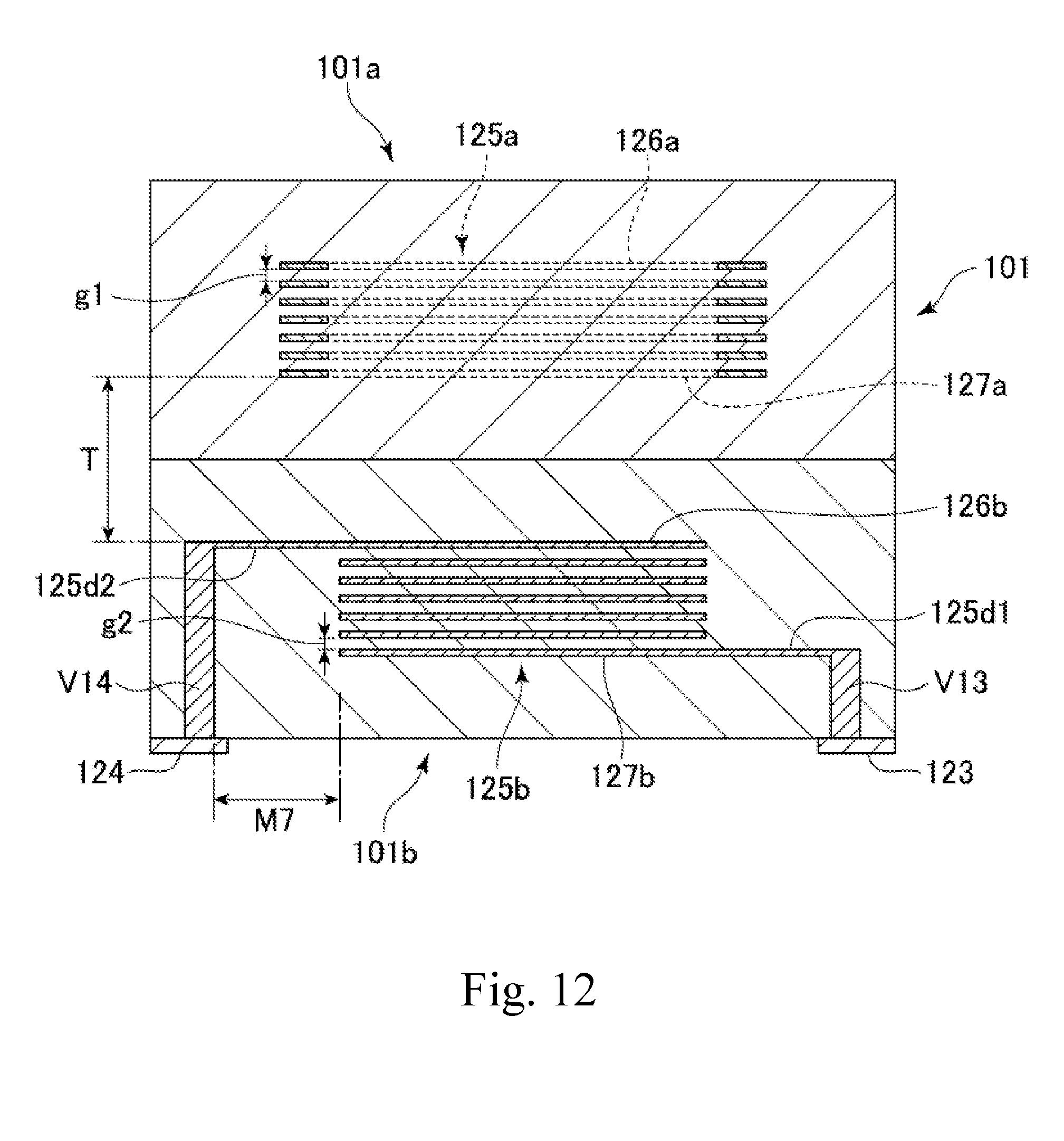
XML
uspto.report is an independent third-party trademark research tool that is not affiliated, endorsed, or sponsored by the United States Patent and Trademark Office (USPTO) or any other governmental organization. The information provided by uspto.report is based on publicly available data at the time of writing and is intended for informational purposes only.
While we strive to provide accurate and up-to-date information, we do not guarantee the accuracy, completeness, reliability, or suitability of the information displayed on this site. The use of this site is at your own risk. Any reliance you place on such information is therefore strictly at your own risk.
All official trademark data, including owner information, should be verified by visiting the official USPTO website at www.uspto.gov. This site is not intended to replace professional legal advice and should not be used as a substitute for consulting with a legal professional who is knowledgeable about trademark law.