Focal region optical elements for high-performance optical scanners
Axelrod; Noel ; et al.
U.S. patent application number 15/849696 was filed with the patent office on 2019-03-28 for focal region optical elements for high-performance optical scanners. The applicant listed for this patent is APPLE INC.. Invention is credited to Noel Axelrod, Refael Della Pergola.
| Application Number | 20190094531 15/849696 |
| Document ID | / |
| Family ID | 65806872 |
| Filed Date | 2019-03-28 |


| United States Patent Application | 20190094531 |
| Kind Code | A1 |
| Axelrod; Noel ; et al. | March 28, 2019 |
Focal region optical elements for high-performance optical scanners
Abstract
An optical device includes a light source, which is configured to emit a beam of light at a given wavelength, and at least one scanning mirror configured to scan the beam across a target scene. Light collection optics include a collection optic positioned to receive the light from the scene that is reflected from the at least one scanning mirror and to focus the collected light onto a focal plane, and a non-imaging optical element including a solid piece of a material that is transparent at the given wavelength, having a front surface positioned at the focal plane of the collection lens and a rear surface through which the guided light is emitted from the material in proximity to a sensor, so that the collected light is guided through the material and spread over the detection area of the sensor.
| Inventors: | Axelrod; Noel; (Jerusalem, IL) ; Della Pergola; Refael; (Jerusalem, IL) | ||||||||||
| Applicant: |
|
||||||||||
|---|---|---|---|---|---|---|---|---|---|---|---|
| Family ID: | 65806872 | ||||||||||
| Appl. No.: | 15/849696 | ||||||||||
| Filed: | December 21, 2017 |
Related U.S. Patent Documents
| Application Number | Filing Date | Patent Number | ||
|---|---|---|---|---|
| 62563703 | Sep 27, 2017 | |||
| Current U.S. Class: | 1/1 |
| Current CPC Class: | G02B 21/006 20130101; G02B 26/124 20130101; G02B 27/0994 20130101; G02B 19/0023 20130101; G01S 7/4816 20130101; G06K 7/10564 20130101; G02B 19/0076 20130101; G06K 7/10643 20130101; G02B 26/128 20130101; G01S 7/4817 20130101; G01S 17/42 20130101 |
| International Class: | G02B 26/12 20060101 G02B026/12; G06K 7/10 20060101 G06K007/10; G02B 21/00 20060101 G02B021/00 |
Claims
1. An optical device, comprising: a light source, which is configured to emit a beam of light at a given wavelength; at least one scanning mirror configured to scan the beam across a target scene; a sensor having a detection area; and light collection optics comprising: a collection optic positioned to receive the light from the scene that is reflected from the at least one scanning mirror and to focus the collected light onto a focal plane; and a non-imaging optical element comprising a solid piece of a material that is transparent at the given wavelength, having a front surface positioned at the focal plane of the collection lens and a rear surface through which the guided light is emitted from the material in proximity to the sensor, so that the collected light is guided through the material and spread over the detection area of the sensor.
2. The optical device according to claim 1, wherein the rear surface of the non-imaging optical element is in contact with the sensor.
3. The optical device according to claim 1, wherein the non-imaging optical element comprises a compound parabolic concentrator (CPC).
4. The optical device according to claim 1, wherein the material comprises silicon.
5. The optical device according to claim 1, wherein the material comprises glass.
6. The optical device according to claim 1, wherein the beam of light comprises a beam of light pulses, and wherein the sensor is configured to output a signal indicative of a time of incidence of a single photon on the sensor.
7. The optical device according to claim 6, and comprising a controller, which is configured to find times of flight of the light pulses to and from points in the scene responsively to the signal.
8. A method of sensing, comprising: scanning a beam of light at a given wavelength across a target scene using at least one scanning mirror; collecting the light from the scene that is reflected from the at least one scanning mirror and focusing the collected light onto a focal plane; and positioning a front surface of a non-imaging optical element, comprising a solid piece of a material that is transparent at the given wavelength, at the focal plane; and sensing the collected light using a sensor positioned in proximity to a rear surface of the non-imaging optical element, which spreads the collected light over a detection area of the sensor.
9. The method according to claim 8, wherein the sensor is positioned in contact with the rear surface of the non-imaging optical element.
10. The method according to claim 8, wherein the non-imaging optical element comprises a compound parabolic concentrator (CPC).
11. The method according to claim 8, wherein the material comprises silicon.
12. The method according to claim 8, wherein the material comprises glass.
13. The method according to claim 8, wherein the beam of light comprises a beam of light pulses, and sensing the collected light comprises sensing the light pulses and emitting a signal indicative of a time of incidence of a single photon on the sensor.
14. The method according to claim 13, and comprising finding times of flight of the light pulses to and from points in the target scene responsively to the signal.
Description
CROSS-REFERENCE TO RELATED APPLICATION
[0001] This application claims the benefit of U.S. Provisional Patent Application 62/563,703, filed Sep. 27, 2017, which is incorporated herein by reference.
FIELD OF THE INVENTION
[0002] The present invention relates generally to opto-electronic devices, and particularly to optical scanners.
BACKGROUND
[0003] Optical scanners are widely used for optically probing extended objects or target scenes. In a typical scanner a light source sends out a beam of light; the beam is scanned across the object by, for instance, a scanning mirror; then the light returned from the object is collected by collection optics and is directed to a sensor. The sensor emits a signal to a controller for further analysis.
[0004] High-performance optical scanners typically use both high-power light beams and high-speed scanners in order to sample and sense distant target scenes with high temporal and spatial resolution with a good signal-to-noise ratio.
SUMMARY
[0005] Embodiments of the present invention that are described hereinbelow provide improved optical scanners and methods for scanning.
[0006] There is therefore provided, in accordance with an embodiment of the invention, an optical device, including a light source, which is configured to emit a beam of light at a given wavelength, at least one scanning mirror configured to scan the beam across a target scene, and a sensor having a detection area. Light collection optics include a collection optic positioned to receive the light from the scene that is reflected from the at least one scanning mirror and to focus the collected light onto a focal plane. A non-imaging optical element includes a solid piece of a material that is transparent at the given wavelength, having a front surface positioned at the focal plane of the collection lens and a rear surface through which the guided light is emitted from the material in proximity to the sensor, so that the collected light is guided through the material and spread over the detection area of the sensor.
[0007] In a disclosed embodiment, the rear surface of the non-imaging optical element is in contact with the sensor, and the non-imaging optical element includes a compound parabolic concentrator (CPC). The material may include silicon or glass.
[0008] In some embodiments, the beam of light includes a beam of light pulses, and the sensor is configured to output a signal indicative of a time of incidence of a single photon on the sensor. A controller is configured to find times of flight of the light pulses to and from points in the scene responsively to the signal.
[0009] There is also provided, in accordance with an embodiment of the invention, a method of sensing, which includes scanning a beam of light at a given wavelength across a target scene using at least one scanning mirror. The light from the scene that is reflected from the at least one scanning mirror is collected and focused onto a focal plane. A front surface of a non-imaging optical element, including a solid piece of a material that is transparent at the given wavelength, is positioned at the focal plane. The collected light is sensed using a sensor positioned in proximity to a rear surface of the non-imaging optical element, which spreads the collected light over a detection area of the sensor.
[0010] The present invention will be more fully understood from the following detailed description of the embodiments thereof, taken together with the drawings in which:
BRIEF DESCRIPTION OF THE DRAWINGS
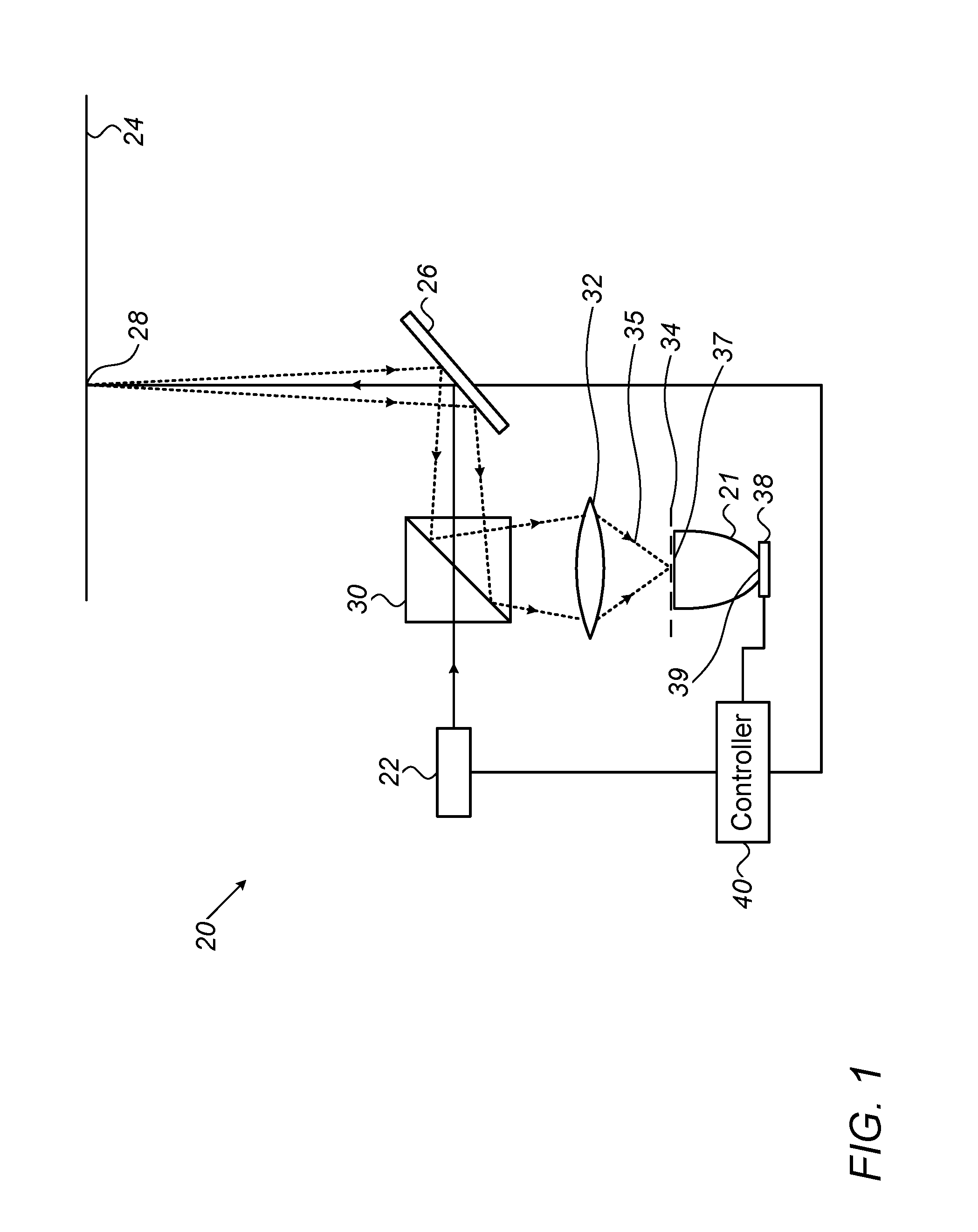
[0011] FIG. 1 is a schematic side view of an optical scanner with a non-imaging optical element, in accordance with an embodiment of the invention;
[0012] FIG. 2 is a schematic pictorial view of a non-imaging optical element, with optical rays traced through the element, in accordance with an embodiment of the invention; and
[0013] FIG. 3 is a schematic pictorial view of a non-imaging optical element, with optical rays traced through the element, in accordance with another embodiment of the invention.
DETAILED DESCRIPTION OF EMBODIMENTS
Overview
[0014] High-performance optical scanners, for instance light detection and ranging (LiDAR) sensors, typically use both high-intensity light beams and high-speed scanners in order to sample and sense distant target scenes with high spatial and temporal resolution with a good signal-to-noise ratio. The distance to the target scene may range from tens of centimeters to hundreds of meters.
[0015] The beam emitted by the light source is scanned across the target scene by a high-speed scanner, for instance by a rapidly oscillating scanning mirror. The light returned from the scene is reflected by a scanning mirror (either the scanning mirror described above or another mirror synchronized to the above mirror) towards a collection lens. An imaging collection lens focuses the returned light into a small spot on the sensor, and the signal emitted by the sensor is received by a controller for further analysis.
[0016] High-speed scanners are employed in this application to maximize the measurement rate. At very high angular speeds, the round-trip time for light can introduce a lag angle at the receiver. In order to compensate for deviations of the focused spot due to the scanner, a large sensing area is required. Furthermore, small focused spots of both returned light and scattered light have a very high irradiance that can damage the sensor and possibly degrade detection efficiency.
[0017] The lag angle .gamma. is given by the expression
.gamma.=2.tau..omega..sub.0.theta..sub.0,
wherein .omega..sub.0 and .theta..sub.0 are the scanner frequency and amplitude, respectively, and .tau. is the delay time, given by
.tau.=2R/c,
wherein R is the distance to the scene and c is the speed of light. The length L of the streak in the focal plane of the collection lens is given by the expression
L=2.gamma.f=4.tau..omega..sub.0.theta..sub.0f,
wherein f is the focal length of the collection lens.
[0018] The embodiments of the present invention that are described herein address the above limitations so as to enable high-speed, high-resolution optical scanners utilizing a sensor with high bandwidth, low dark noise, and reduced potential for damage and saturation. The disclosed embodiments use a non-imaging optical element, which is fabricated of a solid piece of dielectric material and is positioned between the focal plane of the collection optics and the sensor. This arrangement affords at least the following advantages: [0019] 1) The beam returned from the target scene and focused by the collection optics is spread on the sensor over an area that is larger than the spot in the focal plane; [0020] 2) The beam is stabilized on the sensor to a position that is essentially independent of the mirror speed and target distance; and [0021] 3) Using a solid piece of dielectric material for the non-imaging optical element increases its acceptance angle (numerical aperture). The use of a non-imaging optical element enables reducing the detection area of the sensor relative to what would otherwise be required in the absence of the non-imaging optics, as well as lowering the peak irradiance on the sensor. Both advantages result in larger signal bandwidth and longer detection ranges than could otherwise be achieved without the extra-focal elements.
[0022] The disclosed embodiments of the present invention provide optical scanners, wherein the light source can be either a non-laser source (such as a thermal source, a solid state source or a gas discharge source) or a laser source (either continuous-wave or pulsed). Such scanners can be used in depth-mapping systems, such as LIDARs, wherein the light source is a pulsed laser source, the sensor is a single-photon avalanche diode (SPAD), and a controller finds the distance to the target scene by time-of-flight analysis.
[0023] In alternative embodiments, other high-sensitivity sensors, such as an avalanche photodiode (APD), may be used.
System Description
[0024] FIG. 1 is a schematic side view of an optical scanner 20 with a non-imaging optical element 21, in accordance with an embodiment of the invention. The beam from a light source 22, such as, for example, a continuous-wave or pulsed laser, emitted at a given wavelength, is directed to a target scene 24 by a scanning mirror 26, forming and scanning an illumination spot 28 over the target scene. (The terms "light" and "illumination" are used herein to refer to any sort of optical radiation, including radiation in the visible, infrared, and ultraviolet ranges.) The light returned from illumination spot 28 is reflected by scanning mirror 26 and a beamsplitter 30 towards a collection lens 32, which focuses the light onto its focal plane 34 as rays 35.
[0025] Non-imaging optical element 21 has its front surface 37 positioned at or in proximity to focal plane 34 and its rear surface 39 at or in proximity to a sensor 38, such as a photodiode, a SPAD, or an APD. Non-imaging optical element 21 is fabricated of a solid piece of material that is transparent at the given wavelength and is configured to spread the light focused by collection lens 32 over the detection area of sensor 38. Front and rear surfaces 37 and 39, respectively, are coated with a suitable anti-reflection coating in order to minimize the reflection losses at these surfaces.
[0026] A controller 40 is connected to light source 22, scanning mirror 26, and sensor 38. Controller 40 typically comprises a programmable processor, which is programmed in software and/or firmware to carry out the functions that are described herein. Additionally or alternatively, at least some of the functions of controller 40 may be carried out by hardware logic circuits, which may be hard-wired or programmable. In either case, controller 40 has suitable interfaces for receiving data and transmitting instructions to other elements of the system as described. Thus, for example, controller 40 can be coupled to drive light source 22 and scanning mirror 26, as well as to receive and analyze signals emitted by sensor 38. In a LIDAR used for mapping the depth of target scene 24, for example, light source 22 comprises a pulsed laser, and sensor 38 comprises a SPAD. Controller 40 measures times of arrival of photons at sensor 38 relative to pulses emitted by light source 22 in order to derive time-of-flights across the target scene and thus to produce a depth map of the target scene.
[0027] As will be further detailed below, proper choice of non-imaging optical element 21 enables the use of a sensor 38 with a detection area having smaller dimensions than would be required if the sensor were located directly in focal plane 34. The use of a smaller detection area yields a higher bandwidth and a lower dark noise as compared to a larger sensor. Furthermore, non-imaging optical element 21 spreads the light focused at focal plane 34 over the detection area of sensor 38, thus alleviating problems that are associated with a high local irradiance.
[0028] FIG. 2 is a schematic pictorial view of non-imaging optical element 21, fabricated of solid silicon, with optical rays 35 traced through the element, in accordance with an embodiment of the invention. In this embodiment, non-imaging optical element 21 comprises a compound parabolic concentrator (CPC) and functions as a light-pipe to guide light from front surface 37 to rear surface 39.
[0029] A CPC is an optical element comprising a rotationally symmetrical surface around the optical axis, and planar front and rear surfaces perpendicular to the optical axis. The shape of the rotationally symmetrical surface is defined by rotating a section of a parabola (parabolic section) around an axis. This axis is defined as the perpendicular bisector of the line connecting the focal point of the parabola to the point of the parabolic section closest to the focal point. The surface defined by the rotation of this connecting line forms the rear surface of the CPC. The front surface of the CPC is determined by a suitable choice of the end-point of the parabolic section away from the rear surface. The maximal acceptance angle of a hollow CPC, i.e., a CPC that is filled with air, is typically tens of degrees, and is equal to the tilt angle between the axis of the parabola and the axis of rotation. The maximal acceptance angle for a solid CPC, i.e., a CPC fabricated of a solid piece of material, is increased from that of a hollow CPC with the same geometry due to the refraction of the optical rays at the front surface according to Snell's law. Consequently, a solid CPC is able to gather a larger angular extent of light than a hollow CPC. A hollow CPC is manufactured typically of glass or metal, and its inside is coated with a suitable reflective material, such as aluminum. A solid CPC is manufactured of a material that is transmissive at the wavelength of interest, and its rotationally symmetrical surface may be coated externally with a suitable reflective material, such as aluminum.
[0030] As shown in FIG. 1, non-imaging optical element 21 is positioned with front surface 37 at or in proximity to focal plane 34, and with rear surface 39 in contact with or in proximity to sensor 38.
[0031] In the present embodiment, non-imaging optical element 21 is fabricated of silicon, and is used in scanner 20 at a wavelength of 1550 nm. At this wavelength, silicon is highly transmitting, with an index of refraction of 3.5. Front and rear surfaces 37 and 39, respectively, are coated with a suitable anti-reflection coating in order to reduce reflection losses and to increase the overall transmission of non-imaging optical element 21. A rotationally symmetrical surface 50 of non-imaging optical element 21 does not require a reflective coating due to the high index of refraction of silicon, which ensures total internal reflection of rays 35.
[0032] Rays 35 impinge on front surface 37 at a point 52, chosen in this example as the center point of the front surface. Rays 35 propagate within non-imaging optical element 21, internally reflecting from rotationally symmetrical surface 50, and exiting through rear surface 39. At rear surface 39 rays 35 have spread out to a substantially larger area than at point 52 on front surface 37, thus alleviating the problems that are associated with a high local irradiance, were sensor 38 to be placed at focal plane 34. Rays impinging on other points on front surface 37 propagate similarly within non-imaging optical element 21 to rear surface 39.
[0033] Thus, independently of the position of focused rays in focal plane 34, all the rays transmitted by non-imaging optical element 21 arrive within the detection area of sensor 38, thus enabling the use of a sensor whose dimensions are independent of target distance and scan speed as long as the streak length L is less than the diameter of front surface 37. As an example, applying the equations presented above, a lag angle .gamma. of 0.75.degree. and a focal length f of 13.6 mm give a streak length L of 356 .mu.m. Thus for any scan speed and target distance yielding a lag angle not exceeding 0.75.degree., the diameter of front surface 37 does not have to exceed 356 .mu.m.
[0034] The condenser efficiency of non-imaging optical element 21, defined as the ratio between the areas of front surface 37 and rear surface 39, is 12.25. Consequently, sensor 38 can be substantially smaller than would be required if the sensor were positioned at focal plane 34.
[0035] The numerical aperture of rays accepted by the non-imaging optical element is 0.76. The transmittance of non-imaging optical element 21 is 98%.
[0036] FIG. 3 is a schematic pictorial view of a non-imaging optical element 60, fabricated of solid glass, with optical rays 35 traced through the element, in accordance with another embodiment of the invention. As in the preceding embodiment, non-imaging optical element 60 comprises a compound parabolic concentrator (CPC) functioning as a light-pipe to guide light from a front surface 62 to a rear surface 64 of the element. With reference to FIG. 1, non-imaging optical element 60 is positioned with front surface 62 at or in proximity to focal plane 34, and with rear surface 64 in contact with or in proximity to sensor 38.
[0037] Non-imaging optical element 60 is fabricated of solid glass. Similarly to non-imaging optical element 21 fabricated of silicon, front and rear surfaces 62 and 64are coated with a suitable anti-reflection coating in order to reduce reflection losses and to increase the overall transmission of non-imaging optical element 60. The transmittance of non-imaging optical element 60 fabricated of glass is 90%. A rotationally symmetrical surface 66 of non-imaging optical element 60 may be coated with a suitable reflective material, such as aluminum.
[0038] Rays 35 impinge on front surface 62 at a point 68, again chosen by way of example as the center point of the front surface. Rays 35 propagate within non-imaging optical element 60, internally reflecting from rotationally symmetrical surface 66, and exiting through rear surface 64. At rear surface 64 rays 35 have spread out to a substantially larger area than at point 68 on front surface 62, thus alleviating the problems that are associated with a high local irradiance. Rays impinging on other points on front surface 62 propagate similarly within non-imaging optical element 60 to rear surface 64. Thus, independently of the position of focused rays 35 in focal plane 34, all the rays transmitted by non-imaging optical element 60 arrive within the detection area of sensor 38, enabling the use of a sensor whose dimensions are independent of target distance and scan speed as long as the streak length L is less than the diameter of front surface 62.
[0039] The condenser efficiency of non-imaging optical element 60 is 4, the numerical aperture is 0.76, and non-imaging optical element 21 can accept a lag angle y of 0.4.degree..
[0040] Although non-imaging optical elements 21 and 60 both comprise a CPC, other embodiments of the present invention can use other sorts of non-imaging optical elements comprising a solid piece of a material that are known in the art, such as various sorts of light-pipes.
[0041] It will thus be appreciated that the embodiments described above are cited by way of example, and that the present invention is not limited to what has been particularly shown and described hereinabove. Rather, the scope of the present invention includes both combinations and subcombinations of the various features described hereinabove, as well as variations and modifications thereof which would occur to persons skilled in the art upon reading the foregoing description and which are not disclosed in the prior art.
* * * * *
D00000
D00001
D00002
XML
uspto.report is an independent third-party trademark research tool that is not affiliated, endorsed, or sponsored by the United States Patent and Trademark Office (USPTO) or any other governmental organization. The information provided by uspto.report is based on publicly available data at the time of writing and is intended for informational purposes only.
While we strive to provide accurate and up-to-date information, we do not guarantee the accuracy, completeness, reliability, or suitability of the information displayed on this site. The use of this site is at your own risk. Any reliance you place on such information is therefore strictly at your own risk.
All official trademark data, including owner information, should be verified by visiting the official USPTO website at www.uspto.gov. This site is not intended to replace professional legal advice and should not be used as a substitute for consulting with a legal professional who is knowledgeable about trademark law.