Microscopy Imaging
Fine; Alan Marc ; et al.
U.S. patent application number 16/113578 was filed with the patent office on 2019-03-28 for microscopy imaging. This patent application is currently assigned to Alentic Microscience Inc.. The applicant listed for this patent is Alentic Microscience Inc.. Invention is credited to Alan Marc Fine, Peter Hodges Gregson.
| Application Number | 20190094509 16/113578 |
| Document ID | / |
| Family ID | 43898090 |
| Filed Date | 2019-03-28 |
View All Diagrams
| United States Patent Application | 20190094509 |
| Kind Code | A1 |
| Fine; Alan Marc ; et al. | March 28, 2019 |
MICROSCOPY IMAGING
Abstract
Among other things, an imaging device has a photosensitive array of pixels, and a surface associated with the array is configured to receive a specimen with at least a part of the specimen at a distance from the surface equivalent to less than about half of an average width of the pixels.
| Inventors: | Fine; Alan Marc; (Prospect, CA) ; Gregson; Peter Hodges; (Halifax, CA) | ||||||||||
| Applicant: |
|
||||||||||
|---|---|---|---|---|---|---|---|---|---|---|---|
| Assignee: | Alentic Microscience Inc. Halifax CA |
||||||||||
| Family ID: | 43898090 | ||||||||||
| Appl. No.: | 16/113578 | ||||||||||
| Filed: | August 27, 2018 |
Related U.S. Patent Documents
| Application Number | Filing Date | Patent Number | ||
|---|---|---|---|---|
| 15642434 | Jul 6, 2017 | 10114203 | ||
| 16113578 | ||||
| 14698532 | Apr 28, 2015 | 9720217 | ||
| 15642434 | ||||
| 12913639 | Oct 27, 2010 | 9041790 | ||
| 14698532 | ||||
| 61255781 | Oct 28, 2009 | |||
| Current U.S. Class: | 1/1 |
| Current CPC Class: | G02B 21/0008 20130101 |
| International Class: | G02B 21/00 20060101 G02B021/00 |
Claims
1-8. (canceled)
9. An apparatus comprising a housing, a lid hinged to the housing, the housing and the lid enclosing a space, within the enclosed space and facing the lid, a sensor having an array of photosensitive elements exposed at a surface, the surface being configured to receive a specimen within a near field distance of the photosensitive elements, the hinged lid configured to give access to the space to permit placement of the specimen on the surface of the sensor, and on the lid and facing the sensor, a light source containing an array of LEDs, the array being configured to be controlled singly or in groups to illuminate the specimen at different wavelengths and positions relative to the surface of the sensor.
10. The apparatus of claim 9 in which the LEDs comprise OLEDs.
11. The apparatus of claim 9 comprising a controller configured to control the LEDs.
12. The apparatus of claim 11 in which the controller is within the space enclosed by the housing and the lid.
13. The apparatus of claim 11 in which the controller comprises a microprocessor of a computing device.
14. The apparatus of claim 9 in which the array of LEDs, the specimen, and the sensor are aligned for conventional microscopy.
15. The apparatus of claim 9 in which the array of LEDs, the specimen, and the sensor are aligned for dark-field microscopy in which the specimen is illuminated from an angle outside the acceptance angle of the photosensitive elements.
16. The apparatus of claim 9 in which the array of LEDs is interchangeable.
17. The apparatus of claim 9 in which the LEDs comprise AMOLEDs.
18. The apparatus of claim 11 in which the controller is configured to selectively excite one or more LEDs simultaneously or in sequence.
19. A method comprising opening a hinged lid associated with the housing, placing a specimen on a surface of an array of photosensitive elements within a near field distance of the photosensitive elements, closing the hinged lid, controlling an array of LEDs to illuminate the specimen, and capturing an image of the specimen formed at the array of photosensitive elements by the illumination of the array of LEDs.
20. An apparatus comprising a sensor having an array of light-sensitive elements exposed at a surface of the sensor configured to receive, within a near field distance of the surface of the sensor, a specimen to be analyzed, an adhesive layer on the surface of the sensor and configured to adhere to elements of the sensor.
21. The apparatus of claim 20 in which the adhesive layer comprises molecules having specific affinities.
22. The apparatus of claim 21 in which the adhesive layer is configured to exclude particular elements of the specimen.
23. The apparatus of claim 22 in which the particular elements of the specimen comprise cells.
24. The apparatus of claim 21 in which the adhesive layer is configured to enrich particular elements of the specimen.
25. The apparatus of claim 20 in which the adhesive layer comprises elements for binding assays.
26. The apparatus of claim 25 in which the elements for the binding assays comprise fluorophores.
27. The apparatus of claim 25 in which the elements for the binding assays comprise nanoparticles or microbeads.
28. An apparatus comprising a sensor having an array of light-sensitive elements exposed at a surface of the sensor configured to receive, within a near field distance of the surface of the sensor, a specimen to be analyzed, a layer of light-transmissive material on the surface containing elements that are responsive to light.
29. The apparatus of claim 28 in which the elements that are responsive to light comprise fluorophores.
30. The apparatus of claim 28 in which the elements that are responsive to light comprise phosphors.
31. The apparatus of claim 28 in which the elements that are responsive to light comprise up-converters.
32. The apparatus of claim 28 in which the elements that are responsive to light comprise molecules excited at one wavelength and emitting at another wavelength.
33. The apparatus of claim 28 in which the light-sensitive elements have ranges of spectral sensitivity, the elements comprise fluorophores, and the fluorophores are excited by wavelengths outside the ranges of spectral sensitivity and are emitting within the ranges of spectral sensitivity.
34. The apparatus of claim 33 in which the fluorophores are excited in the x-ray spectrum.
Description
CROSS-REFERENCE TO RELATED APPLICATIONS
[0001] This application is a continuation (and claims the benefit of priority under 35 USC 120) of U.S. application Ser. No. 15/642,434, filed on Jul. 6, 2017, which claims the benefit of U.S. application Ser. No. 14/698,532, filed on Apr. 28, 2015, now U.S. Pat. No. 9,720,217 issued on Aug. 1, 2017, which claims the benefit of U.S. application Ser. No. 12/913,639, filed Oct. 27, 2010, now U.S. Pat. No. 9,041,790 issued on May 26, 2015, which claims the benefit of the filing date of U.S. provisional application Ser. 61/255,781, filed Oct. 28, 2009, "Contact Optical Microscopy", which are all incorporated here by reference in their entireties.
BACKGROUND
[0002] Microscopy in its various forms is an essential tool in an ever-growing range of human activity, from basic research in the natural sciences, industrial research and development, process and quality control, forensics and biosafety, to clinical human and veterinary medical diagnostics, among others. The most widely used form of microscopy is optical. The resolution of standard forms of optical microscopy, however, is limited to several hundred nanometers by the diffraction of light between the specimen and the microscope objective lens. Due to its wave properties, light passing through a circular lens creates a ring-shaped diffraction pattern; the images of two different points formed by such a lens can be resolved if the principal diffraction maximum of one point lies outside of the first minimum of the other point. This theoretical diffraction limit, also known as the Abbe limit or Rayleigh criterion, is approximately equal to 0.61.lamda./NA, where .lamda. is the wavelength of the light and NA is the numerical aperture of the lens, given by
NA=n sin .alpha.
where n is the index of refraction of the optical medium between the lens and the specimen and .alpha. is the half-angle of acceptance of the lens. Currently available microscope objective lenses typically have NA<1.4, so that the theoretical diffraction limit for visible light is >200 nm; in practice the resolution limit of standard optical microscopes, compromised by various lens aberrations, is poorer, seldom much below 0.5 .mu.m.
[0003] A variety of approaches have been taken to reduce or overcome the diffraction limit. NA can be increased by use of high refractive index media. The size of an illumination spot can be reduced by strategies such as stimulated emission depletion (STED), or the positions of sparse individual molecules can be approximated by the centers of their diffracted images.
[0004] Near-field scanning optical microscopes (NSOMs) can overcome the diffraction limit by using a probe having a tip smaller than the wavelength of light and positioned less than a wavelength from the specimen. In a typical configuration, the probe tip or aperture is scanned along the specimen close to its surface to map the near field produced by fluorescence at the specimen surface. NSOM imaging is non-destructive and can be carried out in an aqueous environment, permitting observation of living cells and hydrated molecules.
[0005] Other methods exist that do not require scanning, but instead require a superlens. Lensless microscopy methods are known, however they may require integration of multiple images or subsequent computational image derivation in order to produce usable images.
SUMMARY
[0006] In general, in an aspect, an imaging device has a photosensitive array of pixels, and a surface associated with the array is configured to receive a specimen with at least a part of the specimen at a distance from the surface equivalent to less than about half of an average width of the pixels.
[0007] Implementations may include one or more of the following features. The specimen is included. There is a light source. A specimen chamber adjacent the surface is defined in part by a wall that is spaced apart from the surface and transmits light to illuminate the specimen. A fluid channel carries a fluid specimen into the chamber. The chamber is sealed against leakage of fluid. A second fluid channel carries the fluid specimen out of the chamber. There is a reservoir for the fluid specimen and a pump to pump the fluid specimen from the reservoir and into and out of the chamber. There is an imaging integrated circuit. The integrated circuit is back-side illuminated. A computer-based system uses a program to display, analyze, or store high-resolution images of the specimen using information derived from the device.
[0008] The specimen comprises a solid. The specimen comprises a liquid or is suspended or dissolved in a liquid. The wall has at least one electrode adjacent to the chamber. The wall has a heating element adjacent to the chamber. The wall has a temperature probe adjacent to the chamber. The wall has a pH probe adjacent to the chamber. The wall is at least partially translucent. The light source is positioned so that a path of light from the light source to the surface is at an angle of 45 degrees or more to the surface. The light source is positioned so that a path of light from the light source to the surface is at an angle of at most 45 degrees to the surface. The light source is positioned so that a path of light from the light source to the surface is approximately parallel to the surface. The light source comprises light-emitting diodes. The light source comprises ambient light. The light source comprises a portable multi-color light source.
[0009] There is a layer of transparent chemically resistant material on the surface. The chemically resistant material comprises diamond. The chemically resistant material comprises Al.sub.2O.sub.3. The chemically resistant material comprises Si.sub.3N.sub.4. There is a layer of wavelength-filtering material on the surface. A layer of light-transmissive material contains fluorophores on the surface. The specimen emits light. There is a layer of polarizing material coating the surface. A layer of adhesive material coats the surface. The photosensitive array provides a high resolution.
[0010] In general, in an aspect, an imaging device has a photosensitive array, and a surface associated with the array is configured to receive a specimen with at least a part of the specimen at a distance from the photosensitive array that satisfies or at least approximately satisfies a near-field criterion.
[0011] In general, in an aspect, at least a part of a specimen is placed at a distance, from a surface associated with a photosensitive array of pixels, that is equivalent to less than about half of an average width of the pixels, and signals generated by the photosensitive array are used to produce a high resolution image of the specimen.
[0012] Among other advantages of these and other aspects and features are the following. These approaches in devices are simple, easy to use, not cumbersome, have broad applicability to a very wide range of applications, are relatively inexpensive and rapid. In some implementations, they are suitable for imaging of moving or rapidly changing specimens. Difficult to fabricate inexpensive optical elements may not be required.
[0013] These and other features and aspects, and combinations of them, may be expressed as methods, systems, components, means and steps for performing functions, business methods, program products, and in other ways.
[0014] Other advantages and features will become apparent from the following description and from the claims.
DESCRIPTION
[0015] FIG. 1 shows a top view of an imaging device.
[0016] FIG. 2 shows a section view of an imaging device.
[0017] FIG. 3 shows a top view of an imaging integrated circuit.
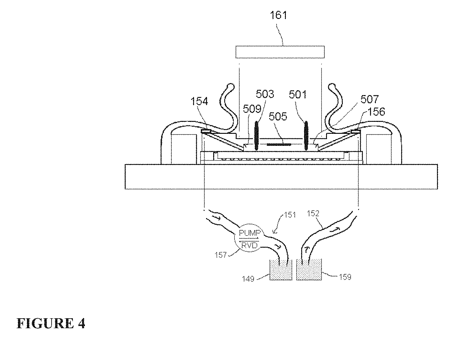
[0018] FIG. 4 shows a section view of an imaging device equipped with a light source, a probe, electrodes, a heating element, and a fluid flow system.
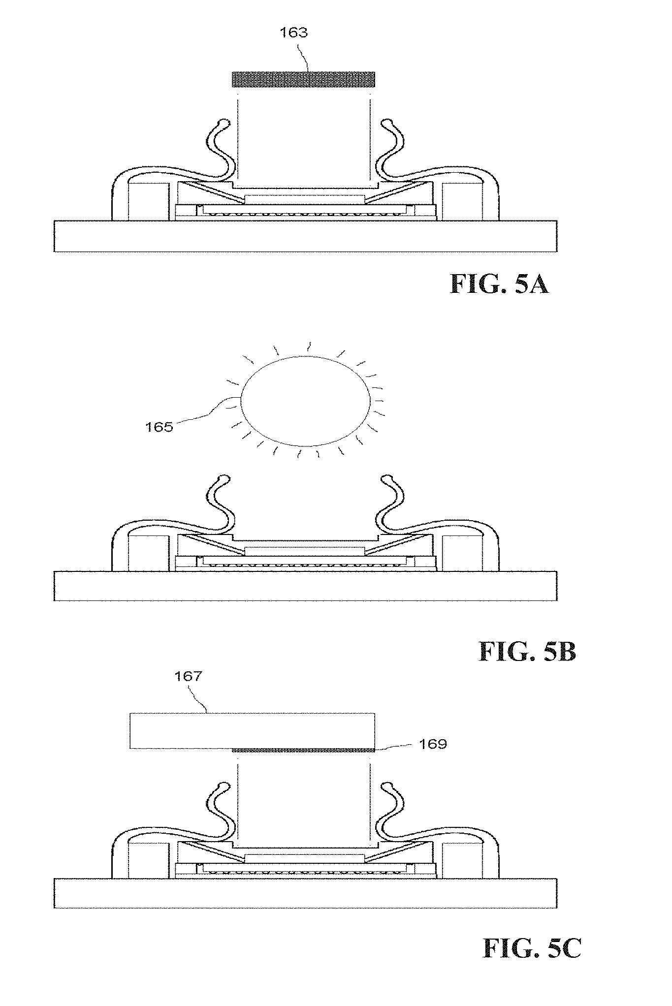
[0019] FIGS. 5A, 5B, and 5C show section views of an imaging device with light sources: light-emitting diodes (FIG. 5A), ambient (FIG. 5B), and portable multi-color (FIG. 5C).
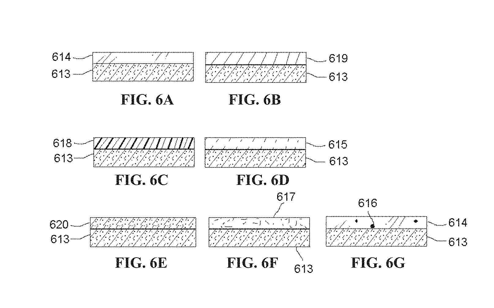
[0020] FIGS. 6A through 6G show section views of an imaging integrated circuit with coatings: transparent, wavelength-filtering or polarizing (FIG. 6A), metallic (FIG. 6B), plastic (FIG. 6C), transparent chemically resistant (FIG. 6D), nonconductor (FIG. 6E), adhesive (FIG. 6F), and transparent having fluorophores, scintillants or phosphors (FIG. 6G).
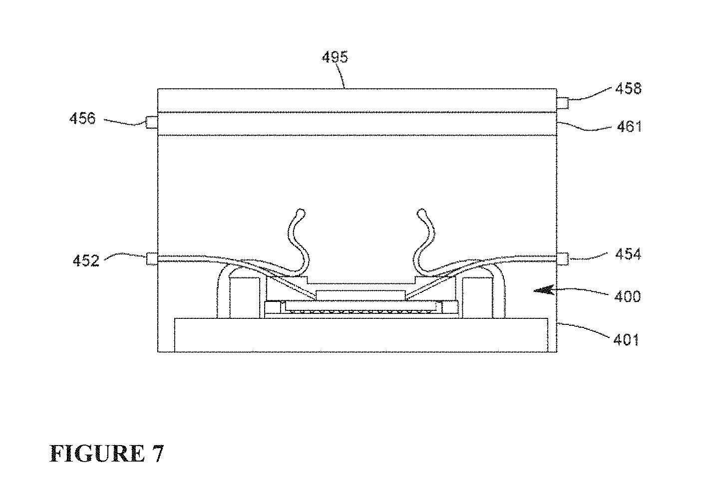
[0021] FIG. 7 shows a section view of an imaging device equipped with a portable multi-color light source and a housing with power, I/O, and fluid connectors.
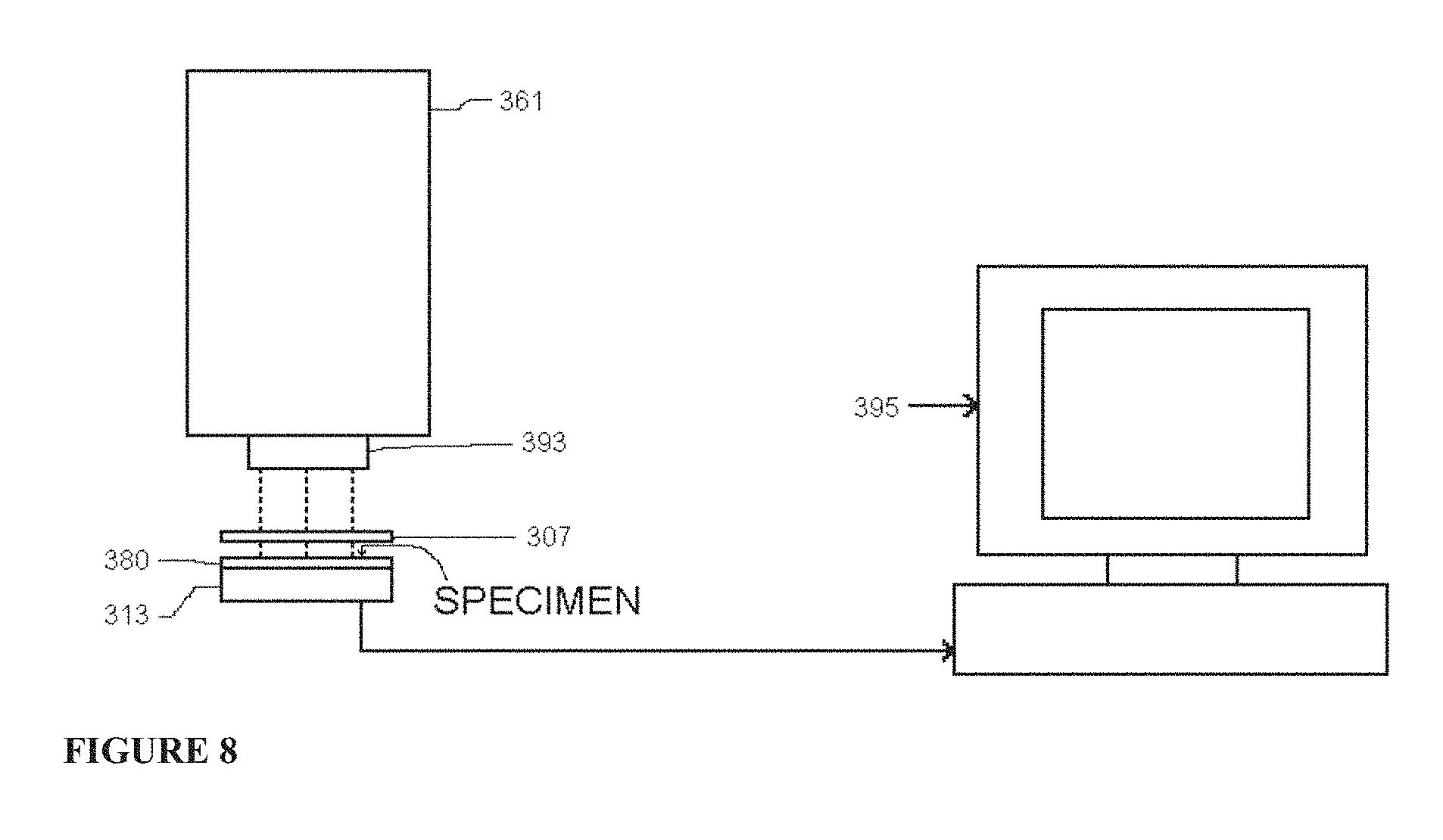
[0022] FIG. 8 shows a schematic of an imaging device and a computer-based system, with dashed lines indicating light along the optical path.
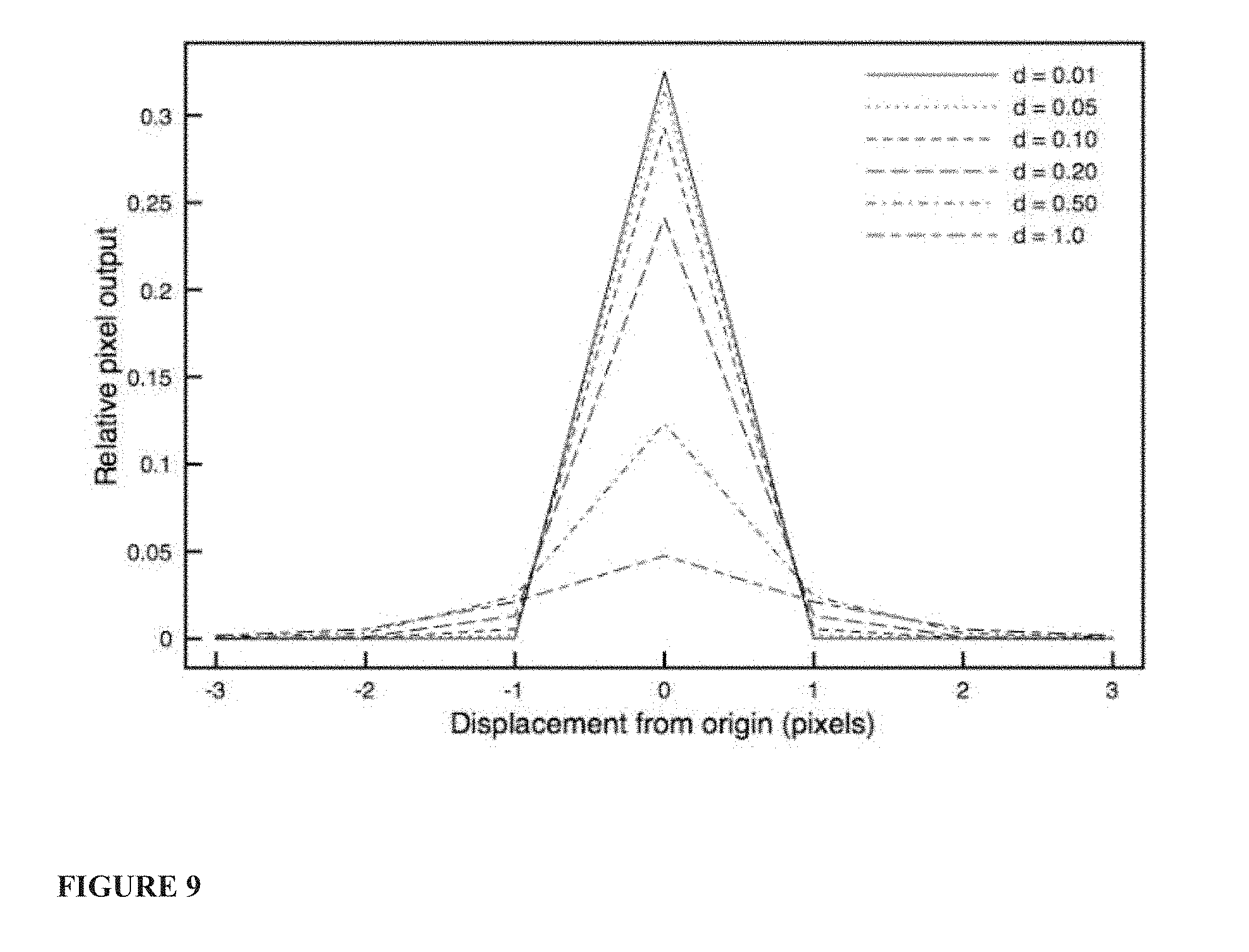
[0023] FIG. 9 shows a computed plot of a pixel response due to light from a point source passing into an imaging integrated circuit constructed in silicon at various distances from a center of a middle pixel (origin) as the distance (elevation) of the source above that center is increased. Distance, both laterally and above the surface, is measured in units of the width of a pixel. Each curve represents a relation for a specified vertical distance of the source above the photosensitive surface of the imaging integrated circuit, as indicated in the inset key.
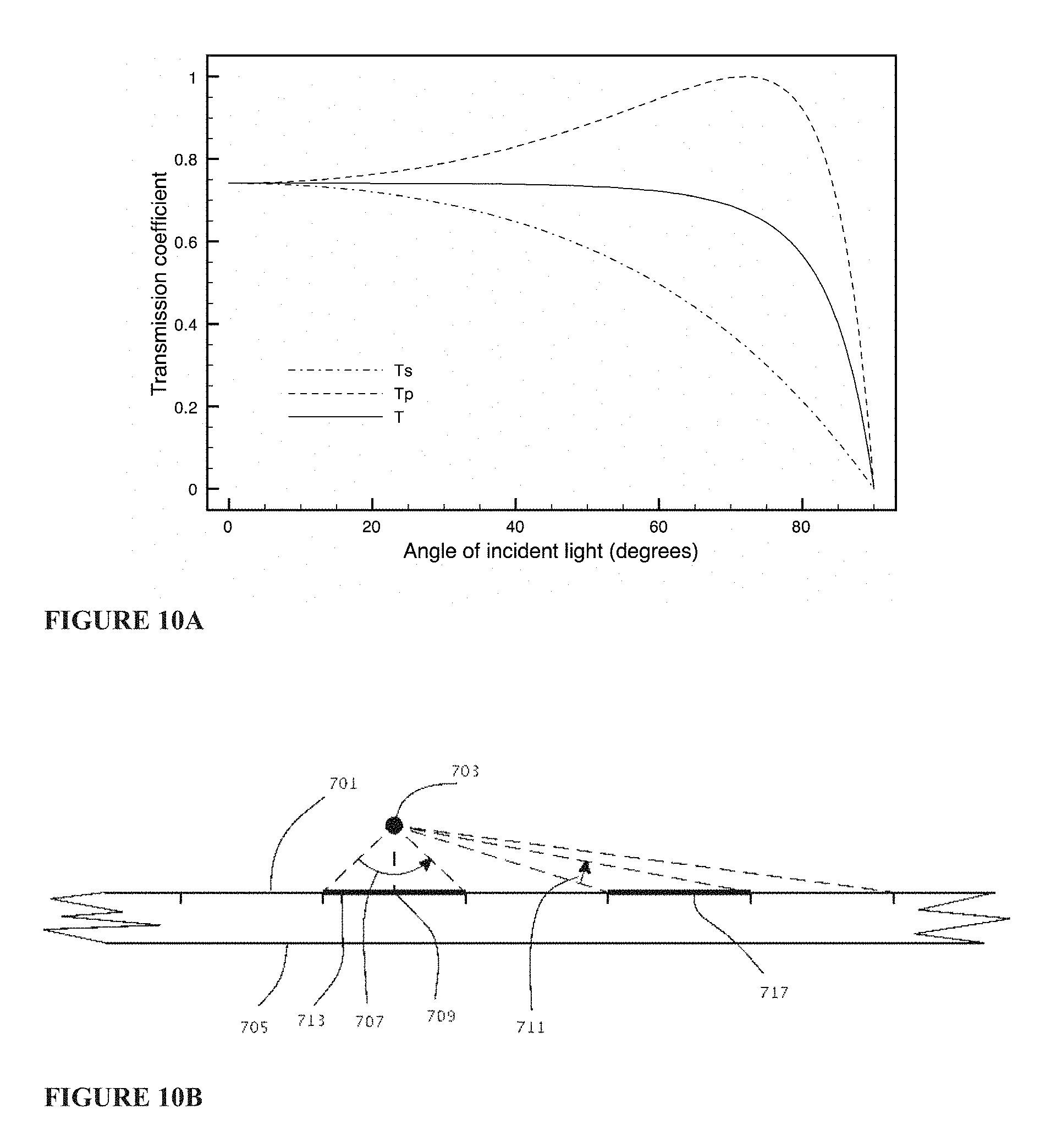
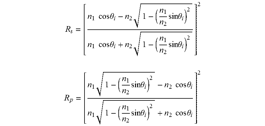
[0024] FIGS. 10A and 10B show (10A) transmission coefficients of the Fresnel formulas for angles between zero and ninety degrees; (10B) an illustration of decreasing pixel profile with respect to a light source as angle of light with respect to the surface normal increases.
[0025] FIG. 11 is an image of a 30 .mu.m-thick Mylar sheet, imaged using an apparatus referred to in the Examples, having 5.2 .mu.m.times.5.2 .mu.m pixels.
[0026] FIG. 12 is an image of micro-droplets in an aerosol of organic solvent, imaged using an apparatus referred to in the Examples, having 5.2 .mu.m.times.5.2 .mu.m pixels.
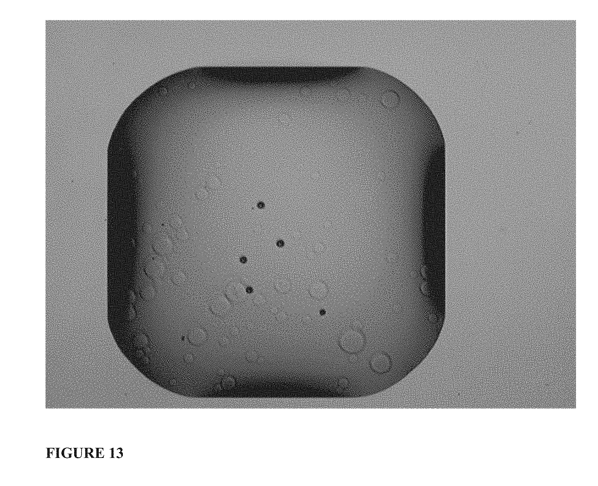
[0027] FIG. 13 is an image of a 1 .mu.l droplet of water with suspended Sephadex beads of sizes ranging from <20 .mu.m to >100 .mu.m, imaged using an apparatus referred to in the Examples, having 5.2 .mu.m.times.5.2 .mu.m pixels.
[0028] FIG. 14 is an image of a sample of fresh, living, unstained blood from an African clawed frog (Xenopus laevis), diluted in calcium-free Ringer's solution, imaged using an apparatus referred to in the Examples, with pixels 2.2 .mu.m.times.2.2 .mu.m. A full field of view (3.2.times.2.4 mm) is shown, along with a "zoomed in" view of part of the field of view, in which the elliptical shape and nucleated structure of the erythrocytes (long axis .about.24 .mu.m, short axis .about.16 .mu.m) is evident. The zoomed image has been enhanced by 2.times.2 pixel augmentation with bicubic interpolation.
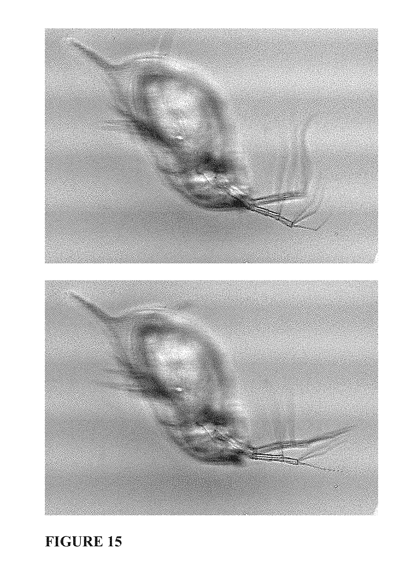
[0029] FIG. 15 is a portion of the field of view of two frames of a video sequence of a living water flea (Daphnia sp.), imaged using an apparatus referred to in the Examples, with pixels 2.2 .mu.m.times.2.2 .mu.m.
FIGURE LEGEND
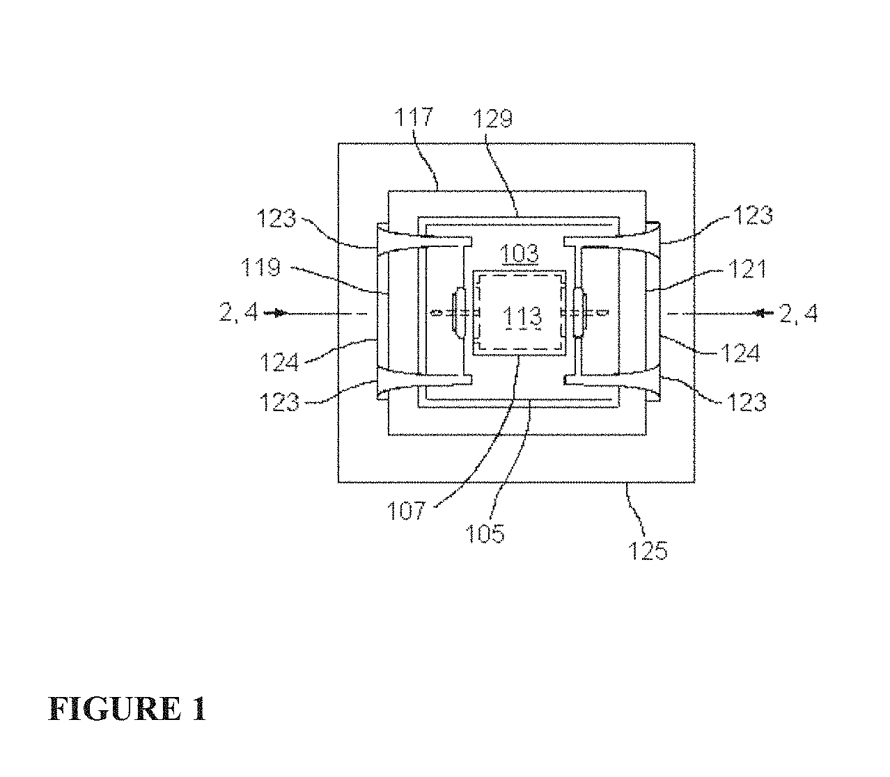
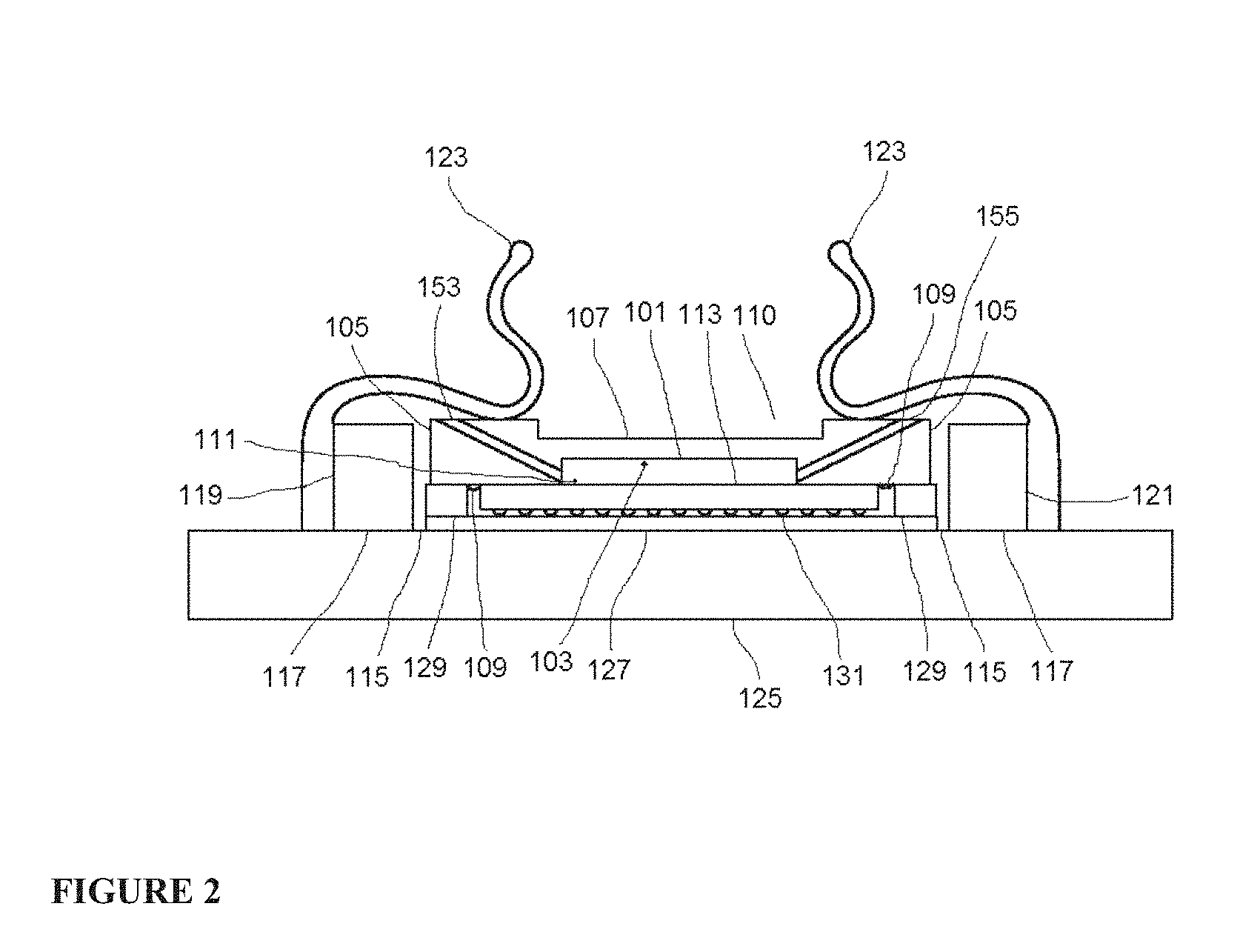
[0030] 101 Specimen chamber [0031] 103 Chamber lid [0032] 105 Walls of chamber lid [0033] 107 Top of chamber lid [0034] 109 Rubberized gasket [0035] 110 Recess [0036] 111 Photosensitive surface [0037] 113 Imaging integrated circuit [0038] 115 Space [0039] 117 Locating block [0040] 119 Side of locating block [0041] 121 Opposite side of locating block [0042] 123 Spring clips [0043] 124 Base of spring clips [0044] 125 Mounting block [0045] 127 Printed circuit headboard [0046] 129 Shim [0047] 131 Solder pads [0048] 149 Waste chamber [0049] 151 Fluid flow system [0050] 152 Tubing [0051] 153 First fluid channel [0052] 154 First connector [0053] 155 Second fluid channel [0054] 156 Second connector [0055] 157 Pump [0056] 159 Reservoir [0057] 161 Light source [0058] 163 LEDs [0059] 165 Ambient light source [0060] 167 Portable multi-color light source [0061] 169 Display for portable multi-color light source [0062] 203 High-resolution photosensitive pixel array [0063] 205 Supporting circuitry [0064] 207 Pixel(s) [0065] 307 Cover [0066] 313 Imaging integrated circuit [0067] 361 Light source [0068] 380 Coating [0069] 393 Collimator [0070] 395 Computer-based system [0071] 400 Imaging device [0072] 401 Housing [0073] 452 Input connector for fluid flow system [0074] 454 Output connector for fluid flow system [0075] 456 Input/output connector [0076] 458 Power connector [0077] 461 OLED light source [0078] 495 Circuitry for input/output and illumination control [0079] 501 Temperature probe [0080] 503 pH probe [0081] 505 Heating element [0082] 507 Electrode [0083] 509 Second electrode [0084] 613 Imaging integrated circuit [0085] 614 Transparent coating, wavelength-filtering or polarizing material [0086] 615 Transparent chemically resistant material (diamond, Al.sub.2O.sub.3, Si.sub.3N.sub.4), transparent [0087] mechanically resistant material [0088] 616 Fluorophore, phosphor or scintillant [0089] 617 Adhesive coating [0090] 618 Plastic coating [0091] 619 Metallic coating, surface plasmon generating material [0092] 620 Passivation layer [0093] 701 Photosensitive array having pixels [0094] 703 Point source of light [0095] 705 VLSI circuit [0096] 707 Angle [0097] 709 Origin [0098] 711 Second angle [0099] 713 Pixel immediately under light source [0100] 717 Pixel not immediately under light source Among other things, we describe an imaging apparatus that achieves resolution beyond the classical diffraction limits of conventional microscopy by utilizing an imaging integrated circuit having a high-resolution photosensitive array and supporting circuitry for readout. Spatial resolution is not limited by the diffraction limit as is inherent in most optical systems. No lenses or computational correction algorithms are required to produce high-resolution images.
[0101] The devices and methods described here can yield high-resolution images of a specimen without the need for lenses or computational image correction. Images are captured using an imaging integrated circuit having a high-resolution photosensitive array of pixels presenting a photosensitive surface, with supporting circuitry for readout, and associated computing equipment for data processing and user interaction. Light sources may be ambient or provided in an apparatus as appropriate. For parts of the specimen within half a pixel width of the photosensitive surface, the resolution of the image is limited by the size of the pixels making up the photosensitive surface. If the average width of these pixels is less than about half the wavelength of the light being used and the specimen is within half a pixel width of the photosensitive surface, then the near-field criterion may be satisfied and images can be obtained that equal or exceed the resolution of standard lens-based optical microscopes. The near-field criterion may be considered to be reached, for example, when the distance between the photosensitive surface and the specimen is less than the wavelength of interest.
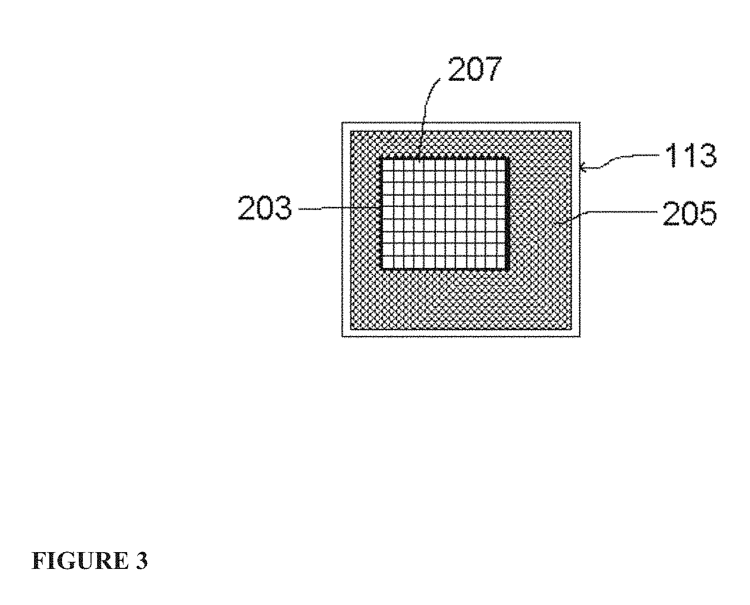
[0102] Embodiments of imaging devices are illustrated by the examples shown in FIGS. 1, 2, 3, 4, 5, 6, 7 and 8. In some implementations, the imaging device may be oriented such that specimens are brought closer to the photosensitive surface by the force of gravity. In some embodiments, the imaging device is inverted or mounted on its side vertically, incorporating when necessary a restraint (not shown) for specimens in the specimen chamber. A cavity denoted specimen chamber 101 is formed by a chamber lid 103 having walls 105 and top 107, and by a photosensitive surface 111 presented by an imaging integrated circuit 113.
[0103] In some examples, the chamber lid may be made of any material that is rigid enough to resist warping or cracking under pressure. In some embodiments, the chamber lid 103 is at least partially transmissive of light. In some embodiments, the walls 105 are made of opaque material (examples include metal and ceramic) and the top 107 is either absent or made of transparent material. In some embodiments, the chamber lid 103 is made of glass or polystyrene and the top is between about 0.5 mm and about 1 mm in thickness. The walls of the chamber lid are of such dimensions and thickness as to approximately enclose the photosensitive surface in their inside dimensions and to approximately enclose the imaging integrated circuit in their outside dimensions. In some embodiments, the walls of the chamber lid are rectangular and each wall of the chamber lid has an inside length less than about 10 mm. The distance between the top 107 of the chamber lid 103 and the surface 111 is preferably between about 50 .mu.m and about 1 mm, more preferably between about 75 .mu.m and about 250 .mu.m. In some embodiments, the top 107 achieves the desired specimen chamber height in the region of a recess 110 with respect to the height of the walls 105; in some embodiments, the recess is either absent, or no larger than necessary to receive a light source 161. A surface of the bottom 109 of the chamber lid 103 may be rubberized with a gasket or treated with a water-resistant microlayer, to assure a fluid-tight pressure-resistant seal when pressed down upon the non-photosensitive ceramic or plastic package of the imaging integrated circuit 113 by spring clips 123. The specimen chamber holds the specimen and medium in which the specimen is carried. For dry specimens, the medium may be air or some other gas or gas mixture appropriate to the stability or properties of the specimen. For liquid specimens or specimens suspended or dissolved in liquid, the medium is an appropriate liquid; the chamber need not be voided of gas in order to obtain images of such specimens.
[0104] The imaging integrated circuit 113, a very-large-scale integrated (VLSI) circuit, has a high-resolution photosensitive array 203 including a two-dimensional array of pixels presented at its surface 111, surrounded by non-photosensitive supporting circuitry 205 for readout. The imaging integrated circuit 113 (including packaging) is electrically and mechanically attached to the headboard 127, which is a printed circuit board whose components connect to circuitry on the mounting block 125. The imaging integrated circuit 113 makes electronic and mechanical connection to the headboard 127 by means of a multiplicity of solder pads 131. Integrated circuit packaging for such purposes includes but is not limited to ball grid arrays, quad flat packs, and leadless chip carriers. The array 203 is made of materials used in very-large-scale or larger integrated circuits; in some embodiments, the array is substantially germanium, gallium nitride, or gallium arsenide. In some embodiments, the array is substantially silicon. In some embodiments, the high-resolution photosensitive array comprises a charge-coupled device (CCD); in other embodiments, the high-resolution photosensitive array is fabricated in CMOS. As an illustrative example, the OmniVision OV5642 imaging integrated circuit has area dimensions approximately 6.96 mm.times.6.71 mm, surrounding a photosensitive array approximately 3.67 mm.times.2.73 mm in area. This array is near centered, having a center with respect to the IC center (0,0) at about (220, 445) .mu.m.
[0105] The chamber lid 103 is positioned in place within a space 115 defined by a rectangular locating block 117. Both the locating block 117 and the imaging integrated circuit 113 on its headboard 127 are situated atop the mounting block 125. The mounting block 125 is large enough in area to accommodate the dimensions of the locating block plus the spring clips 123. The locating block 117 is bonded to the mounting block 125 by means of solder, adhesive, or screws. In some embodiments, the locating block is made of a rigid, opaque material (examples of which include plastic, metal, or fiberglass) of about 1-2 mm thickness, with length dimensions of at most about 0.5 mm larger than those of the chamber lid walls. Two or more adjacent spring clips 11 are bonded to mounting block 125 at their bases 124, and they overlay locating block 117 and at least part of the walls 105 of the chamber lid 103, holding the lid in place inside the space 115. There are two spring clips 123 on each of two opposite sides 119, 121 of the locating block. The spring clips on each side are oriented in parallel and are of such shape as to facilitate insertion and removal of specimens and the chamber lid 103 when not in operation, but to maintain the lid in place during operation. In some embodiments, the spring clips are metal. In some embodiments, the spring clips are plastic. In some embodiments, the chamber lid is held in the space by means of other fasteners such as, for example, screws or slides adapted to the inside of the locating block. The outside edge of the imaging integrated circuit 113 is surrounded by a rectangular shim 129 of height approximately equal to the circuit's height and thickness equal to the remainder of the space 115 not occupied by the imaging integrated circuit. The shim 129 is made of suitable shimming material; as examples, the shim can be made of plastic, phenolic, fiberglass, or metal. The shim 129 is bonded to the mounting block 125 by means of solder, adhesive, or screws; it is also bonded to the outside edge of the imaging integrated circuit 113 by means of injected latex, silicone, plastic (preferably polystyrene), or adhesive so as to maintain a fluid-tight seal with the imaging integrated circuit.
[0106] One or more angled fluid channels are situated each having one lower end opening into the specimen chamber and the other, upper end positioned so as to allow flow of liquid specimen into or out of the specimen chamber, as appropriate. In some embodiments, there is a first fluid channel 153 and a second fluid channel 155 situated opposite each other within the walls 105 of the specimen chamber 103. These fluid channels have diameter slightly less than the height of the specimen chamber. They are, for example, cylindrical and oriented at an angle, for example, about 45 degrees with respect to the surface 111, permitting passage of fluid from the outside of the device into the specimen chamber. In some embodiments, a fluid flow system 151 is connected to fluid channels 153, 155 by tubing 152 and respective connectors 154,156, e.g. micro-Luer-Lok hubs. The fluid flow system 151 includes the tubing 152, a pump 157 that is preferably reversible and capable of variable flow rate, a reservoir 159, and a waste chamber 149. The tubing is preferably fused silica or plastic. In some embodiments, there are several pairs of fluid channels and associated fluid flow systems for flow cytometry and sorting applications.
[0107] A specimen may be placed into the specimen chamber 101, either by temporarily removing the chamber lid 103 to give access to the specimen chamber, or, particularly in the case of liquid specimen, by inserting the liquid specimen through one of the fluid channels 153, 155. Liquid specimens could be blood or other cells or microorganisms, seeds, pollen, spores, particles, droplets, crystals, sediments or other materials, suspended in water, saline or other aqueous solutions, or any other sufficiently fluid and non-viscous inorganic or organic fluid. Such liquid specimens may be static, or can flow through the chamber during imaging, driven either by negative or positive pressure provided by a micro-pump, syringe, gravity, surface tension, rotating discs or any other suitable motive source. Such liquid specimens could be input using a micropipette, a syringe or another such loading device, by deposition of a droplet onto the inlet, or by connection of a fluid reservoir.
[0108] Specimens may be, among other things, organic or inorganic, living or dead, dry or in liquid, and also combinations of those. Specimens, which depend on the resolution of the particular embodiment, can include but are not limited to proteins, DNA, RNA, nanomaterials, nanoscale structures, thin sections prepared by microtome or ultramicrotome, polymers, saccharides, lipid vesicles, biological cells, tissue samples, histological sections, micro-organisms, viruses, and combinations of those specimens. In some embodiments, seeding of a living specimen such as a cell onto the photosensitive surface or associated substrate or coating will allow for real-time or time-lapsed imaging of cell growth, movement, or other dynamic behavior. In some embodiments, specimens are stationary. In some embodiments the specimens may be caused to flow across the photosensitive surface by use of fluid channels attached to pumps and reservoirs. In some embodiments, there is at least a pair of fluid channels. In some embodiments, there are three or more fluid channels, the number being governed by the flow characteristics that are suitable for the application. In some embodiments, fluid flow is actuated by positive pressure; in some embodiments, fluid flow is actuated by negative pressure. Such an arrangement may be useful in the evaluation of disease states as imaged from cell suspensions or bodily fluids, including but not limited to blood, lymph, semen, bile, and urine. In some embodiments, the imaging integrated circuit outputs images to a computer comprising appropriate software for flow cytometry.
[0109] In some embodiments, placement of the specimen is manual; in the absence of a chamber lid, placing a specimen directly on the photosensitive surface will automatically satisfy or approximately satisfy the conditions for pixel-limited resolution for at least some part of the specimen; if the distance between at least part of the specimen and the photosensitive surface is less than the wavelength of light, the near-field criterion is also satisfied. In some embodiments, of interest for specimens in liquid, the specimen is placed on the imaging integrated circuit or substrate using a fluid flow system for movement and flow-through imaging of the specimen as it passes the imaging integrated circuit. Such a fluid flow system can comprise a simple system for liquid specimen placement and removal, such as a droplet of a specimen manually applied to the imaging integrated circuit, and a blotting paper oblique to the imaging integrated circuit and in contact with the specimen so as to soak up the liquid over time. In other embodiments, such a fluid flow system comprises a pump or other appropriate means for pulling/pushing the specimen; and a specimen-containing conduit, at least a segment of which (namely, the segment in the optical path) is substantially transmissive to a predetermined wavelength.
[0110] Images of the specimen can be obtained in the presence of the light source 161. The light source 161 produces at least one wavelength for which the imaging integrated circuit 113 is responsive. In some embodiments, the light source includes a laser and the predetermined wavelength is the substantially monochromatic wavelength of the laser. In some embodiments, the light source includes a blackbody and the predetermined wavelength band is a segment of the electromagnetic spectrum which the blackbody is suitably efficient at producing, with or without use of a bandpass spectral filter interposed between the light source and the specimen. In some embodiments, the light source comprises one or more light-emitting diodes 163, for example, an organic light-emitting diode array, oriented so as to produce light in the predetermined wavelength band or bands. In some embodiments, the light source is continuous. In some embodiments, the light source is pulsed. In some embodiments, the light source is polarized. In some embodiments, the light source may be placed on the tip of a nanoscale probe. In some embodiments, the light source includes any ambient, incandescent, or fluorescent light source, including light produced by the sun 165. In some embodiments, the light source is structured, such as a periodic grating of bright bars. In some embodiments, there may be additional light sources. In conjunction with appropriate oblique, pulsed, polarized, structured, or other forms of illumination, some embodiments can generate additional useful information corresponding to methods known in the art of microscopy, including but by no means limited to dark field, fluorescence, fluorescence lifetime, optical tomography, and polarization microscopy. In some embodiments, the specimen is itself the light source 161; for example through chemi-luminescence, or because the photosensitive array is treated to render it sensitive to radiation emitted by a radioactive specimen. In some embodiments, the light source is part of a portable electronic device capable of multi-color light emission 167, such as a smartphone. In some embodiments, the smartphone has a high-intensity organic light-emitting diode display 169 that allows for illumination at different wavelengths and positions relative to the photosensitive surface, with independently controlled onset and duration and capable of simultaneous light source control so as to approximate a uniformly diffuse source.
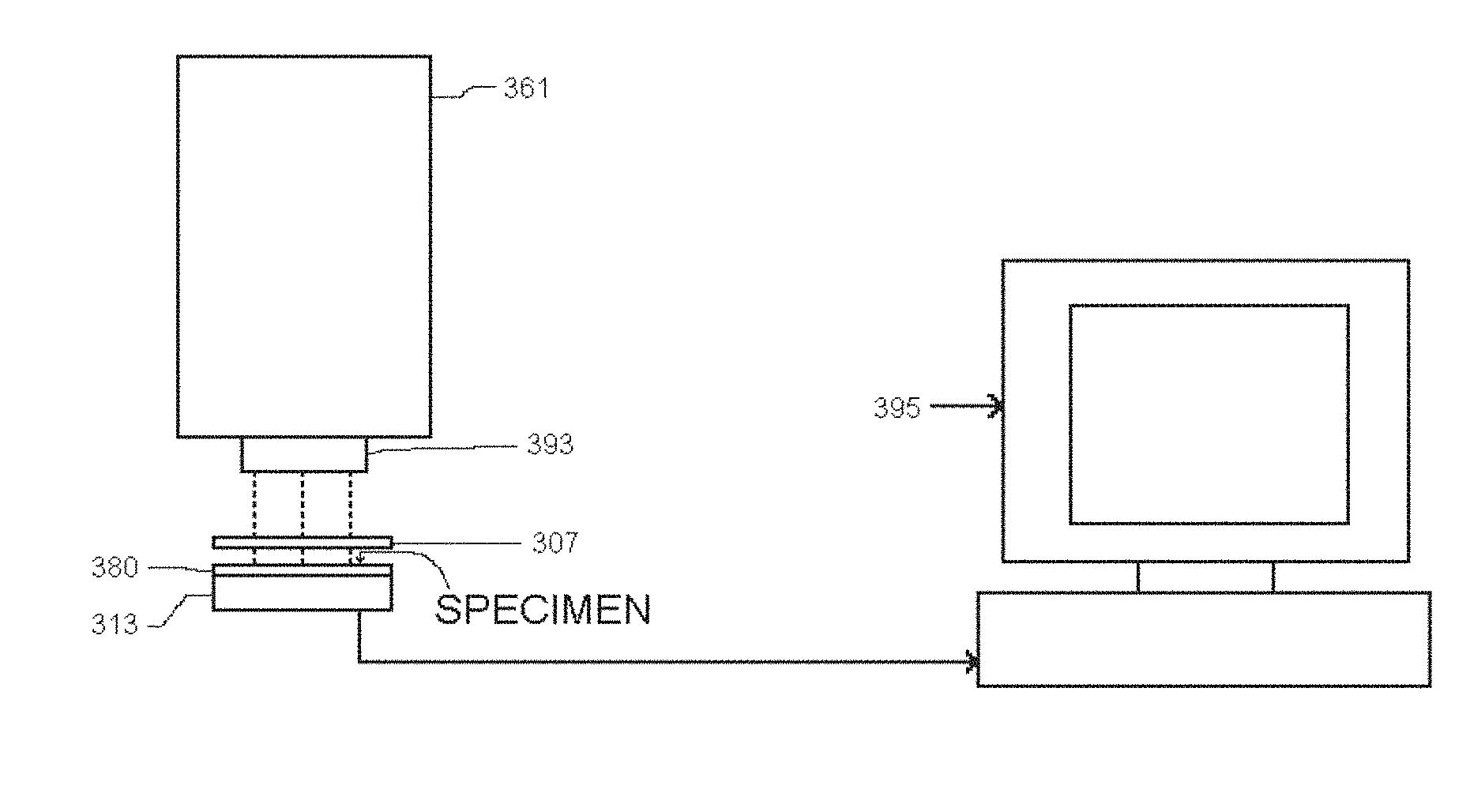
[0111] The spectra of the light source(s) may lie in any predetermined region of the electromagnetic spectrum detectable using photosensitive arrays, with or without specialized treatments to extend the effective ranges of wavelengths detectable by such arrays. In some embodiments, the predetermined wavelength or wavelength band is in the infrared spectrum. In some embodiments, the predetermined wavelength or wavelength band is in the ultraviolet spectrum. In some embodiments, the predetermined wavelength or wavelength band is in the visible spectrum. In some embodiments, the predetermined wavelength or wavelength band is in the X-ray spectrum. In some embodiments, the predetermined wavelength or wavelength band is in the microwave spectrum. In some embodiments, the predetermined wavelength or wavelength band is approximately that which has a frequency between about 1 Terahertz and about 1,000 Terahertz. Combinations of light in two or more bands may be used in some examples.
[0112] In some embodiments, the light source includes individually controlled light-emitting diodes (LEDs) selected for their spectral emission characteristics and their uniformity of emitted light, and positioned so as to facilitate the analyses contemplated. In some embodiments, the light sources are positioned so as to uniformly illuminate the specimen chamber. The LEDs are controlled, for example, by either an embedded controller incorporated within the instrument or by a microprocessor contained in smartphones or other commercially-available, "off-the-shelf" computing devices. The LEDs will be controlled, for example, either singly or in groups so as to facilitate the analyses to be contemplated, including but not limited to conventional microscopy wherein the illuminator, the specimen and the imaging system are substantially aligned, and dark-field microscopy wherein the specimen is illuminated from an angle outside the acceptance angle of the pixel. In addition, through appropriate selection of the LEDs in the illuminator, the contemplated contact microscope can be used for, but not be limited to, e.g., color imaging, fluorescence microscopy, polarization microscopy, infra-red and ultra-violet microscopy. Some embodiments will incorporate multiple illuminators, each of which may have different characteristics so as to facilitate the conduct of a wider range of analyses. In some embodiments the illuminators will be easily interchangeable. In some embodiments the illuminators may include organic LED (OLED) or active matrix organic LED (AMOLED) panel with selective addressing. Some embodiments facilitate both uniform specimen illumination and rapid illumination variation so as to facilitate analyses yet to be contemplated with both stationary and moving specimens. In some embodiments, an AMOLED panel may be used to illuminate the specimen through appropriate control of the panel photoemitters. In some examples, the illuminator can include LEDs, organic LED panels, fluorescent panels, x-ray sources, ultraviolet sources, ambient illumination such as sunlight or room light, incandescent sources, or any other light source, including none, e.g., for chemiluminescent specimens, and combinations of these examples. Configurations of the sources include, but are not limited to, flat panels, rectangular or other grid layouts of sources, movable sources, multi-color sources, and sources affixed to the inside or a hemispherical shell mounted over the specimen chamber with the centre of the chamber as the center of the shell, or combinations of them. Control of the illumination sources may include, but not be limited to, steady illumination, selectively exciting one or a plurality of illumination sources simultaneously or in sequence, controlling the intensity of any one or a plurality of sources, controlling each or a plurality of sources so as to have a specific temporal illumination pattern, or using any one or any combination of them and others (including future technologies). The controller for the illumination may include, but not be limited to, a manual controller such as a switch or knob, an automated embedded computing system, an external computing system such as a smartphone, an external computing system such as a desktop or laptop computer, or a combination of the foregoing. FIG. 7 illustrates features of some embodiments. In some examples, the imaging device 400 is placed in a housing 401 with a hinged lid, by which hinge dry specimens may be inserted and removed. On the underside of the lid, an organic LED light source 461 illuminates the specimen. Integral to the lid and bonded to the light source 461 is the circuitry 495 for input/output and illumination control. Power connector 458 is attached to the circuitry 495. Input/output connector 456, preferably a USB interface, is attached to the circuitry 495 adjacent to the light source 461. Paired fluid flow connectors 452, 454 attach to a fluid flow system akin to that in FIG. 4. The form factor of the entire embodiment of FIG. 7 can be about that of a smartphone, for example.
[0113] FIG. 8 illustrates the flow of light and output data when an embodiment of an imaging system is in operation. A light source 361 produces light in, for example, a predetermined wavelength or wavelength band. In some embodiments, a collimator 393 having a lens, filter, or combination thereof ensures that the light is collimated along an optical path and is composed of substantially only wavelengths of the predetermined wavelength or wavelength band. Light travels along the optical path toward the imaging integrated circuit 313. In some embodiments, the angle of incidence of the light onto the imaging integrated circuit will be oblique, rather than normal. In some embodiments, an optional cover 307 substantially transmissive to the predetermined wavelength or wavelength band restricts the specimen volume or protects the specimen from unintended movement or exposure. The specimen is illuminated, and the resultant light produces an image in the optical path beyond it. In some embodiments, an optional coating 380 lies between the specimen and the imaging integrated circuit 313. The resultant image as captured by the imaging integrated circuit 313 is outputted to a computer-based system 395 for storage, readout, or analysis.
[0114] In our discussion we use the term "high-resolution" to refer, for example, to a resolution that equals or exceeds the resolution of standard lens-based optical microscopes. For example, depending on the context of the application, high-resolution can mean less than 5 .mu.m, less than 2 .mu.m, less than 1 .mu.m, less than about 0.5 .mu.m, or even less. Resolution is primarily determined by the pixel size of the photosensitive array. Some photosensitive arrays have many million square pixels each slightly more than 1 .mu.m on a side, resulting in a resolution of about 1 .mu.m; the resolution achievable will improve with decreasing pixel sizes, theoretically exceeding, for example, 1 billion pixels, each as small as 200 nm or less on a side, as the design and fabrication techniques of integrated circuits or other devices improve. The number, shape, and arrangement of pixels in the array is arbitrary, with no intrinsic limit, and can be predetermined for manufacture based on the corresponding application of interest. In some embodiments, the longest pixel dimension is 10 .mu.m or smaller. In some embodiments, the longest pixel dimension is 5 .mu.m or smaller. In some embodiments, the longest pixel dimension is 1 micron or smaller. In some embodiments, the longest pixel dimension is 500 nm or smaller. In some embodiments, the longest pixel dimension is 250 nm or smaller.
[0115] Imaging integrated circuits can be constructed that have pixel sizes smaller than the wavelength of visible light, as shown, for example, in U.S. Pat. No. 7,153,720, incorporated here by reference. In some embodiments, the imaging integrated circuit includes a charge-coupled device (CCD). In other embodiments, the imaging integrated circuit is fabricated using complementary metal-oxide semiconductor (CMOS) technology. CCDs have advantages for contact optical microscopy applications, including the ability to detect light over the full exposed surface of the chip (100% fill factor), though they have slower readout speeds relative to CMOS due to requirement for sequential transfer of charge from light-sensing (parallel register) to readout (serial register) elements. Various configurations of CCD can be used: full-frame architecture is desirable to maximize the proportion of the chip available for imaging, but requires an external shutter to prevent image smearing during readout; whereas frame-transfer architecture avoids image smearing, but in the process requires a masked, non-photosensitive area of the parallel register of about the same size as the photosensitive area of the parallel register, with the result that the imaging integrated circuit has about half the photosensitive area of a full-frame architecture. Because of the small area of the individual pixels in the arrays used in this invention, the charge collected in each pixel will be small under many imaging conditions; however, as the specimen is in contact, or nearly in contact, with the pixel, the pixel's effective acceptance angle for photons emanating from the specimen is larger than that achieved by lenses in conventional microscopy. In some CCD embodiments, to increase the sensitivity further, CCDs of any architecture may additionally employ electron multiplying gain, in which high clock voltages applied to an extended region of the serial register(s) amplify the charge of each pixel as it is shifted to the output node(s).
[0116] CMOS devices have alternative advantages for these applications, including less expensive fabrication, signal processing by electronic elements embedded in individual pixels, and the ability to read out independently-addressed pixel values individually without sequential transfer. In some CMOS embodiments, thinned back-side illuminated arrays are used; though previously requiring expensive and complex fabrication methods, these can now be fabricated cheaply using bonded wafer processes such as those that use silicon-on-insulator substrates with a buried oxide layer as an etch-stop to yield a uniformly optimally thinned light-absorbing back layer (see as an example, U.S. Pat. No. 7,425,460, incorporated here by reference). Light entering ordinary (front-side illuminated) imaging integrated circuits typically passes through overlying layers that scatter light and whose metal circuit elements block the underlying photosensitive layer; in back-side illuminated imaging integrated circuits the photosensitive layer is close to the surface, above the metal circuit-bearing layers, typically resulting in less light blocking (larger "fill factors") and consequently higher effective quantum efficiency.
[0117] In some embodiments, the imaging integrated circuit is windowless. Most commercially available imaging devices have a protective window over the CCD or CMOS, and typically this window must be absent in order for the specimen to come close enough to the photosensitive surface to achieve high resolution, as defined above, without computational image processing. When a point on the specimen is less than half a pixel width from the center of the closest pixel, nearly all the light emitted or scattered from that point toward the array will predominantly be incident on, and therefore excite, only the closest pixel; under these conditions, resolution is determined by the pixel size or, more precisely, by the size of a circle of equivalent area (i.e., .about.450 nm resolution for a 400 nm.times.400 nm pixel), although resolution may be further enhanced by computation, specimen flow, or other means. No lenses or any other optical components are required to achieve these conditions, and thus to achieve such pixel-limited resolution.
[0118] Specimens or parts of specimens farther from the photosensitive surface are not imaged as sharply, due to the spread of light between the specimen and the photosensitive surface. As the distance between a point light source and the photosensitive surface of the array is increased, the image of the point at the photosensitive surface exhibits increasing blur, as light from the point impinges upon, and excites, additional pixels beyond the pixel directly below and nearest to the point. The extent of that spread to additional pixels is governed by two considerations that limit the angle of acceptance of light by the pixels (where angle of acceptance refers to the maximum deviation of a ray from the surface normal at which the ray can influence the pixel output).
[0119] Firstly, as the angle of incidence of light onto the photosensitive surface with respect to the surface normal is increased, an increasing portion of the light is reflected, until an angle is reached beyond which all the light is reflected. This relationship is defined by the Fresnel formulas as follows:
R s = [ n 1 cos .theta. i - n 2 1 - ( n 1 n 2 sin .theta. i ) 2 n 1 cos .theta. i + n 2 1 - ( n 1 n 2 sin .theta. i ) 2 ] 2 ##EQU00001## R p = [ n 1 1 - ( n 1 n 2 sin .theta. i ) 2 - n 2 cos .theta. i n 1 1 - ( n 1 n 2 sin .theta. i ) 2 + n 2 cos .theta. i ] 2 ##EQU00001.2##
where [0120] R.sub.s=reflection coefficient for s-polarized light [0121] R.sub.p=reflection coefficient for p-polarized light [0122] .theta..sub.i=angle of incident ray with respect to surface normal. [0123] n.sub.1=index of refraction for region containing light source [0124] n.sub.2=index of refraction for imaging array The transmission coefficients are:
[0124] T s = 1 - R s ##EQU00002## T p = 1 - R p ##EQU00002.2## T = T s + T p 2 ##EQU00002.3##
where T.sub.s is the resultant transmission coefficient for s-polarized light, T.sub.p is the resultant transmission coefficient for p-polarized light, and T is the resultant transmission coefficient for unpolarized light. The transmission coefficients are plotted in FIG. 10(a) for angles between zero and ninety degrees. From the figure it is seen that about 75 percent of unpolarized light is transmitted up to angles of about 60 degrees, after which point transmission falls off sharply.
[0125] Secondly, as the angle of light incidence with respect to the surface normal increases, the pixel poses a decreasing profile with respect to the light source.
[0126] This situation is shown in FIG. 10(b). In the figure, a point source of light 703 is positioned above the center of a pixel 713 that is part of a photosensitive array having pixels 701 that constitutes the photosensitive part of an imaging VLSI circuit 705. The center of the pixel 713 under the point light source 703 is the point of the photosensitive pixel array 701 closest to the point light source 703 and is denoted the origin 709 of the coordinate system used in the analysis. The light emitted from said point source is emitted in all directions equally. The light that falls on the pixel 713 immediately under said point light source receives an amount of light that is proportional to an angle 707 subtended by the area of the pixel at the said point light source. Similarly, the light received by any other pixel in the array, e.g., pixel 717, is proportional to an angle 711 that it subtends at the said point light source. For each pixel, the angle subtended at the point light source is a function of the pixel area projected toward the point light source and the distance from the point light source to said pixel.
[0127] The projection of the pixel area in the direction of the source is:
A p = mn d d 2 + r 2 ##EQU00003##
where d is the distance of the point source above the photosensitive surface, m and n are the x and y dimensions of each pixel respectively, and r is the distance from the point along the photosensitive surface to the pixel of interest. This projected area subtends a solid angle at the source given by:
.omega. = mnd ( d 2 + r 2 ) 3 / 2 ##EQU00004##
and so the proportion of the light flux emitted by the source that falls on this projected area is:
I i = I s mnd 4 .pi. ( d 2 + r 2 ) 3 / 2 ##EQU00005##
where I.sub.s is the source light flux and is the incident intensity on the projected area of the pixel under consideration. The light that passes into the pixel is this light, further attenuated by the transmission coefficient due to the angle made by the light with the surface of the pixel. Thus, the light available for detection is:
I p = T I s mnd 4 .pi. ( d 2 + r 2 ) 3 / 2 ##EQU00006##
[0128] For example, consider a specimen in aqueous suspension overlaying the surface of a photosensitive array constructed in silicon. Using an index of refraction n.sub.1 for water of 1.33 and for silicon n.sub.2 of 4.08, which are approximately their respective indices at a wavelength of 550 nm, the computed spread of detected intensity of light emitted by a point source as a function of distance of the source from the silicon surface is shown in FIG. 9. Standard algorithms for image sharpening can utilize this data for improvement of image quality.
[0129] Tolerance for such blurring will depend upon the specific imaging application; in some cases, useful information can be obtained from specimen regions that do not satisfy the near-field criterion, such as specimens many micrometers or tens of micrometers from the photosensitive surface. In some embodiments, the distance between the specimen and the photosensitive surface is approximately equal to one of the following quantities: ten times the average wavelength produced by the light source, or less than five times the average wavelength, or preferably less than three times the average wavelength, or more preferably less than the predetermined wavelength, or still more preferably less than half the predetermined wavelength.
[0130] In some embodiments, some of the supporting circuitry for readout is contained within the imaging integrated circuit. In some embodiments, the supporting circuitry is coupled to additional supporting circuitry or microprocessors that control the functions of the integrated circuit, such as gain or data clock rate. In some embodiments, the imaging integrated circuit is commercial and off-the-shelf, having a high-resolution photosensitive array, supporting circuitry for readout, and an industry-standard interface for connection to a computer-based system for image data display, storage, and analysis, for example, the Aptina MT9E013, the OmniVision OV14825, and the OmniVision OV14810; the technical data for which are incorporated here by reference. As an illustrative example, the OmniVision OV5642 incorporates the full functionality of a single chip, 5 megapixel digital camera with 1.4 micron pixel widths, including output of images at 15 frames per second (fps) in RAW RGB mode and up to 60 fps in 1080i resolution. The OV5642 supplies images for readout via serial camera control bus (SCCB) and mobile industry processor (MIPI) interfaces using digital video parallel and MIPI serial ports. It also supports output in RGB565/855/444, CCIR656, W1/422/420, and YCbCr422 modes. The signal descriptions, pad numbers, and corresponding block and pad diagrams for OV5642 illustrate a preferred implementation for an imaging integrated circuit; these are hereby incorporated by reference to the OmniVision OV5642 datasheet and product specification version 2.03. Computer-based systems that are capable of connection to the supporting circuitry may be embedded or standalone, purpose-built or off-the-shelf, including, for example purpose-designed embedded computing systems, smartphones, portable computers, and netbooks.
[0131] In some embodiments, the computer-based system has firmware or software for image analysis, storage, illumination control, and display. Such firmware or software has previously been paired with optical microscopes and digital camera technology. In some embodiments, the computer-based system implements algorithms to enhance, detect, analyze, characterize, and measure images of cells and other specimens of interest and to display or transmit the result of these algorithms to a human operator and/or a second computer-based system, such as a smartphone or storage system including hospital record storage systems. In some embodiments, the computer-based system implements enhancement algorithms that can identify ages of discrete specimens in smooth flow in a series of time-lapsed images.
[0132] In some embodiments, the imaging integrated circuit's supporting circuitry is coupled to additional circuitry on the mounting block. In some embodiments, the mounting block incorporates certain interfaces in hardware that are capable of supplying the RAW, RGB, and/or TWAIN standard. Examples of interfaces for optical microscope cameras that could be adapted include those included in the Jenoptik ProgRes Professional Color CCD Firewire Camera; the Luminera Infinity Color CCD or CMOS USB-2 Cameras; and the Motic Moticam Color CMOS USB-2 Camera; the technical data and owner's manuals for which are incorporated here by reference. In some embodiments, a computer-based system is coupled to the mounting block interfaces for imaging analysis, display, and storage. Examples of imaging analysis software that could be used include ProgRes CapturePro, Infinity Capture and Infinity Analyze, and Motic Images Plus; the technical data and owner's manuals for which are incorporated here by reference. In some embodiments, the image captured by the imaging integrated circuit is outputted to a storage medium. In some embodiments, the image captured by the imaging integrated circuit is outputted to a real-time display device. In some embodiments, only pixels of interest need be output from the imaging integrated circuit in order to maintain a desired high temporal resolution; CMOS-based imaging integrated circuits are well suited for this task but other architectures are possible. The raw data of pixel array intensities, or the post-acquisition images themselves, may be enhanced by various computational means including but not limited to deconvolution, pixel interpolation, spatial filtering, noise reduction, edge enhancement, and other methods.
[0133] Moreover, in some embodiments, a suboptimal point-spread function (whereby light meant to be detected at a given pixel is also detected by an adjacent pixel) may be corrected computationally. In some embodiments of an imaging system, the imaging integrated circuit, associated electronics, and analysis device are integrated so as to be combined in a portable housing; the light source may be integrated, standalone, or supplied from ambient light, allowing for desktop-, laptop-, cellphone-, or smaller-sized microscopes as the desired application requires.
[0134] In some embodiments, there is a chamber lid that is substantially transmissive to at least one wavelength of light produced by a light source. The locating block is preferably a rectangle. The walls of the chamber lid may be square, rectangular, circular, elliptical, or some other shape appropriate to the specimen being imaged. In some embodiments, the top surface of the chamber lid is absent and a multi-colour light-emitting display surface forms the top of the specimen chamber. In some embodiments, the chamber lid and locator block are partially or substantially transparent or translucent. In other embodiments, the chamber lid and locator block are opaque; examples of applications for such a design include chemiluminescence imaging and autoradiography. In some embodiments, the specimen chamber lid is not present, as for microscopic imaging of the surface of large or thick specimens.
[0135] In some embodiments, the specimen chamber has a probe; examples of probes include temperature probe 501 and pH probe 503. In some embodiments, the specimen chamber has a pair or more of mounted electrodes 507, 509 along the perimeter of the chamber for applying transverse or longitudinal electric fields or for stimulation of specimens. Such an arrangement of electrodes may be used, as examples and in conjunction with appropriate fluid handling as described above, for electrophoresis, separation/sorting, determination of specimen surface charge, determination of zeta potential, cell stimulation, and specimen orientation. In some embodiments, the specimen chamber has a heating element 505. Such a heating element may be used, as examples, in the observation of time-dependent processes and in the incubation of live specimens for time-lapse imaging.
[0136] In some embodiments, the photosensitive surface has been treated with one or more thin layers. The layers may be considered thin when the aggregate thickness of such layers as applied to a photosensitive surface still allows for the near-field criterion to be satisfied or approximately satisfied. In some embodiments, the layers are thin enough for specimens to come within half a pixel width of the photosensitive surface. In some embodiments, the layers are thin enough in the direction of the optical path so that the total distance that the optical path takes through the layers is no more than about the wavelength of interest. In some embodiments, a thin layer of transparent chemically resistant material coats the photosensitive surface. Such a thin-film substrate may be any sufficiently transparent and insulating material, including but not limited to silicon oxide, titanium oxide, aluminum oxide, tantalum oxide, magnesium fluoride, lanthanum fluoride, aluminum fluoride, silicon nitride, and silicon oxynitride; and it may be deposited by a variety of means including but not limited to magnetron sputtering, chemical vapour deposition, thermal or vacuum arc plasma evaporation. In some embodiments, the substrate is a dielectric thin film acting as an interference filter, thereby restricting the spectral sensitivity of the underlying pixels as appropriate to a given application. In some embodiments, the substrate is used to effect certain forms of color imaging. In certain embodiments, the substrate is substantially transmissive to a portion of a predetermined wavelength band, such as a band-pass filter. In other embodiments such as for fluorescence or emission microscopy, the substrate 618 is substantially transmissive to an alternative predetermined wavelength band which corresponds to the wavelength band produced by fluorescence, emission, or in other ways, of the specimen. In some embodiments, the substrate includes a dielectric thin film acting as an anti-reflection coating. In some embodiments, there are multiple substrates situated in close contact to each other. In some embodiments, the photosensitive surface is silanized so as to decrease adhesion between the surface and the specimen. In some embodiments, the chemically resistant material 615 includes diamond, deposited in a suitably thin layer as, for example, by chemical vapor deposition. In some embodiments, the chemically resistant material includes Al.sub.2O.sub.3 or Si.sub.3N.sub.4, deposited in a suitably thin layer as, for example, by chemical vapour deposition. Such materials can impart more robust characteristics to the photosensitive surface, allowing for ease of cleaning as well as protection of the surface from abrasive specimens. In some embodiments, a passivation layer 620, typically of Si.sub.3N.sub.4, coats the imaging integrated circuit, resulting in reduced conductivity when used with metallic or other conductive samples such as salt solutions. Technology is available to deposit such filters as a thin film and in arbitrary pixel-by-pixel patterns.
[0137] In some embodiments, a thin layer of polarizing material 614 coats the photosensitive surface. In some embodiments, a thin layer of absorptive material 614 coats the photosensitive surface. In some embodiments, a thin layer of interference material 614 coats the photosensitive surface. In some embodiments, a thin layer of surface plasmon generating material 619 coats the photosensitive surface.
[0138] In some embodiments, a thin layer of adhesive material 617 coats the imaging integrated circuit 613. Coatings with molecules having specific affinities can be used to exclude or enrich particular cells or other specimens of interest. Such treatment could also be used, in conjunction with fluorophores 616, nanoparticles or microbeads, for binding assays. Non-selective adhesives will create an imaging "stick patch" that could be used, as an example, for forensic applications. In some embodiments, a thin layer of light-transmissive material 614 containing fluorophores, phosphors or up-converters coats the photosensitive surface. Such molecules are excited at one wavelength and emit at another. In some embodiments, fluorophores are excited with wavelengths outside the spectrally sensitive range of the imaging integrated circuit and emitting, including by frequency upconversion, within the circuit's spectral range, thereby extending the useful spectral range of the imaging integrated circuit, e.g. into the X-ray spectrum. In some embodiments, the device further comprises a system for detecting Raman scattering. In some embodiments, the device further comprises a system for detecting X-ray fluorescence.
Example 1
[0139] A specimen of a thin Mylar sheet was placed in direct contact with the exposed surface of a commercially available, 1.3 megapixel CMOS imaging integrated circuit having 5.2 .mu.m.times.5.2 .mu.m pixels, and an image (FIG. 11) was collected using a diffuse white light source, a computer, and commercially available image acquisition software. The upper left and upper right corners of the field of view are empty, with the specimen filling the rest of the field of view; scratches and other features of the specimen as small as single pixels are clearly visible.
Example 2
[0140] Using the CMOS imaging integrated circuit and light source of Example 1, a specimen of aerosol organic solvent was nebulized and thereby deposited onto the chip surface. Acquisition of the image produced FIG. 12.
Example 3
[0141] A 1 .mu.l droplet of water was deposited directly onto the CMOS chip surface as in Examples 1 and 2, using the same light source. Edges of the droplet spontaneously aligned with the pixel rows and columns, yielding the unusual lozenge shape. Suspended in the droplet were Sephadex beads of sizes ranging from <20 .mu.m to >100 .mu.m. Acquisition of the image produced FIG. 13. The larger beads cast a prominent diffuse shadow because their equators are far from the surface. This effect would be slightly reduced with collimated illumination and is much reduced with smaller beads.
Example 4
[0142] The protective window of an Aptina CMOS imaging integrated circuit was removed, exposing the photosensitive surface of the array having of 2.2 .mu.m.times.2.2 .mu.m pixels. A diffuse white light source was used, as was a computer-based system equipped with commercially available software for image acquisition as supplied with the array. A minute sample (.about.10 .mu.l) of blood was obtained from an African clawed frog (Xenopus laevis) and diluted in calcium-free amphibian Ringer's solution. A drop of the diluted blood was deposited directly onto the surface of the array. Acquisition of an image by the array produced FIG. 14 (top); a small portion of this large (3.2.times.2.4 mm) field of view can be seen-at higher magnification simply by "zooming in" on the acquired image (FIG. 9, bottom). The elliptical shape and nucleated structure of these living, unstained erythrocytes (long axis .about.24 .mu.m, short axis .about.16 .mu.m) is clearly evident. The zoomed image was enhanced by 2.times.2 pixel augmentation with bicubic interpolation. The images produced were intrinsically calibrated, as the dimensions of the pixels are known. In this Example, pixels are 2.2 .mu.m wide in the raw image, and 1.1 .mu.m wide in the 2.times.2 interpolated image.
Example 5
[0143] Using the same imaging integrated circuit of Example 4, a video sequence of a live Daphnia in pond water was obtained, a region of interest from two frames of which is shown in FIG. 15.
[0144] Other embodiments are also within the scope of the following claims.
* * * * *
D00000
D00001
D00002
D00003
D00004
D00005
D00006
D00007
D00008
D00009
D00010
D00011
D00012

D00013
D00014

D00015


XML
uspto.report is an independent third-party trademark research tool that is not affiliated, endorsed, or sponsored by the United States Patent and Trademark Office (USPTO) or any other governmental organization. The information provided by uspto.report is based on publicly available data at the time of writing and is intended for informational purposes only.
While we strive to provide accurate and up-to-date information, we do not guarantee the accuracy, completeness, reliability, or suitability of the information displayed on this site. The use of this site is at your own risk. Any reliance you place on such information is therefore strictly at your own risk.
All official trademark data, including owner information, should be verified by visiting the official USPTO website at www.uspto.gov. This site is not intended to replace professional legal advice and should not be used as a substitute for consulting with a legal professional who is knowledgeable about trademark law.