Method Of Sequential Infiltration Synthesis Treatment Of Infiltrateable Material And Structures And Devices Formed Using Same
Kachel; Krzysztof ; et al.
U.S. patent application number 16/137974 was filed with the patent office on 2019-03-21 for method of sequential infiltration synthesis treatment of infiltrateable material and structures and devices formed using same. The applicant listed for this patent is ASM IP Holding B.V.. Invention is credited to David de Roest, Krzysztof Kachel.
| Application Number | 20190086807 16/137974 |
| Document ID | / |
| Family ID | 65720212 |
| Filed Date | 2019-03-21 |
| United States Patent Application | 20190086807 |
| Kind Code | A1 |
| Kachel; Krzysztof ; et al. | March 21, 2019 |
METHOD OF SEQUENTIAL INFILTRATION SYNTHESIS TREATMENT OF INFILTRATEABLE MATERIAL AND STRUCTURES AND DEVICES FORMED USING SAME
Abstract
The disclosure relates to a sequential infiltration synthesis for treatment of infiltrateable material.
| Inventors: | Kachel; Krzysztof; (Chandler, AZ) ; de Roest; David; (Kessel-Lo, BE) | ||||||||||
| Applicant: |
|
||||||||||
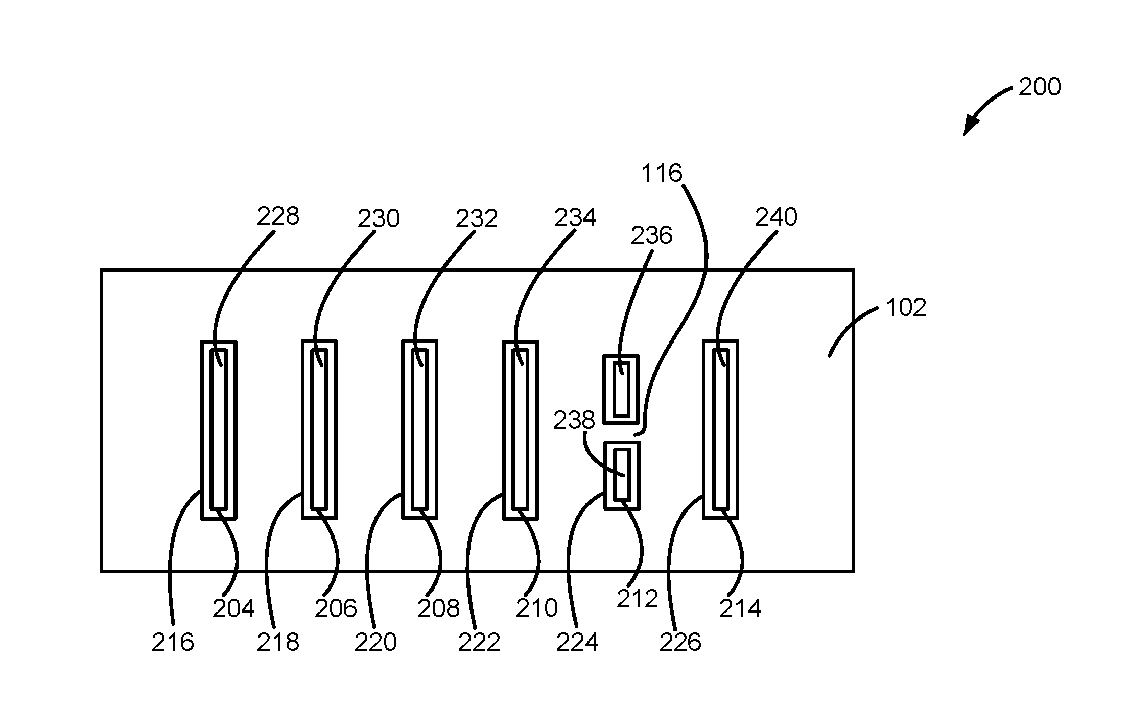
|---|---|---|---|---|---|---|---|---|---|---|---|
| Family ID: | 65720212 | ||||||||||
| Appl. No.: | 16/137974 | ||||||||||
| Filed: | September 21, 2018 |
Related U.S. Patent Documents
| Application Number | Filing Date | Patent Number | ||
|---|---|---|---|---|
| 62561600 | Sep 21, 2017 | |||
| Current U.S. Class: | 1/1 |
| Current CPC Class: | G03F 7/405 20130101; C23C 16/45525 20130101; C23C 16/45553 20130101; C23C 16/045 20130101; C23C 16/40 20130101; G03F 1/72 20130101; G03F 7/167 20130101 |
| International Class: | G03F 7/16 20060101 G03F007/16; C23C 16/455 20060101 C23C016/455 |
Claims
1. A method of forming a structure on a substrate comprising: providing the substrate with a infiltrateable material in a reaction chamber; and infiltrating the infiltrateable material with infiltration material during one or more infiltration cycles comprising: a) providing a first precursor to the infiltrateable material on the substrate in the reaction chamber, b) removing a portion of the first precursor for a second period from the reaction chamber; and, c) providing a second precursor to the infiltrateable material on the substrate for a third period, allowing the first and second precursor to react with each other forming the infiltration material in the infiltrateable material.
2. The method of claim 1, wherein the infiltrateable material comprises photoresist material.
3. The method of claim 1, wherein the infiltrateable material comprises features and at least one of the features comprises a defect.
4. The method of claim 3, wherein the structure comprises a layer comprising the infiltration material formed over and/or in place of the defect.
5. The method of claim 1, wherein the infiltrateable material is or comprises EUV photoresist.
6. The method of claim 1, wherein the defect is or comprises line breakage.
7. The method of claim 6, wherein the line breakage defect is repaired by the infiltration material formed on the surface of the infiltrateable material.
8. The method of claim 1, wherein the infiltrateable material is structured to have a defined, non-continuous pattern over the substrate.
9. The method of claim 1, wherein the infiltrateable material is or comprises a line of photoresist.
10. The method of claim 1, wherein the infiltrateable material is or comprises patterned photoresist.
11. The method of claim 6, wherein the line breakage defect is repaired by the infiltration material formed on the surface of the photoresist, so that infiltration material from both sides of the defect touches each other.
12. The method of claim 6, wherein the line breakage defect is repaired by the infiltration material formed on the surface of the photoresist so that infiltration material width over the defect is at least 25% of width of the photoresist line without defect.
13. The method of claim 6, wherein the line breakage defect is repaired by the infiltration material formed on the surface of the photoresist so that infiltration material width over the defect is at least 50% of width of the photoresist line without defect.
14. The method of claim 6, wherein the line breakage defect is repaired by the infiltration material formed on the surface of the photoresist so that infiltration material width over the defect is at least 75% of width of the photoresist line without defect.
15. The method of claim 1, wherein the first precursor comprises one of TMA and H.sub.2O.
16. The method of claim 1, wherein the second precursor comprises one of TMA and H.sub.2O.
17. The method of claim 1, wherein during the step of infiltrating a temperature within a reaction chamber is 150.degree. C., below 120.degree. C. or below 100.degree. C.
18. The method of claim 1, wherein a number of cycles is greater than 1, or between about 2 and about 10.
19. The method of claim 1, wherein a thickness of a layer formed during the step of providing a second precursor is from about 0.1 nm to about 50 nm, about 0.5 nm to about 30, or about 1 nm to about 20 nm.
20. A structure formed using the method of claim 1.
21. A device formed using the method of claim 1.
22. A device formed using the structure of claim 20.
Description
CROSS-REFERENCE TO RELATED APPLICATION
[0001] This application claims the benefit of U.S. Provisional Application No. 62/561,600, entitled "METHOD OF SEQUENTIAL INFILTRATION SYNTHESIS TREATMENT OF INFILTRATEABLE MATERIAL AND STRUCTURES AND DEVICES FORMED USING SAME" and filed on Sep. 21, 2017, the disclosure of which is hereby incorporated herein for reference.
FIELD OF INVENTION
[0002] The present disclosure generally relates to methods to manufacture electronic devices. More particularly, the disclosure relates to methods of forming a structure on a substrate using a sequential infiltration synthesis treatment of infiltrateable material, such as photoresist, and to structures and devices formed using such methods.
BACKGROUND
[0003] As the trend has pushed semiconductor devices to smaller and smaller sizes, different patterning techniques have arisen. These techniques include spacer defined quadruple patterning, extreme ultraviolet lithography (EUV), and EUV combined with spacer defined double patterning. In addition, directed self-assembly (DSA) has been considered as an option for future lithography applications. DSA involves the use of block copolymers to define patterns for self-assembly. The block copolymers used may include poly(methyl methacrylate) (PMMA), polystyrene, or poly(styrene-block-methyl methacrylate) (PS-b-PMMA). Other block copolymers may include emerging "high-Chi" polymers, which may potentially enable small dimensions.
[0004] The patterning techniques described above may utilize an infiltrateable material, such as an EUV polymer or DSA block copolymer resist, disposed on a substrate to enable high resolution patterning of the substrate. To satisfy the requirements of both high resolution and line-edge roughness, the polymer resist may commonly be a thin layer. However, such thin polymer resists layer may have several drawbacks. In particular, high resolution polymer resists may have low etch resistance and may suffer from voids or gaps in a photoresist pattern, which can affect a pattern that is transferred using the photoresist or other infiltrateable material. If such defects are detected during inspection, a substrate is often reworked, which adds time and cost to device manufacturing.
[0005] Improved methods for forming and transferring patterns using infiltrateable material, such as photoresist, are therefore desired.
SUMMARY
[0006] Various embodiments of the present disclosure relate to methods of forming structures using sequential infiltration synthesis treatment of infiltrateable material, such as photoresist, and to structures and devices formed using such methods. As set forth in more detail below, exemplary methods can be used to treat infiltrateable material, such that line breakages and/or gap formation that may occur during a pattern transfer process, can be repaired. As a result, the methods described below may result in less reworking of substrates.
[0007] In accordance with at least one embodiment of the disclosure, a method of forming a structure on a substrate includes providing the substrate with (e.g., patterned) infiltrateable material (e.g., a photoresist material) in a reaction chamber and infiltrating the infiltrateable material with infiltration material during one or more infiltration cycles. Each infiltration cycle can include: a) providing a first precursor to the infiltrateable material on the substrate in the reaction chamber, b) removing a portion of the first precursor for a second period from the reaction chamber, and c) providing a second precursor to the infiltrateable material on the substrate for a third period, allowing the first and second precursor to react with each other to thereby form the infiltration material in the infiltrateable material. The infiltrateable material may have one or more defects. The infiltration material can be formed on the surface of the infiltrateable material, such that the infiltration material on the surface of the infiltrateable material forms over any defects (e.g., gaps or line breakages) in the infiltrateable material. By way of examples, the infiltrateable material can include or be EUV photoresist. The infiltrateable material can include patterns that include defined, non-continuous features over the substrate, such as one or more lines of infiltrateable material. As discussed in more detail below, in accordance with various aspects of these embodiments, a defect (e.g., line defect) in infiltrateable material can be repaired using the methods described herein. For example, a layer including the infiltration material can form at a top surface of patterned infiltrateable material (e.g., in the form of lines) to mitigate pattern transfer problems and/or to repair the infiltrateable material. An infiltration material width over a defect can be at least 25%, 50%, or 75% of a width of the infiltrateable material line without the defect (e.g., a width of an infiltrateable feature width prior to treatment with or exposure to infiltration material). The infiltration step can include, for example, using TMA and H.sub.2O as first and second precursors (in any order) at a temperature--e.g., a temperature sufficient to cause the desired reactions (e.g., about room temperature or about 20.degree. C.) and/or below 150.degree. C., below 120.degree. C. or below 100.degree. C. and/or at a pressure of about 9 Torr to about 750 or about 760 Torr. A number of infiltration cycles can include, for example, greater than 1, about 2 to about 10, or about 5 cycles.
[0008] For purposes of summarizing the invention and the advantages achieved over the prior art, certain objects and advantages of the invention have been described herein above. Of course, it is to be understood that not necessarily all such objects or advantages may be achieved in accordance with any particular embodiment of the invention. Thus, for example, those skilled in the art will recognize that the invention may be embodied or carried out in a manner that achieves or optimizes one advantage or group of advantages as taught or suggested herein without necessarily achieving other objects or advantages as may be taught or suggested herein.
[0009] All of these embodiments are intended to be within the scope of the invention herein disclosed. These and other embodiments will become readily apparent to those skilled in the art from the following detailed description of certain embodiments having reference to the attached figures, the invention not being limited to any particular embodiment(s) disclosed.
BRIEF DESCRIPTION OF THE FIGURES
[0010] A more complete understanding of exemplary embodiments of the present disclosure can be derived by referring to the detailed description and claims when considered in connection with the following illustrative figures.
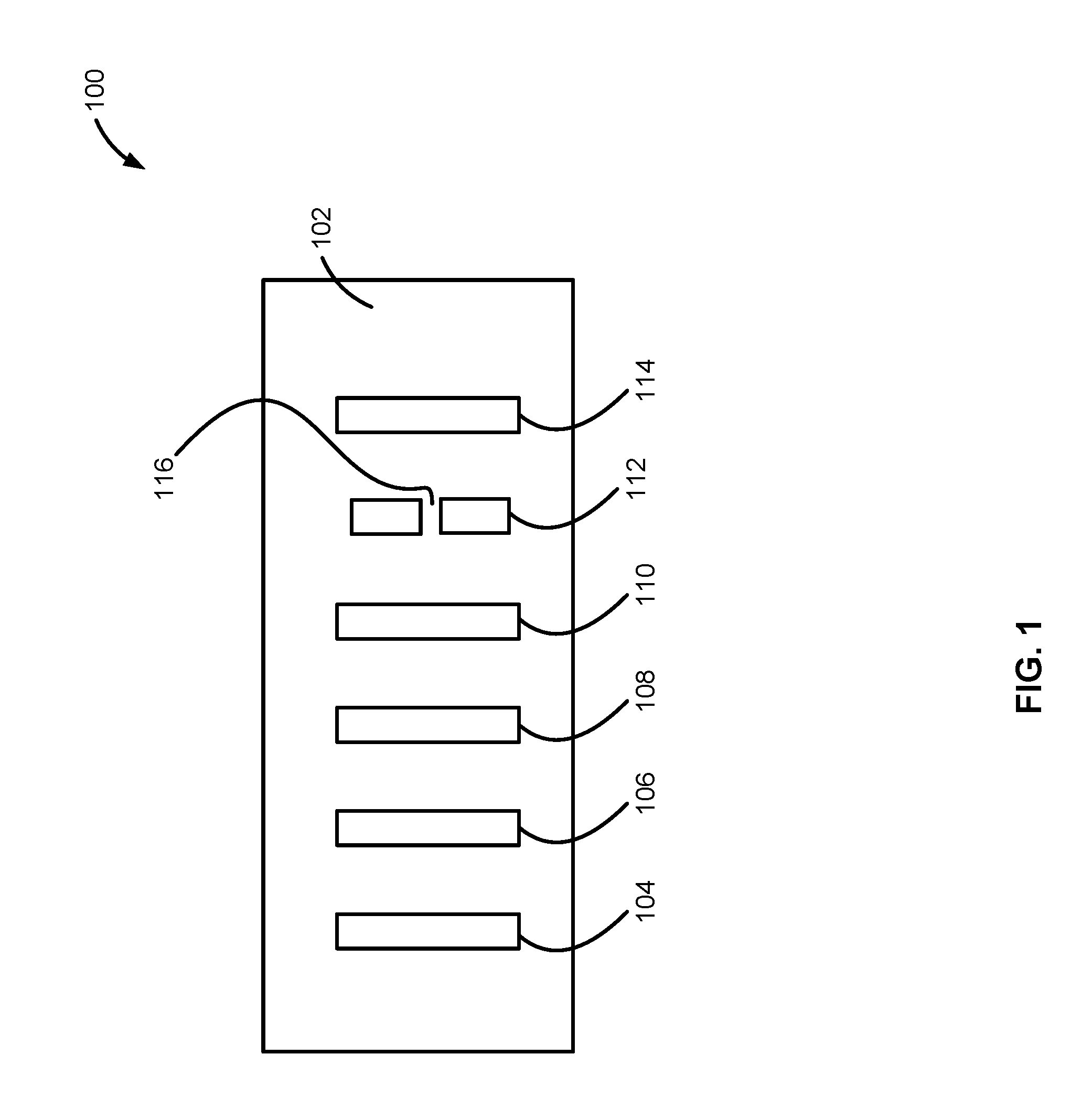
[0011] FIG. 1 illustrates patterned infiltrateable material features, wherein one of the features includes a defect.
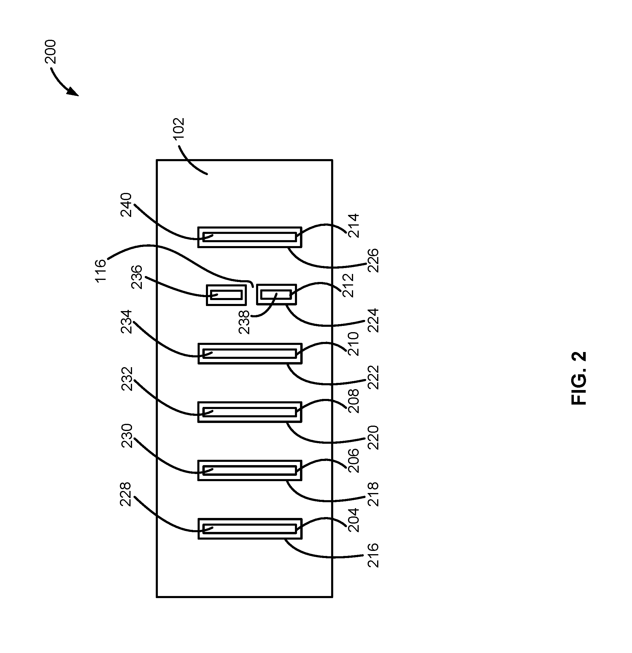
[0012] FIG. 2 illustrates the patterned infiltrateable features of FIG. 1 after treatment in accordance with at least one embodiment of the disclosure.
[0013] It will be appreciated that elements in the figures are illustrated for simplicity and clarity and have not necessarily been drawn to scale. For example, the dimensions of some of the elements in the figures may be exaggerated relative to other elements to help to improve the understanding of illustrated embodiments of the present disclosure.
DETAILED DESCRIPTION
[0014] Although certain embodiments and examples are disclosed below, it will be understood by those in the art that the invention extends beyond the specifically disclosed embodiments and/or uses of the embodiments and obvious modifications and equivalents thereof. Thus, it is intended that the scope of the invention disclosed should not be limited by the particular disclosed embodiments described below.
[0015] As noted above, the present disclosure relates to methods of forming structures using sequential infiltration synthesis treatment of infiltrateable material, such as photoresist, and to structures and devices formed using such methods. Exemplary apparatus suitable for such treatment are disclosed in U.S. patent application, entitled "SEQUENTIAL INFILTRATION SYNTHESIS APPARATUS," filed Dec. 15, 2016, and assigned Ser. No. 15/380,909, the contents of which, to the extend such contents do not conflict with the present disclosure, are hereby incorporated herein by reference.
[0016] FIG. 1 illustrates a structure 100 including a substrate 102 and patterned features (e.g., lines) of infiltrateable materials 104-114 formed thereon. Features 104-114 can be formed of, for example, photoresist material, such as EUV photoresist or the like. As illustrated in FIG. 1, features 104-114 can be defined, non-continuous features. As further illustrated, at least one of the features, feature 112 in the illustrated example, includes a defect 116, such as a (line) breakage or a gap. With typical process, if defect 116 was detected during an inspection, substrate 102 would be discarded or reworked.
[0017] FIG. 2 illustrates a structure 200 after a treatment, in accordance with at least one embodiment of the disclosure. Structure 200 includes features 204-214 that include layers 216-226 that include infiltration material. Features 204-214 can also include portions 228-240 that do not include or that include relatively small amounts of infiltration material. Layer 224 that is formed over defect 116 can be about or at least 25%, 50%, or 75% of width of the infiltrateable material line (e.g., one of lines 104-110, 114) without defect. As further illustrated, layer 224 can be continuous in the location of defect 116. In other words, layer 224 can grow from features 112 to touch, and thereby "repair" the feature. Accordingly, when a defect is detected, the substrate need not be discarded or reworked. Features including layer 216-226 can have dimensions (e.g., width, height, and/or length) that are larger than the original features (e.g., features 104-114).
[0018] A method of forming a structure (e.g., structure 200) on a substrate in accordance with at least one embodiment of the disclosure includes providing a substrate (e.g., substrate 102) with (e.g., patterned) infiltrateable material (e.g., a photoresist material) in a reaction chamber and infiltrating the infiltrateable material with infiltration material during one or more infiltration cycles. Each infiltration cycle can include: a) providing a first precursor to the infiltrateable material on the substrate in the reaction chamber, b) removing a portion of the first precursor for a second period from the reaction chamber, and c) providing a second precursor to the infiltrateable material on the substrate for a third period, allowing the first and second precursor to react with each other forming the infiltration material in the infiltrateable material.
[0019] An interaction of a precursor, e.g., TMA, with the infiltrateable material may be primarily through adsorption and diffusion. The temperature may have a significant effect on the infiltration because the rate of adsorption and diffusion and the equilibrium in an adsorption reaction may be impacted by changes in temperature. In accordance with exemplary embodiments, a temperature within a reaction chamber during a treatment can be 150.degree. C., below 120.degree. C. or below 100.degree. C. and/or about ambient temperature of about 20.degree. C.
[0020] During treatment, the first precursor can be infiltrated in the infiltrateable material on the substrate by exposure to the first precursor in vapor phase from a container. The first precursor can react with the infiltrateable material on the substrate and become a chemi-sorbed or physi-sorbed derivative infiltrated in the infiltrateable material on the substrate, and can thereby form a layer including the infiltration materials. Subsequently the second precursor can infiltrated in the infiltrateable material on the substrate by exposure to the second precursor in vapor phase from a container. The second precursor can react with the chemi-sorbed or physi-sorbed derivative of the first precursor infiltrated in the infiltrateable material on the substrate to become the final infiltration material. During this process, a layer including the infiltration material can grow, causing the features to swell, to thereby repair any defects in features.
[0021] The first or second precursor can be a metal precursor, such as a compound of aluminum selected from the group consisting of trimethyl aluminum (TMA), triethyl aluminum (TEA), and dimethylaluminumhydride (DMAH). The other of the first and second precursor can be, for example, an oxidant or oxygen precursor, such as water. The first precursor and the second precursor may be utilized to infiltrate the infiltrateable material with one or more of aluminum oxide (Al2O3), silicon oxide, (SiO2), silicon nitride (SiN), silicon oxynitride (SiON), silicon carbonitride (SiCN), silicon carbide (SiC), titanium carbide (TiC), aluminum nitride (AlN), titanium nitride (TiN), tantalum nitride (TaN), tungsten (W), cobalt (Co), titanium oxide (TiO2), tantalum oxide (Ta2O5), zirconium oxide (ZrO2), or hafnium oxide (HfO2).
[0022] A number of cycles performed can be more than one, about 2 to about 10, or be about 5. A layer, such as layer 216, can be from about 0.1 nm to about 50 nm, about 0.5 nm to about 30, or about 1 nm to about 20 nm.
* * * * *
D00000
D00001
D00002
XML
uspto.report is an independent third-party trademark research tool that is not affiliated, endorsed, or sponsored by the United States Patent and Trademark Office (USPTO) or any other governmental organization. The information provided by uspto.report is based on publicly available data at the time of writing and is intended for informational purposes only.
While we strive to provide accurate and up-to-date information, we do not guarantee the accuracy, completeness, reliability, or suitability of the information displayed on this site. The use of this site is at your own risk. Any reliance you place on such information is therefore strictly at your own risk.
All official trademark data, including owner information, should be verified by visiting the official USPTO website at www.uspto.gov. This site is not intended to replace professional legal advice and should not be used as a substitute for consulting with a legal professional who is knowledgeable about trademark law.