Optoelectronic Modules With Alignment Spacers and Methods for Assembling the Same
Balimann; Martin Lukas ; et al.
U.S. patent application number 16/093840 was filed with the patent office on 2019-03-14 for optoelectronic modules with alignment spacers and methods for assembling the same. The applicant listed for this patent is Heptagon Micro Optics Pte. Ltd.. Invention is credited to Martin Lukas Balimann, Matthias Gloor, Hartmut Rudmann, Nicola Spring.
| Application Number | 20190081187 16/093840 |
| Document ID | / |
| Family ID | 60042062 |
| Filed Date | 2019-03-14 |


| United States Patent Application | 20190081187 |
| Kind Code | A1 |
| Balimann; Martin Lukas ; et al. | March 14, 2019 |
Optoelectronic Modules With Alignment Spacers and Methods for Assembling the Same
Abstract
Optoelectronic modules, such as proximity sensors, two-dimensional and three-dimensional cameras, structured- or encoded-light emitters, and projectors include optical assemblies and active optoelectronic components that are light sensitive or emit light. The optical assemblies are aligned to the active optoelectronic components via alignment spacers and adhesive. The alignment spacers include surfaces operable to limit the lateral migration of adhesive thereby preventing the contamination of the active optoelectronic components with adhesive. In some instances, small optoelectronic module footprints can be maintained without compromising the integrity of the adhesive.
| Inventors: | Balimann; Martin Lukas; (Zurich, CH) ; Gloor; Matthias; (Boswil, CH) ; Rudmann; Hartmut; (Jona, CH) ; Spring; Nicola; (Wangen, CH) | ||||||||||
| Applicant: |
|
||||||||||
|---|---|---|---|---|---|---|---|---|---|---|---|
| Family ID: | 60042062 | ||||||||||
| Appl. No.: | 16/093840 | ||||||||||
| Filed: | April 11, 2017 | ||||||||||
| PCT Filed: | April 11, 2017 | ||||||||||
| PCT NO: | PCT/SG2017/050204 | ||||||||||
| 371 Date: | October 15, 2018 |
Related U.S. Patent Documents
| Application Number | Filing Date | Patent Number | ||
|---|---|---|---|---|
| 62322966 | Apr 15, 2016 | |||
| Current U.S. Class: | 1/1 |
| Current CPC Class: | G03B 17/12 20130101; G02B 19/0047 20130101; G02B 6/4244 20130101; G02B 6/4239 20130101; H01L 31/0232 20130101; G03B 21/142 20130101; G02B 19/0014 20130101; G03B 43/00 20130101; G02B 7/003 20130101; H01L 27/14618 20130101; G02B 6/42 20130101; G02B 19/0076 20130101 |
| International Class: | H01L 31/0232 20060101 H01L031/0232; G02B 19/00 20060101 G02B019/00; G02B 7/00 20060101 G02B007/00; G03B 17/12 20060101 G03B017/12; G03B 21/14 20060101 G03B021/14; H01L 27/146 20060101 H01L027/146; G02B 6/42 20060101 G02B006/42 |
Claims
1. An optoelectronic module, the optoelectronic module comprising: an optical assembly fixed to a first extension of an alignment spacer, the optical assembly being fixed to the first extension with an optical assembly adhesive; a substrate fixed to a second extension of the alignment spacer, the substrate being fixed to the second extension with a substrate adhesive; an active optoelectronic component mounted to the substrate and substantially aligned with the optical assembly; the first and second extension being positioned on laterally opposing sides of the alignment spacer; and the second extension of the alignment spacer including a surface operable to limit the lateral migration of the substrate adhesive.
2. The optoelectronic module of claim 1, wherein the second extension includes one or more chamfered surfaces, the one or more chamfered surfaces delineating the surface operable to limit the lateral migration of the substrate adhesive.
3. N The optoelectronic module of claim 2, wherein the one or more chamfered surfaces include a groove.
4. The optoelectronic module of claim 1, wherein the second extension of the alignment spacer includes one or more grooves.
5. The optoelectronic module of claim 4, wherein the substrate includes one or more alignment extensions, the one or more alignment extensions being operable to integrate within the one or more grooves.
6. The optoelectronic module of claim 1, wherein the substrate includes one or more sockets, the one or more sockets being configured such that the one or more second extensions can be integrated within the one or more sockets.
7. The optoelectronic module of claim 1, the optical assembly further including one or more optical elements.
8. The optoelectronic module of claim 1, the optical assembly being characterized by a focal length, wherein the distance between the optical assembly and the active optoelectronic component is substantially equal to the focal length.
9. The optoelectronic module of claim 7, wherein the one or more optical elements is selected from the list consisting of: a microlens array, a refractive optical element, and a diffractive optical element.
10. The optoelectronic module of claim 1, wherein the active optoelectronic component is selected from the list consisting of: a light-emitting diode, a laser diode, an array of light-emitting diodes, and an array of laser diodes each being operable to generate a wavelength or range of wavelengths of electromagnetic radiation.
11. The optoelectronic module of claim 9, wherein the optical assembly further includes a spectral filter.
12. The optoelectronic module of claim 10, wherein the optical assembly adhesive and the substrate adhesive are substantially non-transparent to the wavelength or range of wavelengths of electromagnetic radiation generated by the active optoelectronic component.
13. The optoelectronic module of claim 1, the active optoelectronic component including one or more light-sensitive pixels, the one or more light-sensitive pixels being sensitive to a wavelength or range of wavelengths of electromagnetic radiation.
14. The optoelectronic module of claim 13, wherein the optical assembly adhesive and the substrate adhesive are substantially non-transparent to the wavelength or range of wavelengths of electromagnetic radiation to which the active optoelectronic component is sensitive.
15. The optoelectronic module of claim 12, the optoelectronic module further including supplemental adhesive, the supplemental adhesive being substantially non-transparent to the wavelength or range of wavelengths of electromagnetic radiation generated by the active optoelectronic component, the supplemental adhesive being in contact with at least a portion of the optoelectronic module thereby forming a light-tight barrier laterally surrounding the active optoelectronic component.
16. The optoelectronic module of claim 14, the optoelectronic module further includes supplemental adhesive, the supplemental adhesive being substantially non-transparent to the wavelength or range of wavelengths of electromagnetic radiation to which the active optoelectronic component is sensitive, the supplemental adhesive being in contact with at least a portion of the optoelectronic module thereby forming a light-tight barrier laterally surrounding the active optoelectronic component.
17. A method for manufacturing an optoelectronic module having an alignment spacer, the method comprising: depositing uncured substrate adhesive onto a substrate; mounting an optical assembly and alignment spacer onto the substrate; adjusting the position of the optical assembly with respect to the active optoelectronic component via the alignment spacer; and directing electromagnetic radiation to the uncured substrate adhesive such that the uncured substrate adhesive is at least partially cured.
18. The method of claim 17 further comprising: depositing uncured supplemental adhesive onto at least a portion of the optoelectronic module; and directing electromagnetic radiation to the uncured supplemental adhesive such that the uncured supplemental adhesive is at least partially cured thereby forming a light-tight barrier laterally surrounding the active optoelectronic component.
19. The method of claim 17 further comprising: activating the active optoelectronic component; directing electromagnetic radiation through the optical assembly to the active optoelectronic component; collecting alignment data with the active optoelectronic component; and adjusting the position of the optical assembly with respect to the active optoelectronic component via the alignment spacer, the position being determined by the alignment data collected by the active optoelectronic component.
20. The method of claim 17 further comprising: activating the active optoelectronic component; directing electromagnetic radiation through the optical assembly from the active optoelectronic component; collecting alignment data with an external imaging device; and adjusting the position of the optical assembly with respect to the active optoelectronic component via the alignment spacer, the position being determined by the alignment data collected by the imaging device.
Description
BACKGROUND
[0001] An optoelectronic module can include an optical assembly, an active optoelectronic component mounted to a substrate, and a spacer disposed between the optical assembly and the active optoelectronic component. An optical assembly can include optical elements such as refractive or diffractive optical elements, a microlens array, an aperture, and one or more spectral filters. The optical assembly can further include spacers or barrels configured to house the optical elements. An active optoelectronic component can be a light-emitting active optoelectronic component (e.g., a laser diode, a light emitting diode, or an array of each) or a light-sensitive active optoelectronic component (e.g., a photodiode, complimentary metal-oxide semiconductor- (CMOS) or charged-coupled device- (CCD) based image sensor). In some instances, an optoelectronic module can contain both light-emitting and light-sensitive active optoelectronic components wherein each active optoelectronic component may be aligned with a corresponding optical assembly. Precise alignment of the optical assembly to the active optoelectronic component can be necessary for optimal module performance.
[0002] For example, an optoelectronic module such as a camera may include an optical assembly characterized by a particular focal length, and a light-sensitive active optoelectronic component such as an image sensor. In such instances, the optical assembly focal length must be aligned with the image sensor.
[0003] Alignment can be accomplished via an active alignment process. In some instances, the active alignment process involves fixing an optical assembly to a spacer (e.g., by adhesive) while in some instances the spacer may be included with (e.g., integral or formed into) the optical assembly. Then excessive adhesive is deposited onto the substrate thereby forming a bond line, and the optical assembly is roughly aligned with the active optoelectronic component via the spacer such that the spacer is roughly fixed to the substrate via the deposited (uncured) adhesive. In some instances, where the optoelectronic module includes an image sensor, for example, light reflecting from a test target can be directed through an optical assembly roughly onto the light-sensitive optoelectronic component. Alignment data, such as the intensity of the light reflecting from the test target, can then be collected by the optoelectronic component. Alignment data can then be used to refine the position of the optical assembly with respect to the active optoelectronic component as the previously deposited adhesive is in an uncured state. In such instances, as the optical assembly is fixed or integral to the spacer, the spacer position may be adjusted (e.g., laterally, vertically, or both) until the optical assembly is precisely aligned with the active optoelectronic component. The adhesive (e.g., along the bond line) is then at least partially cured thereby fixing the optical assembly and active optoelectronic component in place with respect to each other. Since excessive adhesive is deposited between the substrate and the spacer, adjustments (e.g., laterally and/or vertically) to the spacer substrate position can be accomplished without exposing adhesive-free gaps or compromising mechanical integrity along the bond line between the spacer and the substrate.
[0004] Moreover, sufficient adhesive can be used to maintain a light-tight seal between the substrate and the spacer such that stray light (or crosstalk) cannot pass through the bond line. Stray light might otherwise impinge on a light-sensitive active optoelectronic component, or be emitted from a light-emitting active optoelectronic component potentially causing eye-safety concerns.
[0005] The aforementioned active alignment process can also be adapted to optoelectronic modules that include light-emitting active optoelectronic components. In such instances, rather than the active optoelectronic component collecting alignment data, the active optoelectronic component can direct light though the optical assembly. Then an external imaging device can collect the alignment data. The process proceeds as described in the preceding paragraphs until precise alignment between the optical assembly and active optoelectronic component is achieved.
[0006] The active alignment process, as described above, requires an increase in the optoelectronic module footprint (i.e., lateral dimensions) to accommodate excessive adhesive expelled from space between the spacer and the substrate. Attempts to reduce the footprint can result in adhesive migrating onto the active optoelectronic component thereby destroying it. Further, attempts to reduce the amount of adhesive along the bond line may result in: 1) adhesive-free gaps between the substrate and spacer, 2) areas between the substrate and spacer that are not sufficiently light-tight, and 3) areas between the substrate and spacer with poor mechanical properties (e.g., areas where the substrate and spacer may delaminate).
SUMMARY
[0007] The present disclosure describes optoelectronic modules having one or more alignment spacers. The one or more alignment spacers include features operable to limit the lateral migration of adhesive onto active optoelectronic components. In some instances, the alignment spacers can permit a small bond line and thereby a small module footprint. In some instances, the alignment spacers can, in conjunction with the adhesive, provide superior mechanical stability. Further, in some instances, the one or more alignment spacers can provide a light-tight seal.
[0008] For example, in one aspect an optoelectronic module includes an optical assembly fixed to a first extension of an alignment spacer. The optical assembly is fixed to the first extension with an optical assembly adhesive. The optoelectronic module further includes a substrate fixed to a second extension of the alignment spacer. The substrate is fixed to the second extension with a substrate adhesive. The optoelectronic module further includes an active optoelectronic component mounted to the substrate and substantially aligned with the optical assembly. The first and second extensions are positioned on laterally opposing sides of the alignment spacer. The second extension of the alignment spacer includes a surface operable to limit the lateral migration of the substrate adhesive.
[0009] In another aspect, for example, an optoelectronic module includes an alignment spacer having first and second extensions positioned on laterally opposing sides of the alignment spacer, wherein the second extension includes one or more chamfered surfaces. The one or more chamfered surfaces delineate a surface operable to limit the lateral migration of a substrate adhesive.
[0010] In another aspect, for example, an optoelectronic module includes an alignment spacer having first and second extensions positioned on laterally opposing sides of the alignment spacer, wherein the second extension includes one or more chamfered surfaces having a groove. The one or more chamfered surfaces delineate a surface operable to limit the lateral migration of a substrate adhesive.
[0011] In another aspect, for example, an optoelectronic module includes an alignment spacer having first and second extensions positioned on laterally opposing sides of the alignment spacer, wherein the second extension includes one or more grooves.
[0012] In another aspect, for example, an optoelectronic module includes a substrate, wherein the substrate includes one or more alignment extensions. The one or more alignment extensions are operable to integrate with the one or more grooves.
[0013] In another aspect, for example, an optoelectronic module includes a substrate, wherein the substrate includes one or more sockets. The sockets are configured such that one or more second extensions can be integrated within the one or more sockets.
[0014] In another aspect, for example, an optoelectronic module includes an optical assembly. The optical assembly includes one or more optical elements.
[0015] In another aspect, for example, an optoelectronic module includes an optical assembly characterized by a focal length. A distance between the optical assembly and an active optoelectronic component is substantially equal to the focal length.
[0016] In another aspect, for example, an optoelectronic module includes an optical assembly. The optical assembly includes one or more optical elements. The one or more optical elements is a microlens array, a refractive optical element, and/or a diffractive optical element.
[0017] In another aspect, for example, an optoelectronic module includes an active optoelectronic component. The active optoelectronic component is a light-emitting diode, a laser diode, and/or an array of light-emitting diodes diodes and/or laser diodes operable to generate a wavelength or range of wavelengths of electromagnetic radiation.
[0018] In another aspect, for example, an optoelectronic module includes optical assembly. The optical assembly further includes a spectral filter.
[0019] In another aspect, for example, an optoelectronic module includes an active optoelectronic component. The active optoelectronic component is a light-emitting diode, a laser diode, and/or an array of light-emitting diodes diodes and/or laser diodes operable to generate a wavelength or range of wavelengths of electromagnetic radiation. The optoelectronic module of further includes optical assembly adhesive and substrate adhesive. The substrate adhesive and the optical assembly adhesive are substantially non-transparent to the wavelength or range of wavelengths of electromagnetic radiation generated by the active optoelectronic component.
[0020] In another aspect, for example, an optoelectronic module includes an active optoelectronic component. The active optoelectronic component is one or more light-sensitive pixels. The one or more light-sensitive pixels are sensitive to a wavelength or range of wavelengths of electromagnetic radiation.
[0021] In another aspect, for example, an optoelectronic module includes an active optoelectronic component. The active optoelectronic component is one or more light-sensitive pixels. The one or more light-sensitive pixels are sensitive to a wavelength or range of wavelengths of electromagnetic radiation. The optoelectronic module of further includes optical assembly adhesive and substrate adhesive. The substrate adhesive and the optical assembly adhesive are substantially non-transparent to the wavelength or range of wavelengths of electromagnetic radiation to which the active optoelectronic component is sensitive.
[0022] In another aspect, for example, an optoelectronic module includes supplemental adhesive. The supplemental adhesive is substantially non-transparent to the wavelength or range of wavelengths of electromagnetic radiation generated by an active optoelectronic component. The supplemental adhesive is at least in partial contact with the substrate, substrate adhesive, alignment spacer, optical assembly adhesive, and/or optical assembly thereby forming a light-tight barrier laterally surrounding the active optoelectronic component.
[0023] In another aspect, for example, an optoelectronic module includes supplemental adhesive. The supplemental adhesive is substantially non-transparent to the wavelength or range of wavelengths of electromagnetic radiation to which an active optoelectronic component is sensitive. The supplemental adhesive is at least in partial contact with the substrate, substrate adhesive, alignment spacer, optical assembly adhesive, and/or optical assembly thereby forming a light-tight barrier laterally surrounding the active optoelectronic component.
[0024] This disclosure also describes methods for manufacturing optoelectronic modules having one or more alignment spacers. The method includes depositing uncured substrate adhesive onto a substrate, and mounting an optical assembly and alignment spacer onto the substrate. The method further includes the step of adjusting the position of the optical assembly with respect to the active optoelectronic component via the alignment spacer; and directing electromagnetic radiation to the uncured substrate adhesive such that the uncured substrate adhesive is at least partially cured.
[0025] In another aspect, for example, a method includes the step of depositing uncured supplemental adhesive onto at least a portion of the substrate, substrate adhesive, alignment spacer, optical assembly adhesive, and/or optical assembly. The method further includes the step of directing electromagnetic radiation to the uncured supplemental adhesive such that the uncured supplemental adhesive is at least partially cured thereby forming a light-tight barrier laterally surrounding the active optoelectronic component.
[0026] In another aspect, for example, a method includes activating the active optoelectronic component, and directing electromagnetic radiation through the optical assembly to the active optoelectronic component. The method further includes the step of collecting alignment data with the active optoelectronic component, and adjusting the position of the optical assembly with respect to the active optoelectronic component via the alignment spacer. The position is determined by the alignment data collected by the active optoelectronic component.
[0027] In another aspect, for example, a method includes activating the active optoelectronic component, and directing electromagnetic radiation through the optical assembly from the active optoelectronic component. The method further includes the step of collecting alignment data with an external imaging device, and adjusting the position of the optical assembly with respect to the active optoelectronic component via the alignment spacer. The position being determined by the alignment data collected by the imaging device.
[0028] Other aspects, features and advantages will be apparent from the following detailed description, the accompanying drawings, and the claims.
BRIEF DESCRIPTION OF THE DRAWINGS
[0029] FIG. 1A-FIG. 1C depict example optoelectronic modules with alignment spacer.
[0030] FIG. 2A-FIG. 2C depict a portion of an example optoelectronic module.
[0031] FIG. 3A-FIG. 3D depict example alignment spacers.
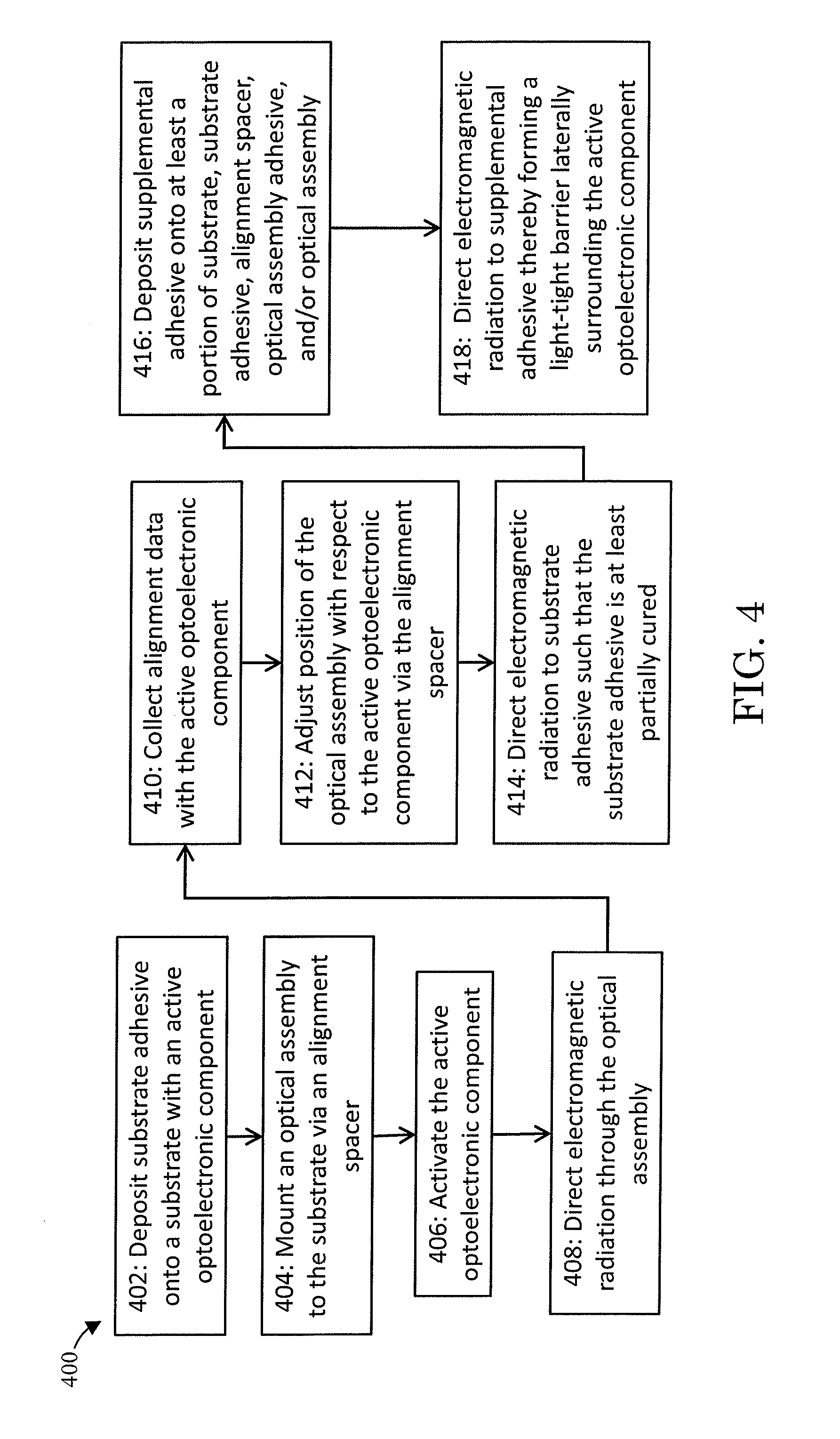
[0032] FIG. 4 depicts an example method for manufacturing an optoelectronic module having one or more alignment spacers.
DETAILED DESCRIPTION
[0033] As shown in FIG. 1A, an optoelectronic module 100 includes an optical assembly 103, an alignment spacer 105, a substrate 107, and an active optoelectronic component 109 mounted to the substrate 107. The optoelectronic module 100 can be any module operable to collect light, emit light, or both. For example, the optoelectronic module 100 can be a proximity sensor, two-dimensional camera, three-dimensional camera, time-of-flight camera, pattern or encoded-light projector, or an image projector.
[0034] The optical assembly 103, as mentioned above, can include optical elements 110 such as refractive or diffractive optical elements, a microlens array or any combination of the aforementioned. The optical elements 110 can be composed of optical resins or glasses and collectively may be characterized by a focal length F or other optical parameter necessary useful for the active alignment process. The optical assembly 103 can further include one or more apertures (e.g., composed of black chrome), and spectral filters (e.g., composed of polyester, resin, or dielectric materials). And can further include spacers or barrels configured to house the optical elements 110. The spacers or barrels can be manufactured by injection molding or may even be formed from non-transparent substrates (e.g., printed circuit boards) into which througholes (e.g., respectively filled with optically refractive material) have been incorporated.
[0035] The alignment spacer 105 is non-transparent and can be manufactured by injection molding in some instances. The alignment spacer 105 includes a first extension 111. In some instances, the optical assembly 103 can be fixed to the first extension 111 by an optical assembly adhesive 113. The optical assembly adhesive 113 can be at least partially cured by electromagnetic radiation (e.g., ultraviolet or infrared light). In other instances, the alignment spacer 105 may be integral to (e.g., manufactured with) the optical assembly 103 in which the first extension 111, and by inference the alignment spacer 105, would be subsumed into the optical assembly 103. For example, the optical assembly 103 can include a barrel that is configured to both house optical elements 110 and include a contiguous extension that forms the alignment spacer 105. In such instances, the alignment spacer 105 may be considered a portion of the optical assembly 103.
[0036] The alignment spacer 105 further includes a second extension 115. The first extension 111 and second extension 115 can be positioned on laterally opposing sides of the alignment spacer 105. The substrate 107 can be fixed to the second extension 115 by a substrate adhesive 117. The substrate 107 can be a printed circuit board, for example, or other material onto which the active optoelectronic component 109 can be suitably mounted, such as a lead frame. The active optoelectronic component 109 can be a light-emitting active optoelectronic component (e.g., a laser diode, a light emitting diode, or an array of each) or a light-sensitive active optoelectronic component (e.g., a photodiode, complimentary metal-oxide semiconductor- (CMOS) or charged-coupled device- (CCD) based image sensor). Accordingly, the active optoelectronic component can be operable to emit or be sensitive to a particular wavelength or range of wavelengths of electromagnetic radiation 118 (i.e., light).
[0037] As described above, since the optical assembly 103 is fixed to the alignment spacer 105, the alignment spacer 105 can be used to actively align the optical assembly 103 to the active optoelectronic component 109 and can be fixed in place by the substrate adhesive 117. The second extension 115 includes a surface 119 operable to limit the lateral migration of the substrate adhesive 117. By limiting the lateral migration of the substrate adhesive 117, the surface 119 can prevent the excess substrate adhesive 117 from migrating onto the active optoelectronic component 109, thereby permitting a smaller optoelectronic module footprint. Moreover, the substrate adhesive 117 can exhibit better mechanical stability, and provide a light-tight, gap-free bond line between the substrate 107 and the alignment spacer 105 as discussed in greater detail below.
[0038] FIG. 1A-FIG. 1C depict the example optoelectronic module 100 with different substrates 107 and different active optoelectronic components 109. FIG 1A depicts a light-sensitive active optoelectronic component 109 (depicted here as a CMOS or CCD image sensor) mounted to a substrate 107 (depicted here as a printed circuit board). The optical assembly 103 is characterized by a focal length F, and is aligned to the active optoelectronic component 109 via the spacer 107 and substrate adhesive 117 such that the distance between the optical assembly 103 and the active optoelectronic component 109 is substantially equal to the focal length F. In such instances, light 118 may be focused by the optical assembly 103 onto the active optoelectronic component 109.
[0039] FIG. 1B depicts a light-emitting active optoelectronic component 109 (depicted here as a light-emitting diode, laser diode, or an array of diodes) mounted to a substrate 107 (depicted here as a printed circuit board). Here to, the optical assembly 103 is characterized by a focal length F, and is aligned to the active optoelectronic component 109 via the spacer 107 and substrate adhesive 117 such that the distance between the optical assembly 103 and the active optoelectronic component 109 is substantially equal to the focal length F. In such instances, light 118 emitted by the active optoelectronic component 109 may be focused, projected, or amplified, for example, by the optical assembly 103. FIG. 1B also depicts supplemental adhesive 120. Supplemental adhesive 120 can be non-transparent to light 118. Further, supplemental adhesive 120 may be in contact with at least a portion of the optoelectronic module 100 (i.e., the supplemental adhesive 120 may be at least in partial contact with the substrate 107, substrate adhesive 117, alignment spacer 105, optical assembly adhesive 113, and/or optical assembly 103) thereby forming a light-tight barrier laterally surrounding the active optoelectronic component 109.
[0040] FIG. 1C depicts a light-emitting active optoelectronic component 109 (depicted here as a light-emitting diode, laser diode, or an array of diodes) mounted to a substrate 107 (depicted here as a lead frame). Again, the optical assembly 103 is characterized by a focal length F, and is aligned to the active optoelectronic component 109 via the spacer 107 and substrate adhesive 117 such that the distance between the optical assembly 103 and the active optoelectronic component 109 is substantially equal to the focal length F. In such instances, light 118 emitted by the active optoelectronic component 109 may be focused, projected, or amplified, for example, by the optical assembly 103.
[0041] FIG. 2A-FIG. 2C depict an enlarged view of a portion of the optoelectronic module 100 depicted in FIG. 1A-FIG. 1C. FIG. 2A depicts the second extension 115 of the alignment spacer 105. As described above, the extension includes a surface 119 operable to limit the lateral migration of substrate adhesive 117. The second extension 115 is chamfered at an angle .quadrature. as in the depicted example such that the surface 119 is operable to draw substrate adhesive 117 away from the substrate 107. Surface interaction between the the substrate adhesive 117 and the surface 119, together with other factors, such as adhesive viscosity, specific gravity, thixotropic index, and chamfer angle .quadrature., can be refined such that the substrate adhesive 117 is drawn away from the substrate 107 as depicted. For example, the substrate adhesive 117 can have an as deposited viscosity of 54,000 mPa.quadrature.s, a specific gravity of 1.3 g/cm.sup.3, a thixotropic index of 4.4 ( 1/10 s.sup.-1), and a chamfer angle .quadrature. of 30.degree..
[0042] FIG. 2A-FIG. 2C depict the same second extension 115 of the alignment spacer 105 but each figure depicts a different gap G between the alignment spacer 105 and the substrate 107, and a lateral spread L of the the substrate adhesive 107 (i.e., the bond line width). FIG. 2A-FIG. 2C illustrate a number of acceptable gaps G and lateral spreads L that may be accommodated by the alignment spacer 105. In each case, some excess substrate adhesive 117 is drawn away from the substrate 107. In some instances, for example as depicted in FIG. 2B and FIG. 2C, substrate adhesive 117 can adheres to a greater area (i.e., a greater portion of the surface 119) thereby enhancing mechanical stability.
[0043] FIG. 3A-FIG. 3D depict an enlarged view of a portion of the optoelectronic module 100 depicted in FIG. 1A-FIG. 1C with a number of different example alignment spacers. FIG. 3A depicts a substrate 107 with a socket 127. The socket 127 can be configured such that the second extensions 115 can be integrated within the socket 127. In this instance, substrate adhesive 117 can be limited by the socket 127 as well as the surface 119. FIG. 3B depicts another version of the socket 127. In this instance, the socket 127 may be chamfered such that the second extension 115 may be integrated within the socket 127. As above, both the socket 127 and the surface 119 may limit the lateral migration of the substrate adhesive 117.
[0044] FIG. 3C depicts an alignment spacer 105 with a chamfered second extension 115. The chamfered second extension 115 delineating the surface 119 includes at least one groove 121. In this instance, substrate adhesive 117 may be drawn away from the substrate 107 and the groove may be act as a reservoir for excess substrate adhesive 117 thereby limiting the lateral migration of substrate adhesive 117.
[0045] FIG. 3D depicts an alignment spacer 105 wherein the second extension 115 includes a groove 123. FIG. 3D also depicts a substrate 107 with an alignment extensions 125. The alignment extension 125 is operable to be integrated within the groove 123. In this, and other configurations, eye-safety may be maintained even if, for example, delamination of the substrate adhesive 117 occurs.
[0046] FIG. 4 depicts an example method for manufacturing an optoelectronic module having one or more alignment spacers. In a step 402, substrate adhesive 117 is deposited onto a substrate 107 with an active optoelectronic component 109.
[0047] In another step 404, an optical assembly 103 is mounted to the substrate 107 via an alignment spacer 105. In another step 406, the active optoelectronic component 109 is activated. For example, in instances where the active optoelectronic component 109 is light-sensitive, the component 109 is powered-up, initialized and in other ways made ready to collect light and store intensity values. In other instances, for example, where the active optoelectronic component 109 is light-emitting, the component 109 is powered-up and made to generate light.
[0048] In another step 408, electromagnetic radiation is directed through the optical assembly 103. For example, electromagnetic radiation can be focused by one or more optical elements within the optical assembly 103 either on the optoelectronic component 109 (in instance where the component 109 is light sensitive) or onto an imaging device external to the optoelectronic module 100 (in instances where the component 109 is light emitting).
[0049] In another step 410, alignment data is collected with the active optoelectronic component 109. That is, the active optoelectronic component 109 can be used to collect data in instances where the component 109 is light sensitive, or an imaging device external to the optoelectronic module 100 can be used to collect data in instances where the component 109 is light-emitting.
[0050] In another step 412, the position of the optical assembly 103 with respect to the active optoelectronic component 109 is adjusted via the alignment spacer 105. In instances where the optical assembly 103 includes optical elements 110 characterized by a focal length, the position of the optical assembly 103 can be adjusted until the focal length is incident on the active optoelectronic component 109.
[0051] In another step 414, electromagnetic radiation is directed to the substrate adhesive 117 such that the substrate adhesive 117 is at least partially cured. The electromagnetic radiation can be infrared or ultraviolet, for example.
[0052] In another step 416, supplemental adhesive 120 is deposited onto at least a portion of the substrate 107, substrate adhesive 117, alignment spacer 105, optical assembly adhesive 113, and/or optical assembly 115.
[0053] In another step 418, electromagnetic radiation is directed onto supplemental adhesive 120 thereby forming a light-tight barrier laterally surrounding the active optoelectronic component. The electromagnetic radiation can be infrared or ultraviolet, for example.
[0054] Various modifications may be made to the foregoing implementations. Features described above in different implementations may be combined in the same implementations. Thus, other implementations are within the scope of the claims.
* * * * *
D00000
D00001
D00002
D00003
D00004
XML
uspto.report is an independent third-party trademark research tool that is not affiliated, endorsed, or sponsored by the United States Patent and Trademark Office (USPTO) or any other governmental organization. The information provided by uspto.report is based on publicly available data at the time of writing and is intended for informational purposes only.
While we strive to provide accurate and up-to-date information, we do not guarantee the accuracy, completeness, reliability, or suitability of the information displayed on this site. The use of this site is at your own risk. Any reliance you place on such information is therefore strictly at your own risk.
All official trademark data, including owner information, should be verified by visiting the official USPTO website at www.uspto.gov. This site is not intended to replace professional legal advice and should not be used as a substitute for consulting with a legal professional who is knowledgeable about trademark law.