Semiconductor Device And Method For Manufacturing Same
Shinohara; Koji
U.S. patent application number 15/919761 was filed with the patent office on 2019-03-07 for semiconductor device and method for manufacturing same. The applicant listed for this patent is Kabushiki Kaisha Toshiba, Toshiba Electronic Devices & Storage Corporation. Invention is credited to Koji Shinohara.
| Application Number | 20190074839 15/919761 |
| Document ID | / |
| Family ID | 65518313 |
| Filed Date | 2019-03-07 |


| United States Patent Application | 20190074839 |
| Kind Code | A1 |
| Shinohara; Koji | March 7, 2019 |
SEMICONDUCTOR DEVICE AND METHOD FOR MANUFACTURING SAME
Abstract
A method for manufacturing a semiconductor device includes forming a circuit including a plurality of flip-flops, a plurality of first switches, a second switch and a signal line on a wafer, the flip-flops being connected in series through the first switches, respectively, and the signal line being connected to the second switch, and being configured to supply a signal in parallel to the flip-flops; testing the flip-flops by turning off the first switches, turning on the second switch, and supplying a test signal in parallel through the signal line to the flip-flops; and cutting at least one interconnect of a switch portion in the circuit, the switch portion including the first switches and the second switch, so that the first switch is turned on and the second switch is turned off.
| Inventors: | Shinohara; Koji; (Oita Oita, JP) | ||||||||||
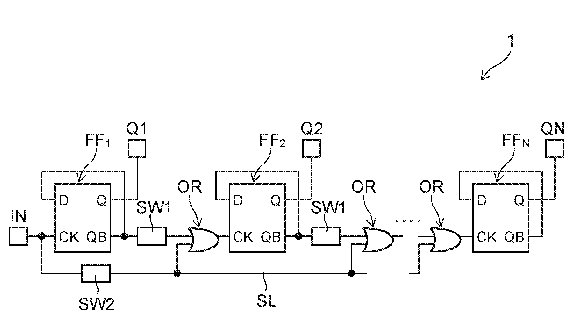
| Applicant: |
|
||||||||||
|---|---|---|---|---|---|---|---|---|---|---|---|
| Family ID: | 65518313 | ||||||||||
| Appl. No.: | 15/919761 | ||||||||||
| Filed: | March 13, 2018 |
| Current U.S. Class: | 1/1 |
| Current CPC Class: | H01L 21/76894 20130101; H01L 27/092 20130101; H01L 23/528 20130101; H03K 21/40 20130101; H01L 21/76892 20130101; H01L 22/14 20130101; H01L 21/78 20130101; H03K 21/10 20130101; H01L 22/32 20130101; H01L 22/20 20130101; H01L 21/823871 20130101 |
| International Class: | H03K 21/10 20060101 H03K021/10; H01L 21/8238 20060101 H01L021/8238; H01L 21/66 20060101 H01L021/66; H01L 21/768 20060101 H01L021/768; H01L 21/78 20060101 H01L021/78; H01L 27/092 20060101 H01L027/092; H01L 23/528 20060101 H01L023/528; H03K 21/40 20060101 H03K021/40 |
Foreign Application Data
| Date | Code | Application Number |
|---|---|---|
| Sep 5, 2017 | JP | 2017-170045 |
Claims
1. A method for manufacturing a semiconductor device, the method comprising: forming a circuit including a plurality of flip-flops, a plurality of first switches, a second switch and a signal line on a wafer, the flip-flops being connected in series through the first switches, respectively, and the signal line being connected to the second switch, and being configured to supply a signal in parallel to the flip-flops; testing the flip-flops by turning off the first switches, turning on the second switch, and supplying a test signal in parallel through the signal line to the flip-flops; and cutting at least one interconnect of a switch portion in the circuit, the switch portion including the first switches and the second switch, so that the first switches are turned on, and the second switch is turned off.
2. The method according to claim 1, wherein a plurality of integrated circuits are formed on the wafer, the integrated circuits including the flip-flops, the first switches, the second switch, and the signal line, a part of the at least one interconnect being provided in a space between one of the integrated circuits and the other integrated circuit adjacent thereto, and the at least one interconnect being cut at the part provided in the space.
3. The method according to claim 2, wherein the at least one interconnect is cut in a process of dicing the wafer into a plurality of chips including the integrated circuits respectively.
4. The method according to claim 2, wherein the at least one interconnect is cut in a process of etching a portion of the wafer exposed in the space.
5. The method according to claim 1, wherein a part of the at least one interconnect is melted in a process of cutting the at least one interconnect.
6. The method according to claim 5, wherein the part of the at least one interconnect is melted by laser irradiation.
7. The method according to claim 1, wherein the test signal inputted in parallel to the flip-flops makes outputs thereof to be inverted.
8. A semiconductor device comprising: a substrate; and an integrated circuit provided on a front surface of the substrate, the integrated circuit including a plurality of flip-flops connected in series, a plurality of first switches, a second switch, and a signal line, the flip-flops being connected in series through the first switches, respectively, and the signal line being connected to the second switch and provided to supply a signal in parallel to the plurality of flip-flops, wherein the integrated circuit includes a switch portion including the first switches and the second switch, at least one interconnect of the switch portion is cut so that the first switch is turned on and the second switch is turned off, and the integrated circuit includes a pair of cut ends divided at one position in the at least one interconnect.
9. The device according to claim 8, wherein the integrated circuit includes the pair of cut ends positioned at an outer edge thereof.
10. The device according to claim 8, further comprising: a logical sum gate provided between adjacent ones of the flip-flops, an output of the first switch and the signal being inputted to the logical sum gate, and an output of the logical sum gate being inputted to one of the adjacent ones of the flip-flops.
11. The device according to claim 10, wherein the first switches are each placed between one of the flip-flops and the logical sum gate.
12. The device according to claim 10, wherein the signal line includes a first portion connected to one of the flip-flops at an initial stage and an input of the second switch, and a second portion connected to an output of the second switch and other ones of the flip-flops at second and subsequent stages.
13. The device according to claim 10, wherein the first switches and the second switch are configured so that output potential is Low when being turned off.
14. The device according to claim 8, wherein the integrated circuit includes a first pair of cut ends for turning one of the first switches on, and a second pair of cut ends for turning the second switch off.
15. The device according to claim 14, wherein the first switches are each configured so that gate input is High when being turned on, and the second switch is configured so that gate input is Low when being turned off.
16. The device according to claim 8, wherein the integrated circuit includes one pair of cut ends for turning the first switches on, and turning the second switch off.
17. The device according to claim 16, wherein one of the pair of cut ends is connected to a common gate input of the first switch and the second switch.
18. The device according to claim 8, wherein the first switches and the second switch each include an NMOS transistor and a PMOS transistor connected in parallel.
Description
CROSS-REFERENCE TO RELATED APPLICATIONS
[0001] This application is based upon and claims the benefit of priority from Japanese Patent Application No. 2017-170045, filed on Sep. 5, 2017; the entire contents of which are incorporated herein by reference.
FIELD
[0002] Embodiments generally relate to a semiconductor device and a method for manufacturing the same.
BACKGROUND
[0003] A circuit such as a counter circuit has a configuration in which a plurality of flip-flops are connected in series. Each flip-flop is sequentially operated from the initial stage in the operation test of this circuit. Thus, it takes a long test time to verify the operation of all the flip-flops.
BRIEF DESCRIPTION OF THE DRAWINGS
[0004] FIG. 1 is a block diagram showing a circuit configuration of a semiconductor device according to an embodiment;
[0005] FIGS. 2A and 2B are circuit diagrams showing a switch circuit according to the embodiment;
[0006] FIGS. 3A and 3B are circuit diagrams showing another switch circuit according to the embodiment;
[0007] FIGS. 4A and 4B are schematic diagrams showing a circuit operation according to the embodiment;
[0008] FIG. 5 is a flow chart showing a manufacturing method of the semiconductor device according to the embodiment;
[0009] FIGS. 6A to 6C are schematic views showing the manufacturing method of the semiconductor device according to the embodiment; and
[0010] FIGS. 7A and 7B are circuit diagrams showing a switch circuit according to a variation of the embodiment.
DETAILED DESCRIPTION
[0011] According to one embodiment, a method for manufacturing a semiconductor device includes forming a circuit including a plurality of flip-flops, a plurality of first switches, a second switch and a signal line on a wafer, the flip-flops being connected in series through the first switches, respectively, and the signal line being connected to the second switch, and being configured to supply a signal in parallel to the flip-flops; testing the flip-flops by turning off the first switches, turning on the second switch, and supplying a test signal in parallel through the signal line to the flip-flops; and cutting at least one interconnect of a switch portion in the circuit, the switch portion including the first switches and the second switch, so that the first switches are turned on and the second switch is turned off.
[0012] Embodiments will now be described with reference to the drawings. The same portions inside the drawings are marked with the same numerals; a detailed description is omitted as appropriate; and the different portions are described. The drawings are schematic or conceptual; and the relationships between the thicknesses and widths of portions, the proportions of sizes between portions, etc., are not necessarily the same as the actual values thereof. The dimensions and/or the proportions may be illustrated differently between the drawings, even in the case where the same portion is illustrated.
[0013] There are cases where the dispositions of the components are described using the directions of XYZ axes shown in the drawings. The X-axis, the Y-axis, and the Z-axis are orthogonal to each other. Hereinbelow, the directions of the X-axis, the Y-axis, and the Z-axis are described as an X-direction, a Y-direction, and a Z-direction. Also, there are cases where the Z-direction is described as upward and the direction opposite to the Z-direction is described as downward.
[0014] FIG. 1 is a block diagram showing a circuit configuration of a semiconductor device according to an embodiment. A circuit shown in FIG. 1 is e.g. an asynchronous counter circuit 1. The circuit has a configuration in which flip-flops FF.sub.1-FF.sub.N (N: an integer of two or more) are connected in series. Each flip-flop FF has a data input D, a clock input CK, an output Q, and an inverted output QB. The flip-flop FF has a configuration in which the inverted output QB is fed back to the data input D. In the following description, there is a case where the flip-flops FF.sub.1-FF.sub.N are described individually, or collectively referred to as "flip-flop FF".
[0015] As shown in FIG. 1, a switch SW1 and a logical sum gate OR are each placed between the flip-flop FF.sub.P-1 and the flip-flop FF.sub.P (P: an integer of two or more and N or less). The input of the switch SW1 is connected to the inverted output QB of the flip-flop FF. The output of the switch SW1 is connected to the input of the logical sum gate OR. The output of the logical sum gate OR is connected to the clock input CK of the flip-flop FF.
[0016] The counter circuit 1 further includes a signal line SL connected in parallel to the input of each logical sum gate OR. A signal supplied to the clock input CK of the first stage flip-flop FF.sub.1 is also supplied in parallel by the signal line SL to each clock input CK of the flip-flops FF.sub.2-FF.sub.N through a switch SW2.
[0017] FIGS. 2A and 2B are circuit diagrams showing the switch circuit SW1. FIG. 2A is a circuit diagram showing the switch SW1 provided on a wafer. FIG. 2B is a circuit diagram showing the switch SW1 included in a semiconductor device after being divided into chips.
[0018] As shown in FIG. 2A, the switch SW1 includes transistors Tr1-Tr3, inverters NT1 and NT2. The transistors Tr1 and Tr3 are e.g. N-channel MOS (hereinafter NMOS) transistors. The transistor Tr2 is e.g. a P-channel MOS (hereinafter PMOS) transistor.
[0019] The input (IN) of the switch SW1 is connected to the drains of the transistors Tr1 and Tr2, for example. The output (OUT) of the switch SW1 is connected to the sources of the transistors Tr1 and Tr2, for example. The output of the switch SW1 is grounded through the transistor Tr3. That is, the transistor Tr3 has the drain connected to the output of the switch SW1, and the source of ground potential.
[0020] A gate potential is supplied to the gate of the transistor Tr1 through the inverters NT1 and NT2. The gate potential is also supplied to each gate of the transistors Tr2 and Tr3 through the inverter NT1.
[0021] As shown in FIG. 2A, the power supply line Vdd is grounded through a resistor R. A potential on the GND side of the resistor R is inputted to the inverter NT1. Thus, the potential Low is inputted to the inverter NT1. Accordingly, the output potential of the inverter NT1 is High, and supplied to each gate of the transistors Tr2 and Tr3. Thus, the transistor Tr2 is turned to the OFF state, and the transistor Tr3 is turned to the ON state. On the other hand, the output potential High of the inverter NT1 is inputted to the inverter NT2. Thus, the output potential of the inverter NT2 is Low, and inputted to the gate of the transistor Tr1. Thus, the transistor Tr1 is turned to the OFF state.
[0022] Thus, in the wafer state, the input/output path of the switch SW1 is turned OFF. The output of the switch SW1 is placed at the GND potential, i.e. Low.
[0023] In the example shown in FIG. 2B, the interconnect WR1 between the resistor R and GND is cut such that a part of the interconnect WR1 on the resistor R side is connected to the input of the inverter NT1. The interconnect WR1 connected to the input of the inverter NT1 includes a cut end TM1 on the resistor R side.
[0024] As described later, the interconnect WR1 is cut in the process for forming the semiconductor device chip. Thus, in the semiconductor device after being diced, the potential High of the power supply line Vdd is inputted to the inverter NT1 through the resistor R. Accordingly, the output potential of the inverter NT1 is Low, and supplied to each gate of the transistors Tr2 and Tr3. Then, the transistor Tr2 is turned to the ON state, and the transistor Tr3 is turned to the OFF state. Moreover, the output potential of the inverter NT2 is High, and supplied to the gate of the transistor Tr1. Then, the transistor Tr1 is turned to the ON state. As a result, in the semiconductor device after being diced, the input/output path of the switch SW1 is in the ON state.
[0025] FIGS. 3A and 3B are circuit diagrams showing the switch SW2. FIG. 3A is a circuit diagram showing the switch SW2 provided on a wafer. FIG. 3B is a circuit diagram showing the switch SW2 included in a semiconductor device after being diced.
[0026] As shown in FIGS. 3A and 3B, the switch SW2 includes transistors Tr1-Tr3, inverters NT1 and NT2. The switch SW2 is different from the switch SW1 shown in FIG. 2A in that the input of the inverter NT1 is connected to Vdd side of the resistor R.
[0027] As shown in FIG. 3A, the potential High of the power supply line Vdd is inputted to the inverter NT1 of the switch SW2. Thus, the output potential of the inverter NT1 is Low, and supplied to each gate of the transistors Tr2 and Tr3. Then, the transistor Tr2 is turned to the ON state, and the transistor Tr3 is turned to the OFF state. Moreover, the output potential of the inverter NT2 is High, and supplied to the gate of the transistor Tr1. Then, the transistor Tr1 is turned to the ON state. As a result, in the wafer state, the switch SW2 is in the ON state.
[0028] As shown in FIG. 3B, the interconnect WR2 is cut between the power supply line Vdd and the resistor R. A part of the interconnect WR2 on the resistor R side is connected to the input of the inverter NT1. The part of the interconnect WR2 connected to the input of the inverter NT1 includes an end TM2 on the resistor side.
[0029] The interconnect WR2 is also cut in the process of forming the semiconductor device chip. In the semiconductor device after being diced, the potential Low of GND is inputted to the inverter NT1 of the switch SW2 through the resistor R. Accordingly, the output potential of the inverter NT1 is High, and supplied to each gate of the transistors Tr2 and Tr3. Then, the transistor Tr2 is turned to the OFF state, and the transistor Tr3 is turned to the ON state. The output of the switch SW2 is the GND potential, i.e. Low.
[0030] On the other hand, the output potential of the inverter NT2 is Low, and supplied to the gate of the transistor Tr1. Then, the transistor Tr1 is turned to the OFF state. As a result, in the semiconductor device after being diced, the input/output path of the switch SW2 is in the OFF state. The output of the switch SW2 is Low.
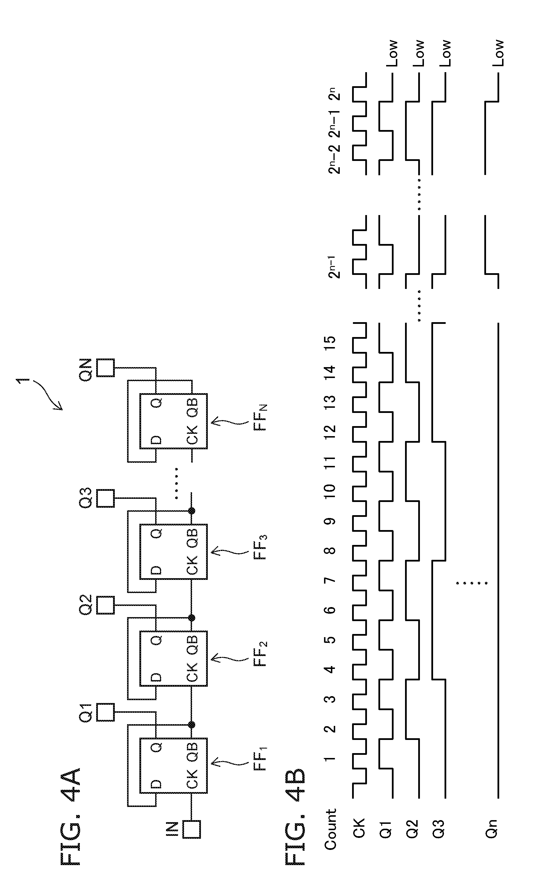
[0031] FIGS. 4A and 4B are schematic diagrams showing an operation of the counter circuit 1. FIG. 4A is a block diagram showing the configuration of the counter circuit 1 included in the semiconductor device after being diced. FIG. 4B is a time chart showing the operation of the counter circuit 1.
[0032] As described above, in the semiconductor device after being diced, the switch SW1 is in the ON state, and the switch SW2 is in the OFF state. The output of the switch SW2 is Low, and the input from the signal line SL to the logical sum gate OR is constantly Low. Thus, as shown in FIG. 4A, the counter circuit 1 may be considered to operate in the configuration in which the switches SW1, SW2, the logical sum gate OR, and the signal line SL are omitted.
[0033] FIG. 4B shows a clock signal supplied to the clock input CK of flip-flop FF.sub.1 at the first stage, and outputs Q1, Q2, Q3, QN of the flip-flops FF.sub.1, FF.sub.2, FF.sub.3, FF.sub.N. Each flip-flop FF detects e.g. the rising from Low to High of the clock signal supplied to the clock input CK, and inverts the output thereof.
[0034] As shown in FIG. 4B, at the rising timing of count 1 of the clock signal, the flip-flop FF.sub.1 at the first stage inverts the output Q1 thereof from Low to High. Then, the inverted output QB of the flip-flop FF.sub.1 is Low. Thus, the clock input CK of the second stage flip-flop FF.sub.2 is Low, and the output Q2 thereof is held Low.
[0035] Subsequently, at the rising timing of count 2 of the clock signal, the flip-flop FF.sub.1 inverts the output Q1 thereof from High to Low. At this time, the inverted output QB of the flip-flop FF.sub.1 is turned to High and inputted to the clock input CK of the flip-flop FF.sub.2 at the second stage. Then, the output Q2 of the flip-flop FF.sub.2 is inverted from Low to High. The inverted output QB of the flip-flop FF.sub.2 is Low. The output Q3 of the flip-flop FF.sub.3 at the third stage is held Low.
[0036] Subsequently, at the rising timing of count 3 of the clock signal, the flip-flop FF.sub.1 at the initial stage inverts the output Q1 thereof from Low to High. Then, the inverted output QB of the flip-flop FF.sub.1 is inverted from High to Low. However, the output Q2 of the flip-flop FF.sub.2 at the second stage is held High. Thus, the inverted output QB of the flip-flop FF.sub.2 is Low. The output Q3 of the third stage flip-flop FF.sub.3 is held Low.
[0037] Subsequently, at the rising timing of count 4 of the clock signal, the flip-flop FF.sub.1 at the initial stage inverts the output Q1 thereof from High to Low. Then, the inverted output QB of the flip-flop FF.sub.1 is inverted from Low to High. The output Q2 of the flip-flop FF.sub.2 at the second stage is inverted from High to Low. The inverted output QB of the flip-flop FF.sub.2 is inverted from Low to High. According to the inverted output QB of the flip-flop FF.sub.2, the output Q3 of the flip-flop FF.sub.3 at the third stage is inverted from Low to High.
[0038] Thus, the outputs Q of the flip-flops FF.sub.1-FF.sub.N are sequentially inverted from Low to High. The timing of inverting the output Q of the n-th stage flip-flop FF is 2.sup.n-1.times.Tc seconds later. Here, Tc (seconds) is the clock cycle. For instance, the output Q of the last stage flip-flop FF.sub.N is inverted at the timing of 2.sup.N-1.times.Tc seconds later after the first clock count 1 is inputted. Furthermore, it requires 2.sup.N-1 clock counts until the outputs of all the flip-flops FF are inverted from Low to High, and all the output states are verified, which complete at (2.sup.N-1).times.Tc seconds later.
[0039] For instance, when the counter circuit having the configuration shown in FIG. 4A is formed on a wafer in place of the counter circuit 1 shown in FIG. 1, the time required to complete the operation test becomes longer as the number of stages increases in the flip-flops FF connected in series. Thus, it takes a longer time in an operation test of the semiconductor device in the wafer state to check the counter circuit. As a result, the throughput time of the manufacturing process may increase significantly.
[0040] In contrast, in the counter circuit 1 according to this embodiment, the switch SW1 is placed to operate each flip-flop FF independently. Thus, the clock signal can be inputted in parallel to the clock input CK of each flip-flop through the signal line SL. Accordingly, the operation test can be completed in a short time irrespective of the number of stages of flip-flops FF.
[0041] Furthermore, the interconnects WR1 and WR2 of the switches SW1 and SW2 are cut in the semiconductor device after being diced. Thus, the switch SW1 is turned to the ON state, and the switch SW2 is turned to the OFF state. Thereby, it is possible to achieve the operation similar to that of the simplified circuit shown in FIG. 4A.
[0042] Next, a manufacturing method of the semiconductor device according to the embodiment is described with reference to FIGS. 5 to 6C. FIG. 5 is a flow chart showing a method for manufacturing the semiconductor device according to the embodiment. FIGS. 6A to 6C are schematic views showing the method for manufacturing the semiconductor device according to the embodiment.
[0043] Step S01: An integrated circuit IC including a plurality of flip-flops FF is formed on a wafer 10. As shown in FIG. 6A, the integrated circuits IC are arranged with a constant pitch in the X-direction and the Y-direction on the front surface of the wafer 10. Each integrated circuit IC includes a plurality of flip-flops FF, switches SW1, SW2, a signal line SL, and a logical sum gate OR (see FIG. 1).
[0044] The plurality of flip-flops FF are connected in series via the switch SW1 and the logical sum gate OR. The inverted output QB of each flip-flop FF is inputted to the switch SW1 placed between each flip-flop FF and the flip-flop FF at the next stage. The output of the switch SW1 is connected to the input of the logical sum gate OR. The output of the logical sum gate OR is connected to the clock input CK of the flip-flop FF at the next stage. A clock signal is inputted by the signal line SL through the switch SW2. The signal line SL is connected to the input of each logical sum gate OR. The signal line SL supplies the clock signal in parallel through the logical sum gate OR to the clock input CK of each flip-flop FF.
[0045] The integrated circuit IC1 includes interconnects WR1 and WR2 of the switches SW1 and SW2 (see FIGS. 2 and 3). As shown in FIG. 6B, parts of the interconnects WR1 and WR2 is provided in a space 13 between the integrated circuit IC1 and an integrated circuit IC2 adjacent thereto.
[0046] Step S02: The operation test of each integrated circuit IC is performed in the wafer state. At this time, the switch SW1 is in the OFF state, and the switch SW2 is in the ON state. A clock signal is inputted to the terminal connected to the clock input CK of the initial stage flip-flop FF1 to check inversion of the output Q of each flip-flop FF. The clock signal is also supplied in parallel to the flip-flops FF of the second and subsequent stages through the switch SW2, the signal line SL, and the logical sum gate OR.
[0047] Step S03: The wafer 10 is divided into chips each including the integrated circuit IC. For instance, a dicing saw is used to cut the wafer 10 along the space 13 between the adjacent integrated circuits IC. Thereby, each semiconductor device is diced into chip. At this time, as shown in FIG. 6C, parts of the interconnects WR1 and WR2 are cut in the switches SW1 and SW2. The ends TM1 and TM2 of the interconnects of the switches SW1 and SW2 are exposed at the outer edge of each integrated circuit IC diced into chip.
[0048] The dicing process of the integrated circuit IC is not limited to the above method. For instance, the wafer 10 may be divided using a dicing saw or a scriber after the part of the space 13 exposed in the wafer 10 is selectively etched. In this case, the interconnects WR1 and WR2 are cut by the etching in the wafer 10.
[0049] In the embodiment, it is possible to reduce the time required to complete the operation test, in the wafer state, of the flip-flops FF connected in series. Furthermore, the switches SW1 and SW2 can be turned to the ON state and the OFF state, respectively, and thus, the flip-flops FF can operate as intended after being diced without an additional step for cutting the interconnects WR1 and WR2. The integrated circuit IC includes both cut ends of the interconnects WR1 and WR2, and the end surfaces thereof are placed at the outer edge of the integrated circuit IC.
[0050] FIGS. 7A and 7B are circuit diagrams showing a switch circuit SC according to a variation of the embodiment. FIG. 7A is the circuit diagram showing the switch circuit SC in a wafer state. FIG. 7B is the circuit diagram showing the switch circuit SC included in a semiconductor device after being diced.
[0051] As shown in FIG. 7A, the switch circuit SC includes a plurality of switches SW1 and a switch SW2. The switches SW1 are placed respectively between flip-flops connected in series. The switch SW2 is placed between a terminal connected to the clock input CK of the flip-flop FF.sub.1 at the initial stage and a signal line SL.
[0052] A gate bias is supplied from a power supply line Vdd through inverters NT1, NT2, and NT3 to the gates of transistors Tr1, Tr2, and Tr3 included in the switches SW1 and SW2 (see FIGS. 2 and 3).
[0053] As shown in FIG. 7A, potential Low is inputted from the power supply line Vdd side to the inverter NT1. The output potential High of the inverter NT1 is supplied to the gate of the transistors Tr2 and Tr3 of each switch SW1. Furthermore, according to the output of the inverter NT1, the inverter NT2 outputs potential Low. The output of the inverter NT2 is supplied to the transistor Tr1 of each switch SW1. Thus, each switch SW1 is turned to the OFF state, and the output potential thereof is Low.
[0054] Furthermore, the output of the inverter NT2 is inputted to the inverter NT3. The inverter NT3 outputs potential High. The output of the inverter NT3 is supplied to the gate of the transistor Tr1 of the switch SW2 and turns the transistor Tr1 to the ON state. On the other hand, the output potential Low of the inverter NT2 is supplied to each gate of the transistors Tr2 and Tr3 of the switch SW2. Thus, the transistor Tr2 is turned to the ON state, and the transistor Tr3 is turned to the OFF state. As a result, the test operation mode of the wafer state is achieved in the counter circuit shown in FIG. 1.
[0055] As shown in FIG. 7B, the semiconductor device after being diced includes an interconnect WR3 connected to the input of the inverter NT1. The interconnect WR3 is connected between a resistor R and GND. The interconnect WR3 is cut in the semiconductor device after being diced. A part of the interconnect WR3 after cutting includes an end TM3, and is connected to the input of the inverter NT1. A potential High of the power supply line Vdd is supplied to the inverter NT1 after the interconnect WR3 is cut. Thus, the output of the inverters NT1, NT2, and NT3 is inverted. The switches SW1 are all turned to the ON state, and the switch SW2 is turned to the OFF state. Thus, the counter circuit 1 is placed in the normal operation mode.
[0056] A part of the interconnect WR3 is provided in a space 13 between the integrated circuits IC as shown in e.g. FIG. 6B. Thus, without an additional step for cutting the interconnect WR3, the counter circuit 1 can be switched from the test operation mode to the normal operation mode. In this example, one counter circuit has one cutting location of the interconnect. Thus, the interconnect WR3 may be cut by e.g. a method in which the interconnect WR3 is melted by laser irradiation.
[0057] While certain embodiments have been described, these embodiments have been presented by way of example only, and are not intended to limit the scope of the inventions. Indeed, the novel embodiments described herein may be embodied in a variety of other forms; furthermore, various omissions, substitutions and changes in the form of the embodiments described herein may be made without departing from the spirit of the inventions. The accompanying claims and their equivalents are intended to cover such forms or modifications as would fall within the scope and spirit of the invention.
* * * * *
D00000
D00001
D00002
D00003
D00004
D00005
D00006
D00007
XML
uspto.report is an independent third-party trademark research tool that is not affiliated, endorsed, or sponsored by the United States Patent and Trademark Office (USPTO) or any other governmental organization. The information provided by uspto.report is based on publicly available data at the time of writing and is intended for informational purposes only.
While we strive to provide accurate and up-to-date information, we do not guarantee the accuracy, completeness, reliability, or suitability of the information displayed on this site. The use of this site is at your own risk. Any reliance you place on such information is therefore strictly at your own risk.
All official trademark data, including owner information, should be verified by visiting the official USPTO website at www.uspto.gov. This site is not intended to replace professional legal advice and should not be used as a substitute for consulting with a legal professional who is knowledgeable about trademark law.