Antenna structures having planar inverted F-antenna that surrounds an artificial magnetic conductor cell
CONTOPANAGOS; Harry
U.S. patent application number 16/121519 was filed with the patent office on 2019-03-07 for antenna structures having planar inverted f-antenna that surrounds an artificial magnetic conductor cell. The applicant listed for this patent is Energous Corporation. Invention is credited to Harry CONTOPANAGOS.
| Application Number | 20190074133 16/121519 |
| Document ID | / |
| Family ID | 63294941 |
| Filed Date | 2019-03-07 |


View All Diagrams
| United States Patent Application | 20190074133 |
| Kind Code | A1 |
| CONTOPANAGOS; Harry | March 7, 2019 |
Antenna structures having planar inverted F-antenna that surrounds an artificial magnetic conductor cell
Abstract
Integrated antenna structures described herein include, as one example, a multi-layered printed circuit board (PCB), including an artificial magnetic conductor (AMC) cell that includes a backing metal layer defining a first inner layer of the multi-layered PCB and an AMC metal layer defining a second inner layer of the multi-layered PCB. The metal layer defining the second inner layer is separated from at least one edge of the multi-layered PCB, and a planar inverted F antenna (PIFA) surrounds the AMC cell. The AMC metal layer is configured to reflect energy radiated by the PIFA. In some embodiments, the energy radiated by the PIFA includes radio frequency waves that can be used by a receiver to power or charge an electronic device.
| Inventors: | CONTOPANAGOS; Harry; (Kifissia, GR) | ||||||||||
| Applicant: |
|
||||||||||
|---|---|---|---|---|---|---|---|---|---|---|---|
| Family ID: | 63294941 | ||||||||||
| Appl. No.: | 16/121519 | ||||||||||
| Filed: | September 4, 2018 |
Related U.S. Patent Documents
| Application Number | Filing Date | Patent Number | ||
|---|---|---|---|---|
| 14586134 | Dec 30, 2014 | 10068703 | ||
| 16121519 | ||||
| 14336971 | Jul 21, 2014 | 9871301 | ||
| 14586134 | ||||
| Current U.S. Class: | 1/1 |
| Current CPC Class: | H01Q 15/0006 20130101; H01Q 1/38 20130101; H01F 27/2804 20130101; H01Q 1/273 20130101; H01Q 19/10 20130101; H01Q 19/185 20130101; H02J 50/20 20160201; H01F 38/14 20130101; H01Q 3/44 20130101; H01Q 9/0421 20130101; H02J 50/005 20200101; H01Q 1/243 20130101; H02J 50/23 20160201; H01Q 13/10 20130101; H01Q 15/0086 20130101 |
| International Class: | H01F 38/14 20060101 H01F038/14; H01Q 9/04 20060101 H01Q009/04; H01F 27/28 20060101 H01F027/28; H02J 50/20 20160101 H02J050/20; H01Q 15/00 20060101 H01Q015/00 |
Claims
1. (canceled)
2. An antenna structure comprising: a multi-layered printed circuit board (PCB), comprising an artificial magnetic conductor (AMC) cell that includes (i) a backing metal layer defining a first inner layer of the multi-layered PCB and (ii) an AMC metal layer defining a second inner layer of the multi-layered PCB, wherein the metal layer defining the second inner layer is separated from at least one edge of the multi-layered PCB; and a planar inverted F antenna (PIFA) surrounding the AMC cell, wherein the AMC metal layer is configured to reflect energy radiated by the PIFA.
3. The antenna structure of claim 2, wherein the AMC metal layer is separated from all edges of the multi-layered PCB.
4. The antenna structure of claim 2, wherein the AMC metal layer has a square shape.
5. The antenna structure of claim 4, wherein the square shape includes a metal divider that defines at least one inner rectangle.
6. The antenna structure of claim 5, wherein the metal divider defines at least two inner rectangles, each of the two inner rectangles have a same set of dimensions, and the same set of dimensions determining the frequency tuning and bandwidth of the AMC cell.
7. The antenna structure of claim 2, wherein the AMC metal layer is configured to reflect energy radiated by the PIFA to produce a directional radiation pattern.
8. The antenna structure of claim 2, wherein the AMC metal layer comprises a metamaterial.
9. The antenna structure of claim 2, wherein: the PIFA further comprises an antenna element disposed over a part of a top portion of the multi-layered PCB and a ground element disposed over a part of a bottom portion of the multi-layered PCB, and the antenna element is coupled to the ground element and a different part of the bottom portion of the multi-layered PCB through a first ground via and a signal via, respectively, and the antenna structure further includes a folded ground formed over a different part of the top portion of the multi-layered PCB, and the folded ground is coupled to the ground element through a second ground via.
10. The antenna structure of claim 8, wherein the ground element comprises a ground slot and the antenna element comprises an antenna slot.
11. The antenna structure of claim 8, wherein the top and bottom portions of the multi-layered printed circuit board PCB comprise a conductive metal.
12. The antenna structure of claim 2, wherein a transmitter coupled to the PIFA is configured to provide a signal for radiation by the PIFA.
13. The antenna structure of claim 10, wherein the transmitter comprises a processing apparatus for adjusting at least one of a phase of the signal and a magnitude of the signal.
14. The antenna structure of claim 2, wherein the energy radiated by the PIFA includes radio frequency waves.
15. The antenna structure of claim 14, wherein the radio frequency waves are used by a receiver to power or charge an electronic device.
16. An apparatus for providing 3-dimensional pockets of energy through pocket-forming, the apparatus comprising: a multi-layered printed circuit board (PCB), comprising a plurality of artificial magnetic conductor (AMC) cells, wherein each of the AMC cells comprises a backing metal layer and an AMC metal layer defining inner layers of the multi-layered PCB and is separated from at least one edge of the multi-layered PCB, wherein each of the AMC layers is configured to reflect energy independently as radiated by each of a plurality of planar inverted F antennas (PIFAs) to enable pocket-forming of energy; and wherein each of the PIFAs surrounding at least one AMC cell of the plurality of the AMC cells.
17. The apparatus of claim 16, wherein each of the AMC metal layers is separated from all edges of the multi-layered PCB.
18. The apparatus of claim 16, wherein each of the AMC metal layers has a square shape.
19. The apparatus of claim 18, wherein each of the square shapes includes a metal divider that defines at least one inner rectangle.
20. The apparatus of claim 19, wherein the metal divider defines at least two inner rectangles, each of the two inner rectangles have a same set of dimensions, and the same set of dimensions determining the frequency tuning and bandwidth of the AMC cells.
21. The apparatus of claim 16, wherein at least one of the AMC metal layers is configured to reflect energy radiated by at least one of the plurality of PIFAs to produce a directional radiation pattern.
Description
CROSS-REFERENCE TO RELATED APPLICATIONS
[0001] This application is a continuation of U.S. patent application Ser. No. 14/586,134, filed on Dec. 30, 2014, entitled "Integrated Miniature PIFA With Artificial Magnetic Conductor Metamaterials," which is a continuation-in-part of U.S. patent application Ser. No. 14/336,971, filed on Jul. 21, 2014, entitled "Integrated Miniature PIFA with Artificial Magnetic Conductor Metamaterials," (U.S. Pat. No. 9,871,301), each of which is herein fully incorporated by reference in its respective entirety
[0002] This application is related to U.S. Non-Provisional patent application Ser. No. 14/583,625, filed Dec. 27, 2014, entitled "Receivers for Wireless Power Transmission," U.S. Non-Provisional patent application Ser. No. 14/583,630, filed Dec. 27, 2014, entitled "Methodology for Pocket-Forming," U.S. Non-Provisional patent application Ser. No. 14/583,634, filed Dec. 27, 2014, entitled "Transmitters for Wireless Power Transmission," U.S. Non-Provisional patent application Ser. No. 14/583,640, filed Dec. 27, 2014, entitled "Methodology for Multiple Pocket-Forming," U.S. Non-Provisional patent application Ser. No. 14/583,641, filed Dec. 27, 2014, entitled "Wireless Power Transmission with Selective Range," U.S. Non-Provisional patent application Ser. No. 14/583,643, filed Dec. 27, 2014, entitled "Method for 3 Dimensional Pocket-Forming," all of which are incorporated herein by reference in their entirety.
BACKGROUND
Field of the Disclosure
[0003] The present disclosure relates in general to antennas, and more specifically, to compact and directional planar inverted-F antennas (PIFAs) integrated in artificial magnetic conductor metamaterials which may be used for wireless power transmission.
Background
[0004] Wireless power transmission may include a transmitter for forming and directing radio frequency (RF) waves towards a receiver which may convert RF waves into usable power for charging or powering an electronic device. The receiver may be integrated in the electronic device (e.g., a smartphone, a tablet) or may be in the form of cases that may be operatively coupled with the electronic device for suitable charging or powering. The transmitter may be an antenna array that may include N antennas which may be directional.
[0005] The antenna array may be controlled by computer hardware and software in order to broadcast a wireless signal towards the receiver. Amplitude and phase among other properties of the transmitted RF waves may be tuned by the computer hardware and software to form constructive and destructive interference patterns generating pockets of energy in a 3-dimensional shape from the constructive patterns, and null spaces from the destructive patterns to aim the pockets of energy to specific receivers.
[0006] The number of antennas in the antenna array may vary in relation with the desired power range and transmission capability of the transmitter. The more antennas the wider the range and higher the power transmission potential available at the transmitter. More antennas may additionally enable the transmitter to target more receivers at once. Directional antenna designs that can be integrated in transmitters may include Yagi, log-periodic, corner reflectors, and parabolic antennas, among others.
[0007] However, size may be one important factor that may impact the number of antennas that can be integrated in the antenna array for the transmitter. Designers often look for the optimal combination of size and performance in the antennas integrated in the transmitter, where the performance is usually hampered when size is reduced.
[0008] Planar inverter F antennas (PIFA) may be fabricated in small form factors that may allow for dense antenna arrays. However, PIFA antennas' radiation pattern is commonly omnidirectional, which might mean than a transmitter including an antenna array of PIFA antennas may waste transmitted power. Additionally the omnidirectional radiation patterns may hinder the transmitter ability to focus the transmitted RF waves to specific receivers.
[0009] For the foregoing reasons, there is a need for a directional antenna that may enable for the construction of tightly packaged antenna arrays that may render reasonable small sizes of antenna arrays while keeping a suitable performance.
SUMMARY
[0010] Various embodiments of a PIFA integrated with artificial magnetic conductors (AMC) metamaterials described herein may include a PIFA, an AMC metal layer, and a backing metal conductor formed on a multi-layer printed circuit board (PCB).
[0011] In one exemplary embodiment of the present disclosure, a folded ground planar array inverted-F (PIFA) is disclosed. The folded ground PIFA may include an antenna element with two or more slots formed over the top layer of a PCB, where these antenna slots may be designed for reducing the area of the antenna while keeping a suitable impedance bandwidth. These PIFA configurations may also include a ground element formed on the bottom layer of the PCB and operatively coupled with the antenna element through ground and signal vias. The ground element may include a slot designed for reducing the area of the ground while increasing the radiation efficiency of the PIFA system. The missing central ground area does not affect antenna operation except possibly in de-tuning the impedance bandwidth, which can be adjusted by the antenna element itself.
[0012] In one embodiment, a PIFA configuration may include a folded ground formed over the empty space of a PCB top layer, without interfering with the operation of an antenna element which may be also formed over the PCB top layer. This folded ground may be operatively connected with a ground element on the PCB bottom layer through folded ground vias. Folded ground may allow the reduction in the system area while maintaining an omnidirectional radiation pattern and a suitable performance in terms of impedance bandwidth and radiation efficiency.
[0013] In another embodiment of the present disclosure, an AMC unit cell may include an AMC metal layer and a backing metal layer. The AMC metal layer and the backing metal layer may be formed in the inner layers of a multi-layer PCB. In some embodiments, the edges of the AMC metal layer may be close to the edges of the AMC unit cell but not coincident.
[0014] In one embodiment, the AMC metal layer of an AMC unit cell may exhibit a square .theta. ring shape, while in other embodiments, the AMC metal layer may exhibit a square ring shape. Yet in other embodiments, the AMC metal layer may be of any shape and size. The shape and dimensions of the AMC unit cell may determine the frequency tuning of AMC unit cell functionality.
[0015] In one embodiment of the present disclosure, a first AMC metamaterial embodiment may be formed with 5.times.5 array of AMC unit cells, where each AMC unit cell may include an AMC metal layer that may exhibit a square 0 ring shape and a backing metal layer. The first AMC metamaterial may be formed over a large multi-layer and monolithic PCB that may fit a plurality of AMC unit cells. According to some aspects of this embodiment, the 5.times.5 array of AMC unit cells may exhibit the properties of an AMC metamaterial. The AMC metamaterial may be tuned to a resonant frequency which may be designed to be the low-band edge of a desired frequency band.
[0016] In another embodiment, a second AMC metamaterial embodiment may be formed with 6.times.6 array of AMC unit cells, where each AMC unit cell may include an AMC metal layer which may exhibit a square ring shape, and a backing metal layer. The second AMC metamaterial may be formed over a large multi-layer and monolithic PCB that may fit a plurality of AMC unit cells. According to some aspects of this embodiment, the 5.times.5 array of AMC unit cells may exhibit the properties of an AMC metamaterial. The AMC metamaterial may be tuned to a resonant frequency which may be designed to be the low-band edge of a desired frequency band.
[0017] One exemplary embodiment of the present disclosure may include the integration of a PIFA with a first AMC metamaterial to form a first integrated antenna structure. In the first integrated antenna structure, the AMC metal layer and backing conductor of the first metamaterial may be formed on the inner layers of a four layer PCB, while antenna elements and ground elements of the PIFA may be formed on top and bottom layers of a PCB, respectively. In some embodiments, a hole may be made in the metal backing conductor to allow signal and ground vias from PIFA to traverse the backing metal layer without contact, while the folded ground vias in PIFA may be short-circuited with the backing metal layer.
[0018] Another exemplary embodiment of the present disclosure may include the integration of a PIFA with a second AMC metamaterial to form a second integrated antenna structure. In the second integrated antenna structure, the AMC metal layer and backing conductor of the second metamaterial embodiment may be formed on the inner layers of a four layer PCB, while antenna elements and ground elements of the PIFA may be formed on top and bottom layers of a PCB, respectively. In some embodiments, a hole may be made in the metal backing conductor to allow signal and ground vias from PIFA to traverse the backing metal layer without contact, while the folded ground vias in PIFA may be short-circuited with the backing metal layer.
[0019] In yet other embodiments, where the PIFA has no folded ground, folded ground vias of PIFA may still be formed in the PCB and be short-circuited with the backing metal layer.
[0020] According to some aspects of the present disclosure the integrated antenna structures may exhibit a directional radiator pattern.
[0021] The AMC metamaterial in the integrated antenna structures may operate as an artificial magnetic reflector that may send upwards all energy radiated by the PIFA, thus achieving a directional radiation pattern. More specifically, the integrated antenna structures may exhibit a directional broadside pattern that may be about twice of that of the omnidirectional radiation pattern exhibited by PIFA alone. In addition, the relatively small system area of the integrated antenna structures may enable the fabrication of compact directional antenna arrays that may be suitable for small system area transmitters. The relatively small system area of the integrated antenna structures described herein may be considerable smaller than those of traditional directional antennas.
[0022] Numerous other aspects, features and benefits of the present disclosure may be made apparent from the following detailed description taken together with the drawing figures.
BRIEF DESCRIPTION OF THE DRAWINGS
[0023] The present disclosure can be better understood by referring to the following figures. The components in the figures are not necessarily to scale, emphasis instead being placed upon illustrating the principles of the disclosure. In the figures, reference numerals designate corresponding parts throughout the different views.
[0024] FIG. 1A shows an isometric view of a planar inverted-F antenna integrated in a printed circuit board, according to an embodiment.
[0025] FIG. 1B illustrates a side view of planar inverted-F antenna integrated in a printed circuit board, according to an embodiment.
[0026] FIG. 2A shows an omnidirectional isometric radiation pattern of the PIFA, according to an embodiment.
[0027] FIG. 2B depicts the return loss of the PIFA when fed by a 50-Ohm port, according to an embodiment.
[0028] FIG. 3 illustrates a side view of an exemplary AMC unit cell of an AMC metamaterial, according to an embodiment.
[0029] FIG. 4A illustrates an isometric view of a unit cell of an AMC metamaterial that may include AMC metal layers resembling a square .theta. ring, according to an embodiment.
[0030] FIG. 4B illustrates a top view of the AMC unit cell of an AMC metamaterial, according to an embodiment.
[0031] FIG. 5 illustrates an isometric view a 5.times.5 array AMC unit cells of an AMC metamaterial that may include AMC metal layers that may resemble a .theta. square ring, according to an embodiment.
[0032] FIG. 6 illustrates the complex reflection coefficient of an incident plane wave at the surface of an AMC metamaterial that may include AMC metal layers that may resemble a square .theta. ring, according to an embodiment.
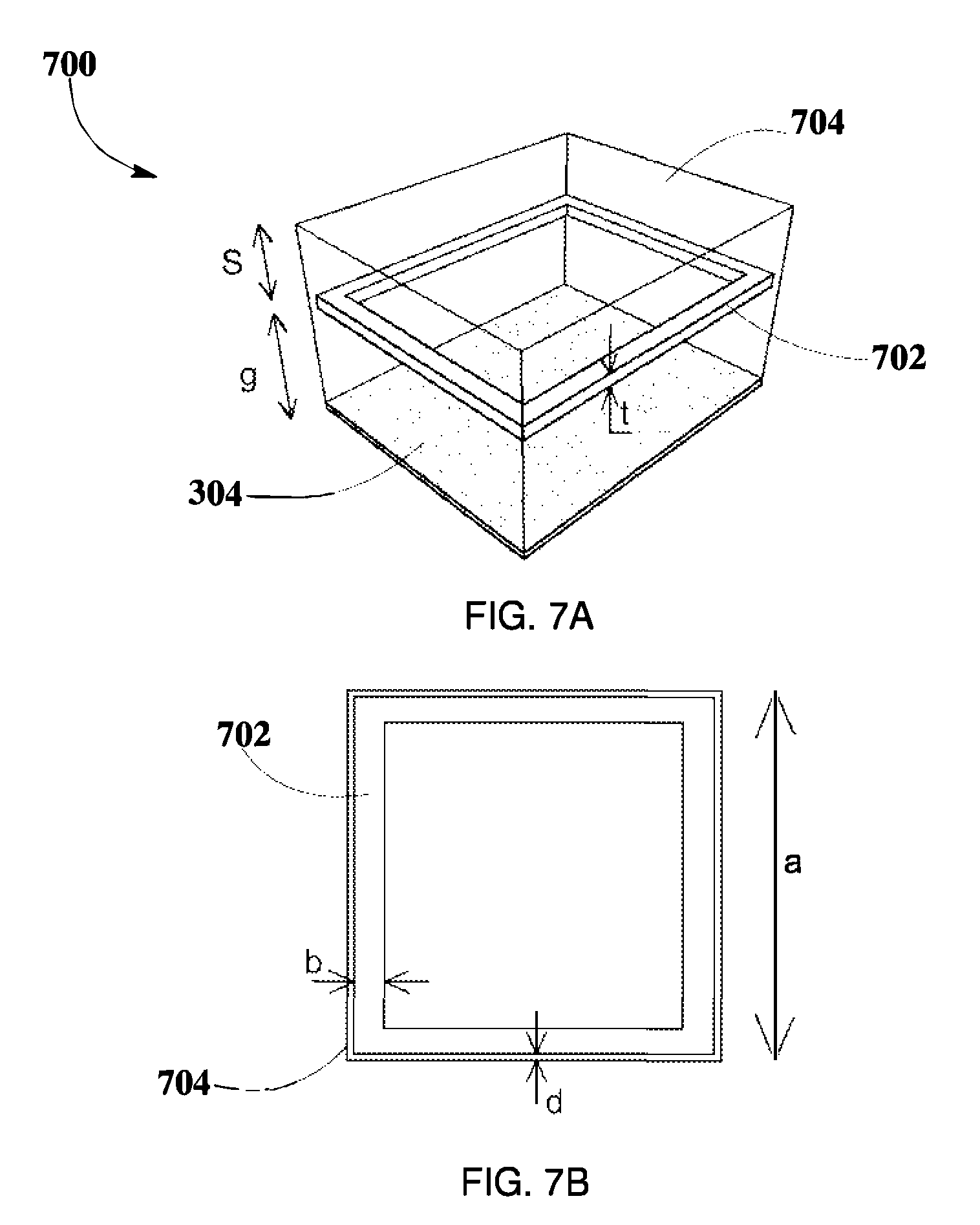
[0033] FIG. 7A shows an isometric view of an AMC unit cell of a metamaterial that may include AMC metal layers resembling a square ring, according to an embodiment.
[0034] FIG. 7B illustrates a top view of the AMC unit cell of an AMC metamaterial, according to an embodiment.
[0035] FIG. 8 illustrates an isometric view of a 6.times.6 array unit cells of an AMC metamaterial that may include AMC metal layers resembling a square ring, according to an embodiment.
[0036] FIG. 9 shows the complex reflection coefficient of an incident plane wave at the surface of an AMC metamaterial that may include AMC metal layers that may resemble a square ring, according to an embodiment.
[0037] FIG. 10 illustrates an isometric view of an exemplary integration of a PIFA with AMC metamaterial that may include an AMC metal layer that may resemble a .theta. square ring, according to an embodiment.
[0038] FIG. 11A illustrates a top view of an exemplary integration of a PIFA with AMC metamaterial that may include an AMC metal layer that may resemble a 0 square ring, according to an embodiment.
[0039] FIG. 11B illustrates a side view of an exemplary integration of a PIFA with AMC metamaterial that may include an AMC metal layer that may resemble a 0 square ring, according to an embodiment.
[0040] FIG. 12A illustrates the impedance bandwidth response of an exemplary integration of a PIFA with AMC metamaterial that may include an AMC metal layer that may resemble a square .theta. ring, according to an embodiment.
[0041] FIG. 12B illustrates the radiation pattern of an exemplary integration of a PTFA with AMC metamaterial that may include an AMC metal layer that may resemble a square .theta. ring, according to an embodiment
[0042] FIG. 13 illustrates an isometric view of an exemplary integration of a PIFA with AMC metamaterial that may include an AMC metal layer that may resemble a square ring, according to an embodiment.
[0043] FIG. 14A illustrates a top view of an exemplary integration of a PIFA with AMC metamaterial that may include an AMC metal layer that may resemble a square ring, according to an embodiment.
[0044] FIG. 14B illustrates a side view of an exemplary integration of a PIFA with AMC metamaterial that may include an AMC metal layer that may resemble a square ring, according to an embodiment
[0045] FIG. 15A illustrates the impedance bandwidth response of an exemplary integration of a PTFA with AMC metamaterial that may include an AMC metal layer that may resemble a square ring, according to an embodiment.
[0046] FIG. 15B illustrates the radiation pattern of all exemplary integration of a PTFA with AMC metamaterial that may include an AMC metal layer that may resemble a square ring, according to an embodiment
DETAILED DESCRIPTION
[0047] The present disclosure is here described in detail with reference to embodiments illustrated in the drawings, which form a part here. Other embodiments may be used and/or other changes may be made without departing from the spirit or scope of the present disclosure. The illustrative embodiments described in the detailed description are not meant to be limiting of the subject matter presented here.
Definitions
[0048] "Pocket-forming" may refer to generating two or more RF waves which converge in 3-d space, forming controlled constructive and destructive interference patterns.
[0049] "Pockets of energy" may refer to areas or regions of space where energy or power may accumulate in the form of constructive interference patterns of RF waves.
[0050] "Null-space" may refer to areas or regions of space where pockets of energy do not form because of destructive interference patterns of RF waves.
[0051] "Transmitter" may refer to a device, including a chip which may generate two or more RF signals, at least one RF signal being phase shifted and gain adjusted with respect to other RF signals, substantially all of which pass through one or more RF antenna such that focused RF signals are directed to a target.
[0052] "Receiver" may refer to a device which may include at least one antenna, at least one rectifying circuit and at least one power converter for powering or charging an electronic device using RF waves.
[0053] "Adaptive pocket-forming" may refer to dynamically adjusting pocket-forming to regulate power on one or more targeted receivers.
[0054] "Metamaterial" a synthetic composite material with a structure such that it exhibits properties not usually found in natural materials. For example naturally occurring materials normally exhibit a positive refraction index for electromagnetic waves. However, fabricated metamaterials may exhibit a negative refractive index.
[0055] "AMC Metamaterial" may refer to an artificial magnetic conductor (AMC) metamaterial that exhibits functionality so that the complex reflection coefficient (S) of a normally incident plane wave, at the material's surface, be S.apprxeq.1. This makes the total electric field, tangential to the material's surface (which is the sum of the incident and reflected electric fields) to be twice as large as the incident field. In contrast, on common metal surfaces (electric conductors), the total field under these conditions is null. More generally, the material exhibits sufficient AMC bandwidth defined as the frequency band where the real part of the complex reflection coefficient is greater than zero (Re {S}.gtoreq.0).
[0056] "AMC Unit cell" may refer to the parts from which an AMC metamaterial may be composed.
DESCRIPTION OF THE DRAWINGS
[0057] In the following detailed description, reference is made to the accompanying drawings, which form a part hereof. In the drawings, which may not be to scale or to proportion, similar symbols typically identify similar components, unless context dictates otherwise. The illustrative embodiments described in the detailed description, drawings and claims, are not meant to be limiting. Other embodiments may be used and/or other changes may be made without departing from the spirit or scope of the present disclosure.
[0058] The present disclosure relates to antennas, and more specifically, to compact and directional planar inverted-F antennas (PIFAs) with metamaterials that may be integrated in antenna arrays for wireless power transmission. An antenna design with small system area may be integrated in artificial magnetic conductor (AMC) metamaterial. The AMC metamaterial may provide the antenna with directionality that may enable the fabrication of compact directional antenna arrays.
[0059] Miniature PIFA Architecture
[0060] FIGS. 1A and 1B illustrate a PIFA 100 with a folded ground 102 that may be formed over the top and bottom layers of a multi-layer printed circuit board (PCB). FIG. 1A shows of an isometric view of PIFA 100 according to embodiments of the present disclosure. FIG. 1B shows a side view of PIFA 100.
[0061] FIG. 1A illustrates an isometric view of PIFA 100 which may be designed to be as small as possible while maintaining suitable performance for wireless power transmission, and it may be formed in a multi-layer printed circuit board (PCB 104) for achieving a monolithic form. In one embodiment, PIFA 100 may be formed on its own PCB 104 which may be connected to the PCB of an electronic device or a transmitter. In another embodiment, several PIFAs 100 may be formed on a large multi-layer PCB that may be part of a transmitter.
[0062] PIFA 100 may include an antenna element 106 formed over the top layer of PCB 104, and a ground element 108 formed over the bottom layer of PCB 104. Both PCB layers may be made of suitable metals such as copper of small metal thickness relative to the total PCB 104 thickness.
[0063] Antenna element 106 may include two antenna slots 110 designed for reducing the area of antenna element 106 while maintaining a suitable bandwidth operation. More antenna slots 110 may be introduced on antenna element 106 for even further area reduction if necessary, according to application.
[0064] Similarly to antenna element 106, ground element 108 may include a ground slot 120 whose main purpose may be reducing the area of the ground element 108 while reducing losses and increasing radiation efficiency.
[0065] PIFA 100 may also include a signal via 112, a ground via 114, and a RF port 116 for electrical connection purposes. In one embodiment, a semi-rigid 50 Ohm coax cable can be connected to RF port 116 for prototype measurements. For integration purposes, PIFA 100 may be fed through RF port 116 by a transmission line integrated in a larger PCB.
[0066] Folded ground 102 on PIFA 100 may be formed over an empty region of PCB 104 top layer without interfering with the performance of antenna clement 106. Folded ground 102 may be raised over the top layer of PCB 104 and may be connected to ground element 108 through folded ground vias 118 which may not significantly affect the performance of PIFA 100. Folded ground 102 may act as an extension of ground element 108.
[0067] According to some aspects of this embodiment, folded ground 102 may allow to reduce the dimensions of PIFA 100. PIFA 100 dimensions in the x-axis, y-axis, and z-axis may be about 10 mm, 3 0 mm, and 2 4 mm respectively, for a system area of about 30 mm.sup.2 and a system volume of about 72 mm.sup.3.
[0068] FIG. 1B illustrates a side view of PIFA 100 where folded ground 102 and antenna element 106 may be formed on top of PCB 104. Ground element 108 may be formed on the bottom of PCB 104. Folded ground vias 118, signal via 112, and ground via 114 are also shown in FIG. 1B.
[0069] FIGS. 2A and 2B show an omnidirectional isometric radiation pattern 200 of PIFA 100 (as oriented in FIGS. 1A and 1B). This omnidirectional radiation pattern in FIG. 2A may be similar to radiation patterns exhibited in dipole antennas, thereby allowing flexible placement or integration of PIFA into larger form factors systems or PCBs. In one embodiment, PTFA 100 may exhibit a maximum gain of about +0.49 dBi at 5.8 GHz.
[0070] FIG. 2B illustrates the return loss of PIFA 100 when fed by a 50-Ohm port. As seen from probes m1 and m2, PIFA 100 may exhibit an impedance bandwidth of about 210 MHz at -10 dB, where this bandwidth may provide sufficient margins for possible detuning upon integration of PIFA into an electronic device or a larger PCB. Radiation efficiency of PIFA may be around 80% at about 5.8 GHz.
[0071] Although PIFA 100 may exhibit suitable characteristics for wireless power transmission, it may be an object of the following embodiments to provide integrated antenna structures with a similar monolithic PCB form factor, and performance in terms of bandwidth and radiation efficiency, but with a directional radiation pattern suitable for transmission of focused RF waves.
[0072] AMC Unit Cells and AMC Unit Cell Arrays
[0073] FIG. 3 illustrates a side view of an exemplary embodiment of an AMC unit cell 300 of an AMC metamaterial in which PIFA 100 may be integrated. AMC Unit cell 300 may include an AMC metal layer 302, a backing metal layer 304. AMC Unit cell 300 may be formed in a multi-layer printed circuit board (PCB 306) for achieving a monolithic form. Edge 308 of AMC unit cell 300 may be close to AMC metal layer 302 but not coincident to edge 308 of AMC metal layer 302. In one embodiment, several AMC unit cells 300 of an AMC metamaterial may be formed on a larger multi-layer PCB.
[0074] A large variety of elements design in an AMC unit cell 300 may be realized on a multi-layer PCB 306 that may fulfill the required functionality of an AMC metamaterial. Arrays of AMC unit cells 300 may additionally be integrated with PIFAs; two exemplary designs are illustrated and listed in the following description.
[0075] First AMC Unit Cell Exemplary Embodiment
[0076] FIGS. 4A and 4B illustrate an exemplary design of an AMC unit cell 400 according to an embodiment. FIG. 4A illustrates an isometric view of AMC unit cell 400, while FIG. 4B illustrates a top-view of AMC unit cell 400.
[0077] FIG. 4A illustrates an isometric view of AMC unit cell 400 that may include an AMC metal layer 402 and backing metal layer 304. AMC metal layer 402 may exhibit a square 0 ring shape, and may be formed on at least one inner layer of a multi-layer PCB 404. Backing metal layer 304 may be formed on another layer of PCB 404.
[0078] Dimensions of AMC unit cell 400 illustrated in FIG. 4A may be about 0.06 mm, 0.887 mm, and 1.453 mm for t, s, and g, respectively.
[0079] A side view of AMC unit cell 400 is illustrated in FIG. 4B. Distance (d) between outer edge of AMC unit cell 400 and outer edge of AMC metal layer 402 may be about 0.0425 mm. Dimensions of AMC metal layer 402 illustrated in FIG. 4B may be about 0.276 mm, 0.135 mm, and 3.581 mm for b, c, and a, respectively.
[0080] These dimensions as well as the shape exhibited by AMC metal layer 402 may determine the frequency tuning and bandwidth of AMC unit cell 400 functionality.
[0081] First AMC Metamaterial Exemplary Embodiment
[0082] FIG. 5 illustrates an exemplary embodiment of a first AMC metamaterial 500. AMC metamaterial 500 may exhibit a configuration of 5.times.5 array of AMC unit cells 400. AMC unit cells 400 in AMC metamaterial 500 may include AMC metal layer 402 and backing metal layer 304. AMC metamaterial 500 may be formed over a large monolithic multi-layer PCB 502 to fit a plurality of AMC unit cells 400. According to some aspects of this embodiment, AMC metamaterial 500 may exhibit the properties of an AMC metamaterial.
[0083] FIG. 6 illustrates the complex reflection coefficient graph 600 of AMC metamaterial 500 computed on its top surface, under normal plane wave incidence on a laterally infinite 2-dimensional artificial crystal. The real part of the reflection coefficient may have the property Re {S}.gtoreq.0 in the frequency range of about 5.15 to about 6.05 GHz, for an estimated bandwidth of about 900 MHz. AMC metamaterial 500 may be tuned to a resonant frequency of about 5.65 GHz which may be designed to be the low-band edge of a desired impedance-matched frequency band. The corresponding value of the complex reflection coefficient for AMC metamaterial 500 at a resonant frequency of 5.65 GHz may be S=0.9+j0.
[0084] In one embodiment, AMC unit cell 400 dimensions may be about 0.068.times.0.068.times.0.046.lamda..sup.3, where .lamda. may be the wavelength at the resonant frequency of the AMC unit cell 400. These dimensions exhibited by AMC unit cell 400 may be suitable for integration with small PIFAs such as PIFA 100. A plurality of AMC unit cells 400 may be required to recreate a metamaterial that may impose AMC functionality to an antenna such as PIFA 100.
[0085] Second AMC Unit Cell Exemplary Design
[0086] FIGS. 7A and 7B illustrate an exemplary design of an AMC unit cell 700, according to an embodiment. FIG. 7A illustrates an isometric view of AMC unit cell 700, while FIG. 7B illustrates a top-view of AMC unit cell 700.
[0087] FIG. 7A illustrates an isometric view of an AMC unit cell 700 that may include all AMC metal layer 702 and backing metal layer 304. AMC metal layer 702 may exhibit a square ring shape and may be formed on one of the inner layers of a multi-layer PCB 704. Backing metal layer 304 may be formed on another layer of PCB 704.
[0088] Dimensions of AMC unit cell 700 illustrated in FIG. 7A may be about 0.06 mm, 0.887 mm, and 1.453 for t, s, and g, respectively.
[0089] A top view of AMC unit cell 700 is illustrated in FIG. 7B where distance (d) between outer edge of AMC unit cell 700 and outer edge of AMC metal layer 702 may be about 0.04 mm. Additionally, the dimensions of AMC metal layer 702 may be about 0.23 mm, and 3 0 mm for b, and a, respectively.
[0090] Second AMC Metamaterial Exemplary Embodiment
[0091] FIG. 8 illustrates an exemplary embodiment of a second AMC metamaterial 800. AMC metamaterial 800 may exhibit a configuration of 6.times.6 array of AMC unit cells 700. AMC unit cells 700 in AMC metamaterial 800 may include AMC metal layer 702 and backing metal layer 304. AMC metamaterial 800 may be formed over a large monolithic multi-layer PCB 802 to fit a plurality of AMC unit cells 700. According to some aspects of this embodiment, AMC metamaterial 800 may exhibit the properties of an AMC metamaterial.
[0092] FIG. 9 illustrates the complex reflection coefficient response 900 of AMC metamaterial 800 computed on its top surface, under normal plane wave incidence on a laterally infinite 2-dimensional artificial crystal. The real part of the reflection coefficient may have the property Re {S}.gtoreq.0 in the frequency range of about 5.25 to about 6.1 GHz, for an estimated bandwidth of about 850 MHz. AMC metamaterial 800 may be tuned to a resonant frequency of about 5.7 GHz which may be designed to be the low-band edge of a desired impedance-matched frequency band. The corresponding value of the complex reflection coefficient for AMC metamaterial 800 at a resonant frequency of 5.7 GHz may be S=0.9+j0.
[0093] In one embodiment, AMC unit cell 700 dimensions may be about 0.057.times.0.057.times.0.046.lamda..sup.3, where .lamda. may be the wavelength at the resonant frequency of the AMC unit cell 700. These dimensions exhibited by AMC unit cell 700 may be suitable for integration with small PIFAs such as PIFA 100. A plurality of AMC unit cells 700 may be required to recreate a metamaterial that may impose AMC functionality to an antenna such as PIFA 100.
[0094] Integrated Antenna Structures
[0095] PIFA and AMC metamaterial integration may be realized on a multi-layer PCB that may fulfill the required functionality of a directional antenna; two exemplary embodiments of integrated antenna structures are illustrated and described below, where these integrated antenna structures may be part of a transmitter device configured for sending focused RF waves towards a receiver for wireless charging or powering.
[0096] Integrated Antenna Structure Including PIFA+First AMC Metamaterial
[0097] FIG. 10 illustrates an isometric view of an exemplary integrated antenna structure 1000 that may include first AMC metamaterial 500 integrated with PIFA 100.
[0098] Integrated antenna structure 1000 may include a monolithic four layer PCB 1002 that may be used as a substrate to suitably integrate AMC metamaterial 500 with PIFA 100. For example, antenna element 106 and folded ground 102 of PIFA 100 may be formed on the top layer of PCB 1002; AMC metal layer 402 of AMC metamaterial 500 may be formed in one of the inner layers of PCB 1002; Backing metal layer 304 of AMC metamaterial 500 may be formed on the other available inner layer of PCB 1002; and ground element 108 of PTFA 100 may be formed on the bottom layer of PCB 1002.
[0099] A hole 1004 may be formed in backing metal layer 304 for allowing signal via 112 and ground via 114 to pass through backing metal layer 304 without electrically shortening it. As a result, ground element 108 of PIFA 100 shorted with backing metal layer 304 may become the primary ground of the integrated antenna structure 1000. At the opposite ends of this primary ground, folded ground vias 118 may short-circuit backing metal layer 304 at a crossing point. In another embodiment where PIFA 100 has no folded ground 102, folded ground vias 118 may be also formed to electrically short backing metal layer 304 and ground element 108.
[0100] In other embodiments, PIFA 100 may have different dimensions and configurations than those described in FIGS. 1A and 1B.
[0101] FIGS. 11A and 11B illustrate top and side views of integrated antenna structure 1000. In some embodiments, as illustrated in FIG. 11A, PIFA 100 may occupy about three AMC unit cells 400 of the AMC metamaterial 500 formed on PCB 1002. In some embodiments as illustrated in FIG. 11A, integrated antenna structure 1000 may include dimensions of about 18 mm and 18 mm form and n respectively, for a system area of about 324 mm.sup.2.
[0102] FIG. 11B shows a side view of integrated antenna structure 1000 where it may be noticed how the AMC metamaterial 500 is integrated with PIFA 100. As shown in FIG. 11B, antenna element 106 and folded ground 102 may be formed on top side of PCB 1002, while ground element 108 may be formed on the bottom side of PCB 1002. Backing metal layer 304 and AMC metal layer 402 may be formed in the inner layers of PCB 1002, between antenna element 106 and ground element 108. Folded ground vias 118, signal via 112, and ground via 114 are also illustrated in FIG. 11B according to embodiments described herein. Thickness h of integrated antenna structure 1000 may be about 2.4 mm.
[0103] Overall dimensions for integrated antenna structure 1000 may vary according to the dimensions used for the AMC unit cells 400 and PIFA 100, as well as the desired application.
[0104] FIGS. 12A and 12B illustrate the return loss and radiation pattern 1200 of exemplary integrated antenna structure 1000 when fed by a 50-Ohm port. As shown in FIG. 12A, integrated antenna structure 1000 may exhibit an impedance bandwidth of about 160 MHz at -10 dB, where this bandwidth may provide sufficient margins for possible detuning upon integration of the exemplary integrated antenna structure 1000 into an electronic device or a larger PCB. Radiation efficiency of integrated antenna structure 1000 may be of about 72% at 5.8 GHz. The 8% point-drop from the efficiency of PIFA 100 may be due to the integration of the AMC metamaterial 500, specifically the addition of the metallization layers, AMC metal layer 302 and backing metal layer 304.
[0105] FIG. 12B illustrates the radiation pattern of integrated antenna structure 1000, where the maximum gain may be of about 2.2 dBi at 5.8 GHz. Integrated antenna structure 1000 may exhibit a directional radiation pattern, more specifically, a directional broadside pattern that may be about twice of that of the omnidirectional radiation pattern exhibited by PIFA 100 in FIGS. 2A and 2B. In this way, by integrating the AMC metamaterial 500 with PIFA 100 in the integrated antenna structure 1000, the omnidirectional pattern of PIFA 100 may be changed to a directional pattern as exhibited in FIG. 12B, where the AMC metamaterial 500 may operate as an artificial magnetic reflector, sending all the energy upwards. Still, the overall dimensions of integrated antenna structure 1000 may be about 0.345.times.0.345.times.0.05.lamda..sup.3 which may significantly smaller compared to conventional directional antennas such as a half-wave conductor-backed dipole. For example, a half-wave center-fed linear dipole with a quarter-wave backing metal reflector may need a system size of at least 0.5.times.0.5.times.0.25.lamda..sup.3 to achieve a similar performance of integrated antenna structure 1000.
[0106] Integrated Antenna Structure Including PIFA+Second AMC Metamaterial Embodiment
[0107] FIG. 13 illustrates an isometric view of an exemplary integrated antenna structure 1300 that may include second AMC metamaterial 800 integrated with PIFA 100.
[0108] Integrated antenna structure 1300 may include a monolithic four layer PCB 1302 that may be used as a substrate to suitably integrate AMC metamaterial 800 with PIFA 100. For example, antenna element 106 and folded ground 102 of PIFA 100 may be formed on the top layer of PCB 1302; AMC metal layer 702 of AMC metamaterial 800 may be formed in one of the inner layers of PCB 1302; Backing metal layer 304 of AMC metamaterial 800 may be formed on the other available inner layer of PCB 1302; and ground element 108 of PIFA 100 may be formed on the bottom layer of PCB 1302.
[0109] A hole 1304 may be formed in backing metal layer 304 for allowing signal via 112 and ground via 114 to pass through backing metal layer 304 without electrically shortening it. As a result, ground element 108 of PIFA 100 shorted with backing metal layer 304 may become the primary ground of the integrated antenna structure 1300. At the opposite ends of this primary ground, folded ground vias 118 may short-circuit backing metal layer 304 at a crossing point. In another embodiment where PIFA 100 has no folded ground 102, folded ground vias 118 may be also formed to electrically short backing metal layer 304 and ground element 108.
[0110] In other embodiments, PIFA 100 may have different dimensions and configurations than those described in FIGS. 1A and 1B.
[0111] FIGS. 14A and 14B illustrate top and side views of integrated antenna structure 1300. In some embodiments, as illustrated in FIG. 14A, PIFA 100 may occupy about eight AMC unit cells 700 of the AMC metamaterial 800 formed on PCB 1302. In some embodiments as illustrated in FIG. 14A, integrated antenna structure 1300 may include dimensions of about 18 mm and 18 mm form and n respectively, for a system area of about 324 mm.sup.2.
[0112] FIG. 14B shows a side view of integrated antenna structure 1300 where it may be noticed how the AMC metamaterial 800 is integrated with PIFA 100. As shown in FIG. 14B, antenna element 106 and folded ground 102 may be formed on top side of PCB 1302, while ground element 108 may be formed on the bottom side of PCB 1302. Backing metal layer 304 and AMC metal layer 702 may be formed in the inner layers of PCB 1302, between antenna element 106 and ground element 108. Folded ground vias 118, signal via 112, and ground via 114 are also illustrated in FIG. 14B according to embodiments described herein. Thickness h of integrated antenna structure 1300 may be about 2.4 mm.
[0113] Overall dimensions for integrated antenna structure 1300 may vary according to the dimensions used for the AMC unit cells 700 and PIFA 100, as well as the desired application.
[0114] FIGS. 15A and 15B illustrate the return loss and radiation pattern 1500 of exemplary integrated antenna structure 1300 when fed by a 50-Ohm port. As shown in FIG. 15A, integrated antenna structure 1300 may exhibit an impedance bandwidth of about 160 MHz at -10 dB, where this bandwidth may provide sufficient margins for possible detuning upon integration of the exemplary integrated antenna structure 1300 into an electronic device or a larger PCB. Radiation efficiency of integrated antenna structure 1300 may be of about 67% at 5.8 GHz. The 13% point-drop from the efficiency of PIFA 100 may be due to the integration of the AMC metamaterial 800, specifically the addition of the metallization layers, AMC metal layer 702 and backing metal layer 304, configured in a larger 6.times.6 array compared to the 5.times.5 array configured in AMC metamaterial 500, hence the larger amount of AMC metallization and radiation efficiency degradation.
[0115] FIG. 15B illustrates the radiation pattern of integrated antenna structure 1300, where the maximum gain may be of about 2.0 dBi at 5.8 GHz. Integrated antenna structure 1300 may exhibit a directional radiation pattern, more specifically a directional broadside pattern that may be about twice of that of the omnidirectional radiation pattern exhibited by PIFA 100 in FIGS. 2A and 2B. In this way, by integrating the AMC metamaterial 800 with PIFA 100 in the integrated antenna structure 1300, the omnidirectional pattern of PIFA 100 may be changed to a directional pattern as exhibited in FIG. 15B, where the AMC metamaterial 800 may operate as an artificial magnetic reflector, sending all the energy upwards. Still, the overall dimensions of integrated antenna structure 1300 may be about 0.345.times.0.345.times.0.05.lamda..sup.3 which may significantly smaller compared to conventional directional antennas such as a half-wave conductor-backed dipole. For example, a half-wave center-fed linear dipole with a quarter-wave backing metal reflector may need a system size of at least 0.5.times.0.5.times.0.25 to achieve a similar performance of integrated antenna structure 1300.
[0116] The embodiments of integrated antenna structures 1000, 1300 featuring the integration of first AMC metamaterial 500 and second AMC metamaterial 800 with PIFA 100 may suggest that as long as the two metamaterials may exhibit a similar response as shown in FIG. 6 and FIG. 9, the integration of PIFAs with metamaterials described herein may be robust and may lead to similar results as shown in FIGS. 12A and 12B and FIGS. 15A and 15B.
[0117] While various aspects and embodiments have been disclosed herein, other aspects and embodiments are contemplated. The various aspects and embodiments disclosed herein are for purposes of illustration and are not intended to be limiting, with the true scope and spirit being indicated by the following claims.
* * * * *
D00000
D00001
D00002
D00003
D00004
D00005
D00006
D00007
D00008
D00009
D00010
D00011
D00012

D00013

D00014

D00015

XML
uspto.report is an independent third-party trademark research tool that is not affiliated, endorsed, or sponsored by the United States Patent and Trademark Office (USPTO) or any other governmental organization. The information provided by uspto.report is based on publicly available data at the time of writing and is intended for informational purposes only.
While we strive to provide accurate and up-to-date information, we do not guarantee the accuracy, completeness, reliability, or suitability of the information displayed on this site. The use of this site is at your own risk. Any reliance you place on such information is therefore strictly at your own risk.
All official trademark data, including owner information, should be verified by visiting the official USPTO website at www.uspto.gov. This site is not intended to replace professional legal advice and should not be used as a substitute for consulting with a legal professional who is knowledgeable about trademark law.