Pixel Circuits For Amoled Displays
Chaji; Gholamreza
U.S. patent application number 16/177353 was filed with the patent office on 2019-03-07 for pixel circuits for amoled displays. The applicant listed for this patent is Ignis Innovation Inc.. Invention is credited to Gholamreza Chaji.
| Application Number | 20190073958 16/177353 |
| Document ID | / |
| Family ID | 50880459 |
| Filed Date | 2019-03-07 |


View All Diagrams
| United States Patent Application | 20190073958 |
| Kind Code | A1 |
| Chaji; Gholamreza | March 7, 2019 |
PIXEL CIRCUITS FOR AMOLED DISPLAYS
Abstract
A system is provided for controlling an array of pixels in a display in which each pixel includes a light-emitting device and a reference voltage source that controllably supplies a reference voltage having a magnitude that turns off the light-emitting device. While the reference voltage is coupled to a drive transistor, a control voltage is supplied to the gate of the drive transistor to cause the drive transistor to transfer to a node common to the drive transistor and the light-emitting device, a voltage that is a function of the threshold voltage and mobility of the drive transistor. During an emission cycle, the current conveyed through the light emitting device via the drive transistor is controlled by a voltage stored in the storage capacitor, which is a function of the threshold voltage and mobility of the drive transistor so that the current supplied to the light-emitting device remains stable.
| Inventors: | Chaji; Gholamreza; (Waterloo, CA) | ||||||||||
| Applicant: |
|
||||||||||
|---|---|---|---|---|---|---|---|---|---|---|---|
| Family ID: | 50880459 | ||||||||||
| Appl. No.: | 16/177353 | ||||||||||
| Filed: | October 31, 2018 |
Related U.S. Patent Documents
| Application Number | Filing Date | Patent Number | ||
|---|---|---|---|---|
| 15703357 | Sep 13, 2017 | 10140925 | ||
| 16177353 | ||||
| 13710872 | Dec 11, 2012 | 9786223 | ||
| 15703357 | ||||
| Current U.S. Class: | 1/1 |
| Current CPC Class: | G09G 2320/0295 20130101; G09G 2300/0861 20130101; G09G 2320/0693 20130101; G09G 2300/0842 20130101; G09G 2300/0819 20130101; G09G 3/3233 20130101; G09G 2300/0408 20130101; G09G 3/3291 20130101; G09G 2330/10 20130101; G09G 3/3258 20130101 |
| International Class: | G09G 3/3258 20060101 G09G003/3258; G09G 3/3233 20060101 G09G003/3233; G09G 3/3291 20060101 G09G003/3291 |
Claims
1-10. (canceled)
11. A display system comprising: a reference voltage source; a supply voltage source; and a plurality of pixels, each pixel comprising a pixel circuit including: a light-emitting device, a drive transistor for driving current through the light emitting device according to a driving voltage across the drive transistor during an emission cycle, said drive transistor having a gate and a threshold voltage, a storage capacitor coupled to said drive transistor for storing said driving voltage, and a reference voltage transistor coupled to the reference voltage source for coupling the drive transistor to the reference voltage source during a first operation cycle for charging a node common to said storage capacitor and coupled to said drive transistor to the reference voltage, the reference voltage transistor for isolating the drive transistor from the reference voltage source during a second operation cycle subsequent to the first operation cycle for allowing said drive transistor to transfer to said node, a voltage that is a function of the threshold voltage and mobility of said drive transistor.
12. The display system of claim 11 in which said voltage stored in said storage capacitor is a function of the threshold voltage and mobility of said drive transistor so that the current supplied to said light-emitting device remains stable.
13. The display system of claim 11 in which said voltage stored in said storage capacitor is the difference between a programming voltage and said reference voltage.
14. The display system of claim 11 in which said storage capacitor is connected across the drive transistor
15. The display system of claim 11 which includes a data line controllably coupled to said drive transistors of said pixel circuits for programming the pixel circuits with driving voltages, and a controller coupled to said pixel circuits and adapted to receive a data input indicative of an amount of luminance to be emitted from the light-emitting device in each of said pixel circuits, receive an indication of the amount of degradation of at least one of said drive transistor and said light-emitting device in each of said pixel circuits, and determine an amount of compensation to provide to each pixel circuit based on said amount of degradation.
16. The display system of claim 15 which includes a monitor line for extracting a voltage or a current indicative of said amount of degradation in each of said pixel circuits.
17. The display system of claim 11 wherein each said pixel circuit further includes a switching transistor coupled to a gate of said drive transistor for supplying a control voltage to the gate of said drive transistor during the first operation cycle for causing said drive transistor to charge said node to said reference voltage, the gate of the switching transistor coupled to a select line.
18. The display system of claim 11 wherein said reference voltage has a magnitude that turns off said light-emitting device during the first operation cycle.
19. The display system of claim 11 wherein the reference voltage transistor is coupled to said node.
20. The display system of claim 11 wherein each said pixel circuit further includes a switching transistor coupled to a gate of said drive transistor for supplying a control voltage to the gate of said drive transistor during said second operation cycle for causing said drive transistor to transfer to said node said voltage that is a function of the threshold voltage and mobility of said drive transistor.
21. The display system of claim 11 wherein each said pixel circuit further includes an emission transistor arranged to couple, during said emission cycle, said supply voltage source to said drive transistor such that current is conveyed through said light emitting device via said drive transistor, said current being controlled by said voltage stored in said storage capacitor, said emission transistor arranged to couple, during the second operation cycle, said supply voltage source to said drive transistor such that said voltage that is a function of the threshold voltage and mobility of said drive transistor is transferred to said node via said drive transistor.
22. The display system of claim 11 wherein the node is common to said storage capacitor and said drive transistor.
23. The display system of claim 21 wherein each said pixel circuit further includes a reset transistor coupled to a reset line, the reset transistor for controlling a coupling of said reset line to the gate of said drive transistor prior to or during the first operation cycle, and wherein said node is charged to said reference voltage during the first operation cycle for turning on said drive transistor without turning on said light-emitting device.
24. The display system of claim 1 wherein the supply voltage source is coupled to said drive transistor such that current is conveyed through said light-emitting device via said drive transistor during the emission cycle, said current being controlled by the voltage stored in said storage capacitor, wherein the node is common to said storage capacitor, said light emitting device, and said drive transistor, the node charged to said reference voltage for turning on said drive transistor without turning on said light-emitting device.
Description
FIELD OF THE INVENTION
[0001] The present disclosure generally relates to circuits for use in displays, and methods of driving, calibrating, and programming displays, particularly displays such as active matrix organic light emitting diode displays.
BACKGROUND
[0002] Displays can be created from an array of light emitting devices each controlled by individual circuits (i.e., pixel circuits) having transistors for selectively controlling the circuits to be programmed with display information and to emit light according to the display information. Thin film transistors ("TFTs") fabricated on a substrate can be incorporated into such displays. TFTs tend to demonstrate non-uniform behavior across display panels and over time as the displays age. Compensation techniques can be applied to such displays to achieve image uniformity across the displays and to account for degradation in the displays as the displays age.
[0003] Some schemes for providing compensation to displays to account for variations across the display panel and over time utilize monitoring systems to measure time dependent parameters associated with the aging (i.e., degradation) of the pixel circuits. The measured information can then be used to inform subsequent programming of the pixel circuits so as to ensure that any measured degradation is accounted for by adjustments made to the programming. Such monitored pixel circuits may require the use of additional transistors and/or lines to selectively couple the pixel circuits to the monitoring systems and provide for reading out information. The incorporation of additional transistors and/or lines may undesirably decrease pixel-pitch (i.e., "pixel density").
SUMMARY
[0004] In accordance with one embodiment, a system is provided for controlling an array of pixels in a display in which each pixel includes a light-emitting device and a pixel circuit that has a drive transistor for driving current through the light emitting device according to a driving voltage across the drive transistor during an emission cycle, and a storage capacitor coupled to the drive transistor for controlling the driving voltage. A reference voltage source is coupled to a reference voltage transistor that controls the coupling of the reference voltage source to the drive transistor, to supply a reference voltage having a magnitude that turns off the light-emitting device. A switching transistor is coupled to the gate of the drive transistor for supplying a control voltage to the gate of the drive transistor while the reference voltage is coupled to the drive transistor, to cause the drive transistor to transfer to a node common to the drive transistor and the light-emitting device, a voltage that is a function of the threshold voltage and mobility of the drive transistor. A supply voltage source is coupled to an emission transistor arranged to couple, during the emission cycle, the supply voltage source to the drive transistor such that current is conveyed through the light emitting device via the drive transistor, the current being controlled by a voltage stored in the storage capacitor. In one implementation, the voltage stored in the storage capacitor is a function of the threshold voltage and mobility of the drive transistor so that the current supplied to the light-emitting device remains stable. For example, the voltage stored in the storage capacitor may be the difference between a programming voltage and the reference voltage.
[0005] The system may include a data line controllably coupled to the drive transistors of the pixel circuits for programming the pixel circuits with driving voltages, and a controller coupled to the pixel circuits and adapted to (1) receive a data input indicative of an amount of luminance to be emitted from the light-emitting device in each of the pixel circuits, (2) receive an indication of the amount of degradation of at least one of the drive transistor and the light-emitting device in each of the pixel circuits, and (3) determine an amount of compensation to provide to each pixel circuit based on the amount of degradation. A monitor line may be included for extracting a voltage or a current indicative of the amount of degradation in each of the pixel circuits.
[0006] In another embodiment, each pixel circuit includes a drive transistor for driving current through the light emitting device according to a driving voltage across the drive transistor during a drive cycle, a storage capacitor coupled to the drive transistor for controlling the driving voltage, a reset line coupled to a reset voltage transistor that controls the coupling of the reset line to the gate of the drive transistor, a monitor line coupled to a monitor transistor that controls the coupling of a calibration voltage to a node common to the storage capacitor, the light-emitting device and the drive transistor for turning on the drive transistor without turning on the light-emitting device, while the reset line is coupled to the drive transistor, thereby charging the node to a voltage that is a function of the threshold voltage, mobility and other parameters of the drive transistor and thus compensates for changes in the threshold voltage, mobility and other parameters over time. A supply voltage source is coupled to the drive transistor such that current is conveyed through the light-emitting device via the drive transistor during a drive cycle, the current being controlled by a voltage stored in the storage capacitor, and a switching transistor is coupled to the gate of the drive transistor for supplying a programming voltage to the storage capacitor while the calibration transistor and the reset transistor are turned off.
[0007] The foregoing and additional aspects and embodiments of the present invention will be apparent to those of ordinary skill in the art in view of the detailed description of various embodiments and/or aspects, which is made with reference to the drawings, a brief description of which is provided next.
BRIEF DESCRIPTION OF THE DRAWINGS
[0008] The foregoing and other advantages of the invention will become apparent upon reading the following detailed description and upon reference to the drawings.
[0009] FIG. 1 illustrates an exemplary configuration of a system for driving an OLED display while monitoring the degradation of the individual pixels and providing compensation therefor.
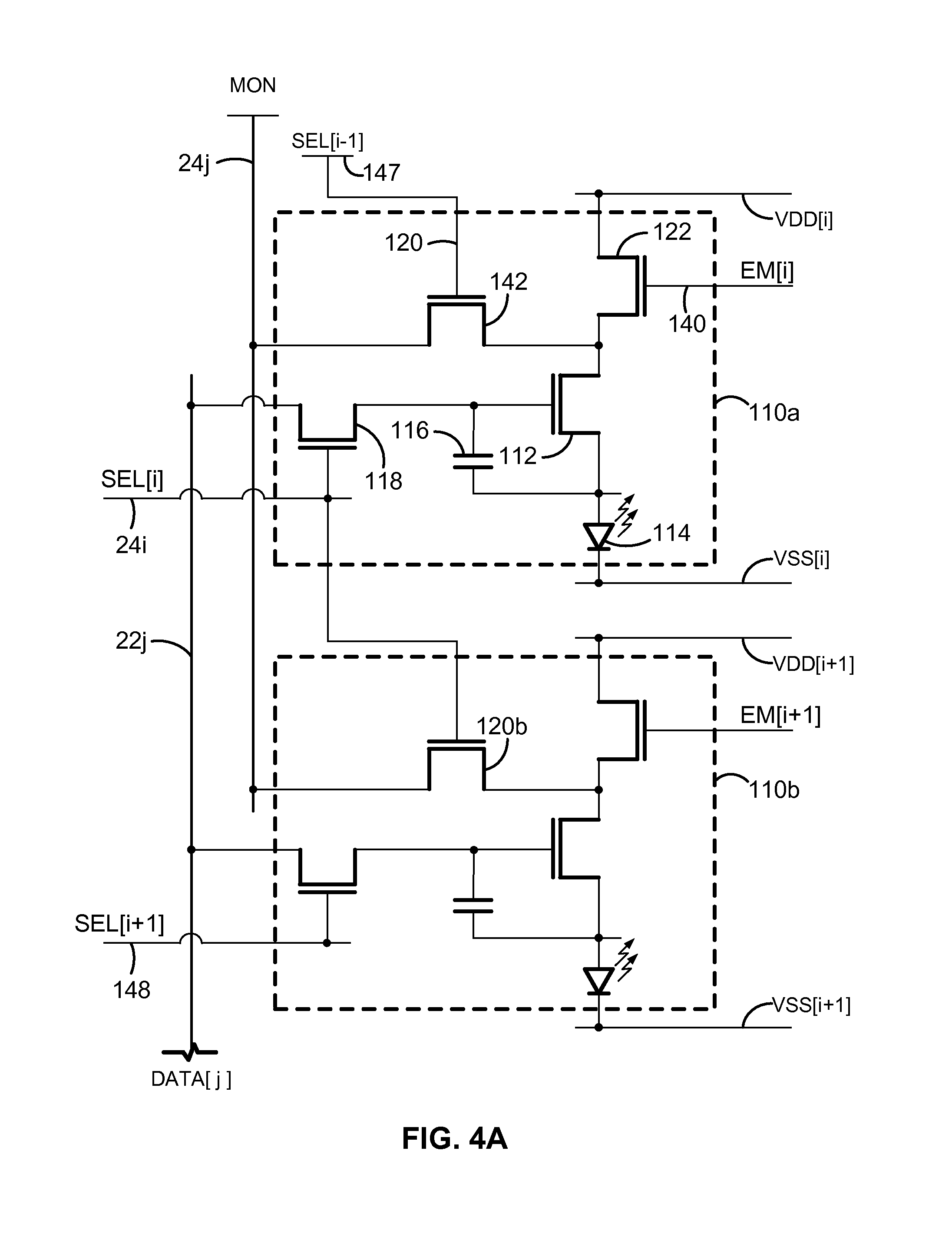
[0010] FIG. 2A is a circuit diagram of an exemplary pixel circuit configuration.
[0011] FIG. 2B is a timing diagram of first exemplary operation cycles for the pixel shown in FIG. 2A.
[0012] FIG. 2C is a timing diagram of second exemplary operation cycles for the pixel shown in FIG. 2A.
[0013] FIG. 3A is a circuit diagram of an exemplary pixel circuit configuration.
[0014] FIG. 3B is a timing diagram of first exemplary operation cycles for the pixel shown in FIG. 3A.
[0015] FIG. 3C is a timing diagram of second exemplary operation cycles for the pixel shown in FIG. 3A.
[0016] FIG. 4A is a circuit diagram of an exemplary pixel circuit configuration.
[0017] FIG. 4B is a circuit diagram of a modified configuration for two identical pixel circuits in a display.
[0018] FIG. 5A is a circuit diagram of an exemplary pixel circuit configuration.
[0019] FIG. 5B is a timing diagram of first exemplary operation cycles for the pixel illustrated in FIG. 5A.
[0020] FIG. 5C is a timing diagram of second exemplary operation cycles for the pixel illustrated in FIG. 5A.
[0021] FIG. 5D is a timing diagram of third exemplary operation cycles for the pixel illustrated in FIG. 5A.
[0022] FIG. 5E is a timing diagram of fourth exemplary operation cycles for the pixel illustrated in FIG. 5A.
[0023] FIG. 5F is a timing diagram of fifth exemplary operation cycles for the pixel illustrated in FIG. 5A.
[0024] FIG. 6A is a circuit diagram of an exemplary pixel circuit configuration.
[0025] FIG. 6B is a timing diagram of exemplary operation cycles for the pixel illustrated in FIG. 6A.
[0026] FIG. 7A is a circuit diagram of an exemplary pixel circuit configuration.
[0027] FIG. 7B is a timing diagram of exemplary operation cycles for the pixel illustrated in FIG. 7A.
[0028] FIG. 8A is a circuit diagram of an exemplary pixel circuit configuration.
[0029] FIG. 8B is a timing diagram of exemplary operation cycles for the pixel illustrated in FIG. 8A.
[0030] FIG. 9A is a circuit diagram of an exemplary pixel circuit configuration.
[0031] FIG. 9B is a timing diagram of first exemplary operation cycles for the pixel illustrated in FIG. 9A.
[0032] FIG. 9C is a timing diagram of second exemplary operation cycles for the pixel illustrated in FIG. 9A.
[0033] FIG. 10A is a circuit diagram of an exemplary pixel circuit configuration.
[0034] FIG. 10B is a timing diagram of exemplary operation cycles for the pixel illustrated in FIG. 10A in a programming cycle.
[0035] FIG. 10C is a timing diagram of exemplary operation cycles for the pixel illustrated in FIG. 10A in a TFT read cycle.
[0036] FIG. 10D is a timing diagram of exemplary operation cycles for the pixel illustrated in FIG. 10A in am OLED read cycle.
[0037] While the invention is susceptible to various modifications and alternative forms, specific embodiments have been shown by way of example in the drawings and will be described in detail herein. It should be understood, however, that the invention is not intended to be limited to the particular forms disclosed. Rather, the invention is to cover all modifications, equivalents, and alternatives falling within the spirit and scope of the invention as defined by the appended claims.
DETAILED DESCRIPTION
[0038] FIG. 1 is a diagram of an exemplary display system 50. The display system 50 includes an address driver 8, a data driver 4, a controller 2, a memory storage 6, and display panel 20. The display panel 20 includes an array of pixels 10 arranged in rows and columns. Each of the pixels 10 are individually programmable to emit light with individually programmable luminance values. The controller 2 receives digital data indicative of information to be displayed on the display panel 20. The controller 2 sends signals 32 to the data driver 4 and scheduling signals 34 to the address driver 8 to drive the pixels 10 in the display panel 20 to display the information indicated. The plurality of pixels 10 associated with the display panel 20 thus comprise a display array ("display screen") adapted to dynamically display information according to the input digital data received by the controller 2. The display screen can display, for example, video information from a stream of video data received by the controller 2. The supply voltage 14 can provide a constant power voltage or can be an adjustable voltage supply that is controlled by signals from the controller 2. The display system 50 can also incorporate features from a current source or sink (not shown) to provide biasing currents to the pixels 10 in the display panel 20 to thereby decrease programming time for the pixels 10.
[0039] For illustrative purposes, the display system 50 in FIG. 1 is illustrated with only four pixels 10 in the display panel 20. It is understood that the display system 50 can be implemented with a display screen that includes an array of similar pixels, such as the pixels 10, and that the display screen is not limited to a particular number of rows and columns of pixels. For example, the display system 50 can be implemented with a display screen with a number of rows and columns of pixels commonly available in displays for mobile devices, monitor-based devices, and/or projection-devices.
[0040] The pixel 10 is operated by a driving circuit ("pixel circuit") that generally includes a drive transistor and a light emitting device. Hereinafter the pixel 10 may refer to the pixel circuit. The light emitting device can optionally be an organic light emitting diode, but implementations of the present disclosure apply to pixel circuits having other electroluminescence devices, including current-driven light emitting devices. The drive transistor in the pixel 10 can optionally be an n-type or p-type amorphous silicon thin-film transistor, but implementations of the present disclosure are not limited to pixel circuits having a particular polarity of transistor or only to pixel circuits having thin-film transistors. The pixel circuit 10 can also include a storage capacitor for storing programming information and allowing the pixel circuit 10 to drive the light emitting device after being addressed. Thus, the display panel 20 can be an active matrix display array.
[0041] As illustrated in FIG. 1, the pixel 10 illustrated as the top-left pixel in the display panel 20 is coupled to a select line 24j, a supply line 26j, a data line 22i, and a monitor line 28i. In an implementation, the supply voltage 14 can also provide a second supply line to the pixel 10. For example, each pixel can be coupled to a first supply line charged with Vdd and a second supply line coupled with Vss, and the pixel circuits 10 can be situated between the first and second supply lines to facilitate driving current between the two supply lines during an emission phase of the pixel circuit. The top-left pixel 10 in the display panel 20 can correspond a pixel in the display panel in a "jth" row and "ith" column of the display panel 20. Similarly, the top-right pixel 10 in the display panel 20 represents a "jth" row and "mth" column; the bottom-left pixel 10 represents an "nth" row and "ith" column; and the bottom-right pixel 10 represents an "nth" row and "ith" column. Each of the pixels 10 is coupled to appropriate select lines (e.g., the select lines 24j and 24n), supply lines (e.g., the supply lines 26j and 26n), data lines (e.g., the data lines 22i and 22m), and monitor lines (e.g., the monitor lines 28i and 28m). It is noted that aspects of the present disclosure apply to pixels having additional connections, such as connections to additional select lines, and to pixels having fewer connections, such as pixels lacking a connection to a monitoring line.
[0042] With reference to the top-left pixel 10 shown in the display panel 20, the select line 24j is provided by the address driver 8, and can be utilized to enable, for example, a programming operation of the pixel 10 by activating a switch or transistor to allow the data line 22i to program the pixel 10. The data line 22i conveys programming information from the data driver 4 to the pixel 10. For example, the data line 22i can be utilized to apply a programming voltage or a programming current to the pixel 10 in order to program the pixel 10 to emit a desired amount of luminance. The programming voltage (or programming current) supplied by the data driver 4 via the data line 22i is a voltage (or current) appropriate to cause the pixel 10 to emit light with a desired amount of luminance according to the digital data received by the controller 2. The programming voltage (or programming current) can be applied to the pixel 10 during a programming operation of the pixel 10 so as to charge a storage device within the pixel 10, such as a storage capacitor, thereby enabling the pixel 10 to emit light with the desired amount of luminance during an emission operation following the programming operation. For example, the storage device in the pixel 10 can be charged during a programming operation to apply a voltage to one or more of a gate or a source terminal of the drive transistor during the emission operation, thereby causing the drive transistor to convey the driving current through the light emitting device according to the voltage stored on the storage device.
[0043] Generally, in the pixel 10, the driving current that is conveyed through the light emitting device by the drive transistor during the emission operation of the pixel 10 is a current that is supplied by the first supply line 26j and is drained to a second supply line (not shown). The first supply line 22j and the second supply line are coupled to the voltage supply 14. The first supply line 26j can provide a positive supply voltage (e.g., the voltage commonly referred to in circuit design as "Vdd") and the second supply line can provide a negative supply voltage (e.g., the voltage commonly referred to in circuit design as "Vss"). Implementations of the present disclosure can be realized where one or the other of the supply lines (e.g., the supply line 26j) are fixed at a ground voltage or at another reference voltage.
[0044] The display system 50 also includes a monitoring system 12. With reference again to the top left pixel 10 in the display panel 20, the monitor line 28i connects the pixel 10 to the monitoring system 12. The monitoring system 12 can be integrated with the data driver 4, or can be a separate stand-alone system. In particular, the monitoring system 12 can optionally be implemented by monitoring the current and/or voltage of the data line 22i during a monitoring operation of the pixel 10, and the monitor line 28i can be entirely omitted. Additionally, the display system 50 can be implemented without the monitoring system 12 or the monitor line 28i. The monitor line 28i allows the monitoring system 12 to measure a current or voltage associated with the pixel 10 and thereby extract information indicative of a degradation of the pixel 10. For example, the monitoring system 12 can extract, via the monitor line 28i, a current flowing through the drive transistor within the pixel 10 and thereby determine, based on the measured current and based on the voltages applied to the drive transistor during the measurement, a threshold voltage of the drive transistor or a shift thereof.
[0045] The monitoring system 12 can also extract an operating voltage of the light emitting device (e.g., a voltage drop across the light emitting device while the light emitting device is operating to emit light). The monitoring system 12 can then communicate the signals 32 to the controller 2 and/or the memory 6 to allow the display system 50 to store the extracted degradation information in the memory 6. During subsequent programming and/or emission operations of the pixel 10, the degradation information is retrieved from the memory 6 by the controller 2 via the memory signals 36, and the controller 2 then compensates for the extracted degradation information in subsequent programming and/or emission operations of the pixel 10. For example, once the degradation information is extracted, the programming information conveyed to the pixel 10 via the data line 22i can be appropriately adjusted during a subsequent programming operation of the pixel 10 such that the pixel 10 emits light with a desired amount of luminance that is independent of the degradation of the pixel 10. In an example, an increase in the threshold voltage of the drive transistor within the pixel 10 can be compensated for by appropriately increasing the programming voltage applied to the pixel 10.
[0046] FIG. 2A is a circuit diagram of an exemplary driving circuit for a pixel 110. The driving circuit shown in FIG. 2A is utilized to calibrate, program, and drive the pixel 110 and includes a drive transistor 112 for conveying a driving current through an organic light emitting diode ("OLED") 114. The OLED 114 emits light according to the current passing through the OLED 114, and can be replaced by any current-driven light emitting device. The OLED 114 has an inherent capacitance 12. The pixel 110 can be utilized in the display panel 20 of the display system 50 described in connection with FIG. 1.
[0047] The driving circuit for the pixel 110 also includes a storage capacitor 116 and a switching transistor 118. The pixel 110 is coupled to a reference voltage line 144, a select line 24i, a voltage supply line 26i, and a data line 22j. The drive transistor 112 draws a current from the voltage supply line 26i according to a gate-source voltage (Vgs) across the gate and source terminals of the drive transistor 112. For example, in a saturation mode of the drive transistor 112, the current passing through the drive transistor can be given by Ids=.beta.(Vgs-Vt).sup.2, where .beta. is a parameter that depends on device characteristics of the drive transistor 112, Ids is the current from the drain terminal of the drive transistor 112 to the source terminal of the drive transistor 112, and Vt is the threshold voltage of the drive transistor 112.
[0048] In the pixel 110, the storage capacitor 116 is coupled across the gate and source terminals of the drive transistor 112. The storage capacitor 116 has a first terminal 116g, which is referred to for convenience as a gate-side terminal 116g, and a second terminal 116s, which is referred to for convenience as a source-side terminal 116s. The gate-side terminal 116g of the storage capacitor 116 is electrically coupled to the gate terminal of the drive transistor 112. The source-side terminal 116s of the storage capacitor 116 is electrically coupled to the source terminal of the drive transistor 112. Thus, the gate-source voltage Vgs of the drive transistor 112 is also the voltage charged on the storage capacitor 116. As will be explained further below, the storage capacitor 116 can thereby maintain a driving voltage across the drive transistor 112 during an emission phase of the pixel 110.
[0049] The drain terminal of the drive transistor 112 is electrically coupled to the voltage supply line 26i through an emission transistor 160, and to the reference voltage line 144 through a calibration transistor 142. The source terminal of the drive transistor 112 is electrically coupled to an anode terminal of the OLED 114. A cathode terminal of the OLED 114 can be connected to ground or can optionally be connected to a second voltage supply line, such as a supply line Vss (not shown). Thus, the OLED 114 is connected in series with the current path of the drive transistor 112. The OLED 114 emits light according to the magnitude of the current passing through the OLED 114, once a voltage drop across the anode and cathode terminals of the OLED achieves an operating voltage (V.sub.OLED) of the OLED 114. That is, when the difference between the voltage on the anode terminal and the voltage on the cathode terminal is greater than the operating voltage V.sub.OLED, the OLED 114 turns on and emits light. When the anode to cathode voltage is less than V.sub.OLED, current does not pass through the OLED 114.
[0050] The switching transistor 118 is operated according to a select line 24i (e.g., when the voltage SEL on the select line 24i is at a high level, the switching transistor 118 is turned on, and when the voltage SEL is at a low level, the switching transistor is turned off). When turned on, the switching transistor 118 electrically couples the gate terminal of the drive transistor (and the gate-side terminal 116g of the storage capacitor 116) to the data line 22j.
[0051] The drain terminal of the drive transistor 112 is coupled to the VDD line 26i via an emission transistor 122, and to a Vref line 144 via a calibration transistor 142. The emission transistor 122 is controlled by the voltage on an EM line 140 connected to the gate of the transistor 122, and the calibration transistor 142 is controlled by the voltage on a CAL line 140 connected to the gate of the transistor 142. As will be described further below in connection with FIG. 2B, the reference voltage line 144 can be maintained at a ground voltage or another fixed reference voltage (Vref) and can optionally be adjusted during a programming phase of the pixel 110 to provide compensation for degradation of the pixel 110.
[0052] FIG. 2B is a schematic timing diagram of exemplary operation cycles for the pixel 110 shown in FIG. 2A. The pixel 110 can be operated in a calibration cycle t.sub.CAL having two phases 154 and 158 separated by an interval 156, a program cycle 160, and a driving cycle 164. During the first phase 154 of the calibration cycle, both the SEL line and the CAL lines are high, so the corresponding transistors 118 and 142 are turned on. The calibration transistor 142 applies the voltage Vref, which has a level that turns the OLED 114 off, to the node 132 between the source of the emission transistor 122 and the drain of the drive transistor 112. The switching transistor 118 applies the voltage Vdata, which is at a biasing voltage level Vb, to the gate of the drive transistor 112 to allow the voltage Vref to be transferred from the node 132 to the node 130 between the source of the drive transistor 112 and the anode of the OLED 114. The voltage on the CAL line goes low at the end of the first phase 154, while the voltage on the SEL line remains high to keep the drive transistor 112 turned on.
[0053] During the second phase 158 of the calibration cycle t.sub.CAL, the voltage on the EM line 140 goes high to turn on the emission transistor 122, which causes the voltage at the node 130 to increase. If the phase 158 is long enough, the voltage at the node 130 reaches a value (Vb-Vt), where Vt is the threshold voltage of the drive transistor 112. If the phase 158 is not long enough to allow that value to be reached, the voltage at the node 130 is a function of Vt and the mobility of the drive transistor 112. This is the voltage stored in the capacitor 116.
[0054] The voltage at the node 130 is applied to the anode terminal of the OLED 114, but the value of that voltage is chosen such that the voltage applied across the anode and cathode terminals of the OLED 114 is less than the operating voltage V.sub.OLED of the OLED 114, so that the OLED 114 does not draw current. Thus, the current flowing through the drive transistor 112 during the calibration phase 158 does not pass through the OLED 114.
[0055] During the programming cycle 160, the voltages on both lines EM and CAL are low, so both the emission transistor 122 and the calibration transistor 142 are off. The SEL line remains high to turn on the switching transistor 116, and the data line 22j is set to a programming voltage Vp, thereby charging the node 134, and thus the gate of the drive transistor 112, to Vp. The node 130 between the OLED and the source of the drive transistor 112 holds the voltage created during the calibration cycle, since the OLED capacitance is large. The voltage charged on the storage capacitor 116 is the difference between Vp and the voltage created during the calibration cycle. Because the emission transistor 122 is off during the programming cycle, the charge on the capacitor 116 cannot be affected by changes in the voltage level on the Vdd line 26i.
[0056] During the driving cycle 164, the voltage on the EM line goes high, thereby turning on the emission transistor 122, while both the switching transistor 118 and the and the calibration transistor 142 remain off. Turning on the emission transistor 122 causes the drive transistor 112 to draw a driving current from the VDD supply line 26i, according to the driving voltage on the storage capacitor 116. The OLED 114 is turned on, and the voltage at the anode of the OLED adjusts to the operating voltage V.sub.OLED. Since the voltage stored in the storage capacitor 116 is a function of the threshold voltage Vt and the mobility of the drive transistor 112, the current passing through the OLED 114 remains stable.
[0057] The SEL line 24i is low during the driving cycle, so the switching transistor 118 remains turned off. The storage capacitor 116 maintains the driving voltage, and the drive transistor 112 draws a driving current from the voltage supply line 26i according to the value of the driving voltage on the capacitor 116. The driving current is conveyed through the OLED 114, which emits a desired amount of light according to the amount of current passed through the OLED 114. The storage capacitor 116 maintains the driving voltage by self-adjusting the voltage of the source terminal and/or gate terminal of the drive transistor 112 so as to account for variations on one or the other. For example, if the voltage on the source-side terminal of the capacitor 116 changes during the driving cycle 164 due to, for example, the anode terminal of the OLED 114 settling at the operating voltage V.sub.OLED, the storage capacitor 116 adjusts the voltage on the gate terminal of the drive transistor 112 to maintain the driving voltage across the gate and source terminals of the drive transistor.
[0058] FIG. 2C is a modified timing diagram in which the voltage on the data line 22j is used to charge the node 130 to Vref during a longer first phase 174 of the calibration cycle t.sub.CAL. This makes the CAL signal the same as the SEL signal for the previous row of pixels, so the previous SEL signal (SEL[n-1]) can be used as the CAL signal for the nth row.
[0059] While the driving circuit illustrated in FIG. 2A is illustrated with n-type transistors, which can be thin-film transistors and can be formed from amorphous silicon, the driving circuit illustrated in FIG. 2A and the operating cycles illustrated in FIG. 2B can be extended to a complementary circuit having one or more p-type transistors and having transistors other than thin film transistors.
[0060] FIG. 3A is a modified version of the driving circuit of FIG. 2A using p-type transistors, with the storage capacitor 116 connected between the gate and source terminals of the drive transistor 112. As can be seen in the timing diagram in FIG. 3B, the emission transistor 122 disconnects the pixel 110 in FIG. 3A from the VDD line during the programming cycle 154, to avoid any effect of VDD variations on the pixel current. The calibration transistor 142 is turned on by the CAL line 120 during the programming cycle 154, which applies the voltage Vref to the node 132 on one side of the capacitor 116, while the switching transistor 118 is turned on by the SEL line to apply the programming voltage Vp to the node 134 on the opposite side of the capacitor. Thus, the voltage stored in the storage capacitor 116 during programming in FIG. 3A will be (Vp-Vref). Since there is small current flowing in the Vref line, the voltage is stable. During the driving cycle 164, the VDD line is connected to the pixel, but it has no effect on the voltage stored in the capacitor 116 since the switching transistor 118 is off during the driving cycle.
[0061] FIG. 3C is a timing diagram illustrating how TFT transistor and OLED readouts are obtained in the circuit of FIG. 3A. For a TFT readout, the voltage Vcal on the DATA line 22j during the programming cycle 154 should be a voltage related to the desired current. For an OLED readout, during the measurement cycle 158 the voltage Vcal is sufficiently low to force the drive transistor 112 to act as a switch, and the voltage Vb on the Vref line 144 and node 132 is related to the OLED voltage. Thus, the TFT and OLED readouts can be obtained from the DATA line 120 and the node 132, respectively, during different cycles.
[0062] FIG. 4A is a circuit diagram showing how two of the FIG. 2A pixels located in the same column j and in adjacent rows I and i+1 of a display can be connected to three SEL lines SEL[i-1], SEL[i] and SEL[i+1], two VDD lines VDD[i] and VDD[i+1], two EM lines EM[i] and EM[i+1], two VSS lines VSS[i] and VSS[i+1], a common Vref2/MON line 24j and a common DATA line 22j. Each column of pixels has its own DATA and Vref2/MON lines that are shared by all the pixels in that column. Each row of pixels has its own VDD, VSS, EM and SEL lines that are shared by all the pixels in that row. In addition, the calibration transistor 142 of each pixel has its gate connected to the SEL line of the previous row (SEL[i-1]). This is an efficient arrangement when external compensation is provided for the OLED efficiency as the display ages, while in-pixel compensation is used for other parameters such as V.sub.OLED, temperature-induced degradation, IR drop (e.g., in the VDD lines), hysteresis, etc.
[0063] FIG. 4B is a circuit diagram showing how the two pixels shown in FIG. 4A can be simplified by sharing common calibration and emission transistors 120 and 140 and common Vref2/MON and VDD lines. It can be seen that the number of transistors required is significantly reduced.
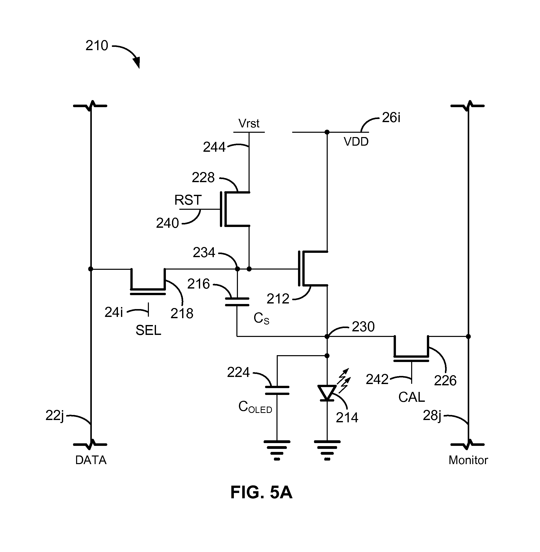
[0064] FIG. 5A is a circuit diagram of an exemplary driving circuit for a pixel 210 that includes a monitor line 28j coupled to the node 230 by a calibration transistor 226 controlled by a CAL line 242, for reading the current values of operating parameters such as the drive current and the OLED voltage. The circuit of FIG. 5A also includes a reset transistor 228 for controlling the application of a reset voltage Vrst to the gate of the drive transistor 212. The drive transistor 212, the switching transistor 218 and the OLED 214 are the same as described above in the circuit of FIG. 2A.
[0065] FIG. 5B is a schematic timing diagram of exemplary operation cycles for the pixel 210 shown in FIG. 5A. At the beginning of the cycle 252, the RST and CAL lines go high at the same time, thereby turning on both the transistors 228 and 226 for the cycle 252, so that a voltage is applied to the monitor line 28j. The drive transistor 212 is on, and the OLED 214 is off. During the next cycle 254, the RST line stays high while the CAL line goes low to turn off the transistor 226, so that the drive transistor 212 charges the node 230 until the drive transistor 212 is turned off, e.g., by the RST line going low at the end of the cycle 254. At this point the gate-source voltage Vgs of the drive transistor 212 is the Vt of that transistor. If desired, the timing can be selected so that the drive transistor 212 does not turn off during the cycle 254, but rather charges the node 230 slightly. This charge voltage is a function of the mobility, Vt and other parameters of the transistor 212 and thus can compensate for all these parameters.
[0066] During the programming cycle 258, the SEL line 24i goes high to turn on the switching transistor 218. This connects the gate of the drive transistor 212 to the DATA line, which charges the the gate of transistor 212 to Vp. The gate-source voltage Vgs of the transistor 212 is then Vp+Vt, and thus the current through that transistor is independent of the threshold voltage Vt:
I = ( Vgs - Vt ) 2 = ( Vp + Vt - Vt ) 2 = Vp 2 ##EQU00001##
[0067] The timing diagrams in FIGS. 5C and 5D as described above for the timing diagram of FIG. 5B, but with symmetric signals for CAL and RST so they can be shared, e.g., CAL[n] can be used as RST[n-1].
[0068] FIG. 5E illustrates a timing diagram that permits the measuring of the OLED voltage and/or current through the monitor line 28j while the RST line is high to turn on the transistor 228, during the cycle 282, while the drive transistor 212 is off.
[0069] FIG. 5F illustrates a timing diagram that offers functionality similar to that of FIG. 5E. However, with the timing shown in FIG. 5F, each pixel in a given row n can use the reset signal from the previous row n-1 (RST[n-1]) as the calibration signal CAL[n] in the current row n, thereby reducing the number of signals required.
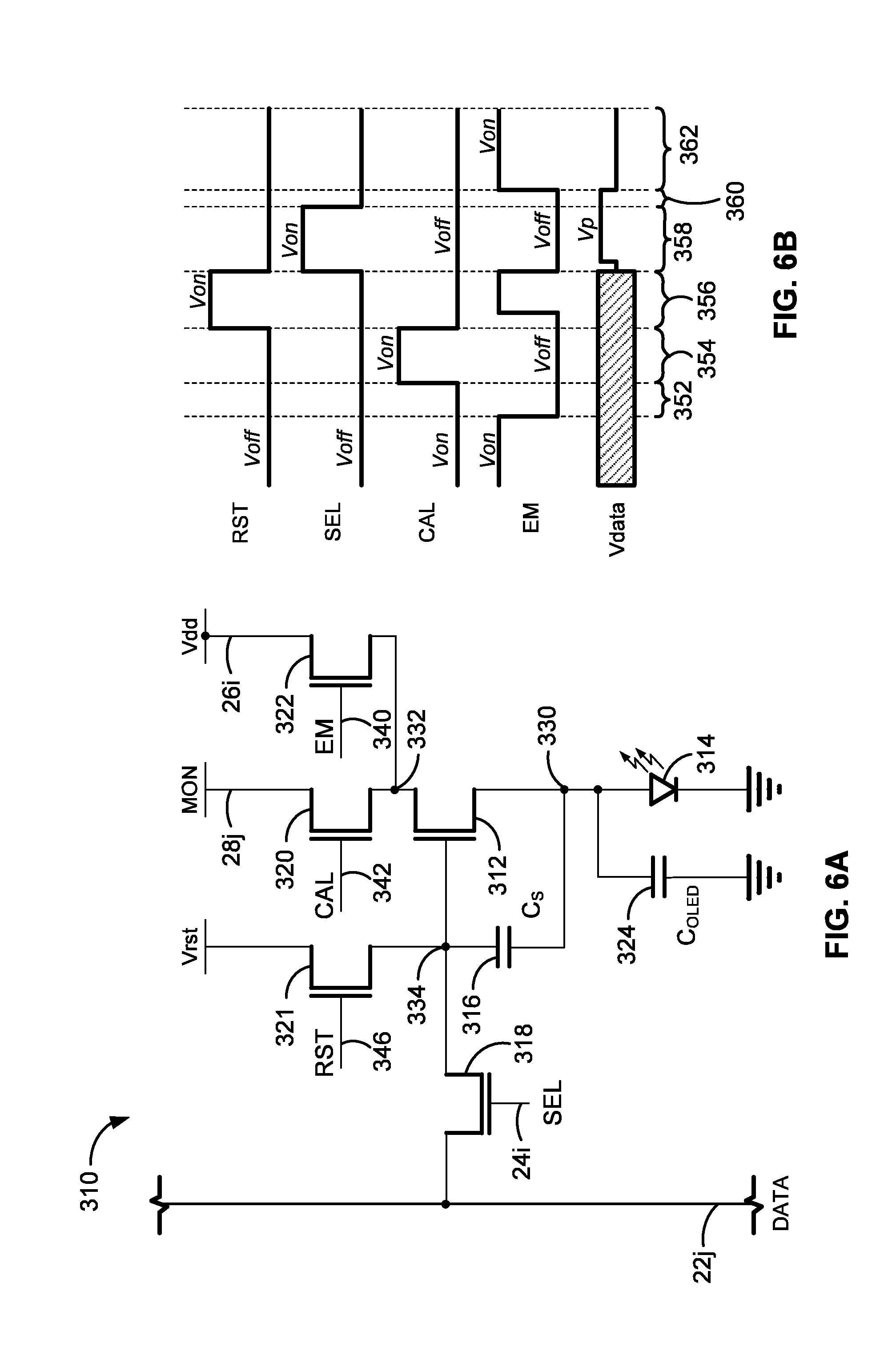
[0070] FIG. 6A is a circuit diagram of an exemplary driving circuit for a pixel 310 that includes a calibration transistor 320 between the drain of the drive transistor 312 and a MON/Vref2 line 28j for controlling the application of a voltage Vref2 to the node 332, which is the drain of the drive transistor 312. The circuit in FIG. 6A also includes an emission transistor 322 between the drain of the drive transistor 312 and a VDD line 26i, for controlling the application of the voltage Vdd to the node 332. The drive transistor 312, the switching transistor 318, the reset transistor 321 and the OLED 214 are the same as described above in the circuit of FIG. 5A.
[0071] FIG. 6B is a schematic timing diagram of exemplary operation cycles for the pixel 310 shown in FIG. 6A. At the beginning of the cycle 352, the EM line goes low to turn off the emission transistor 322 so that the voltage Vdd is not applied to the drain of the drive transistor 312. The emission transistor remains off during the second cycle 354, when the CAL line goes high to turn on the calibration transistor 320, which connects the MON/Vref2 line 28j to the node 332. This charges the node 332 to a voltage that is smaller that the ON voltage of the OLED. At the end of the cycle 354, the CAL line goes low to turn off the calibration transistor 320. Then during the next cycle 356, and the RST and EM successively go high to turn on transistors 321 and 322, respectively, to connect (1) the Vrst line to a node 334, which is the gate terminal of the storage capacitor 316 and (2) the VDD line 26i to the node 332. This turns on the drive transistor 312 to charge the node 330 to a voltage that is a function of Vt and other parameters of the drive transistor 312.
[0072] At the beginning of the next cycle 358 shown in FIG. 6B, the RST and EM lines go low to turn off the transistors 321 and 322, and then the SEL line goes high to turn on the switching transistor 318 to supply a programming voltage Vp to the gate of the drive transistor 312. The node 330 at the source terminal of the drive transistor 312 remains substantially the same because the capacitance C.sub.OLED of the OLED 314 is large. Thus, the gate-source voltage of the transistor 312 is a function of the mobility, Vt and other parameters of the drive transistor 312 and thus can compensate for all these parameters.
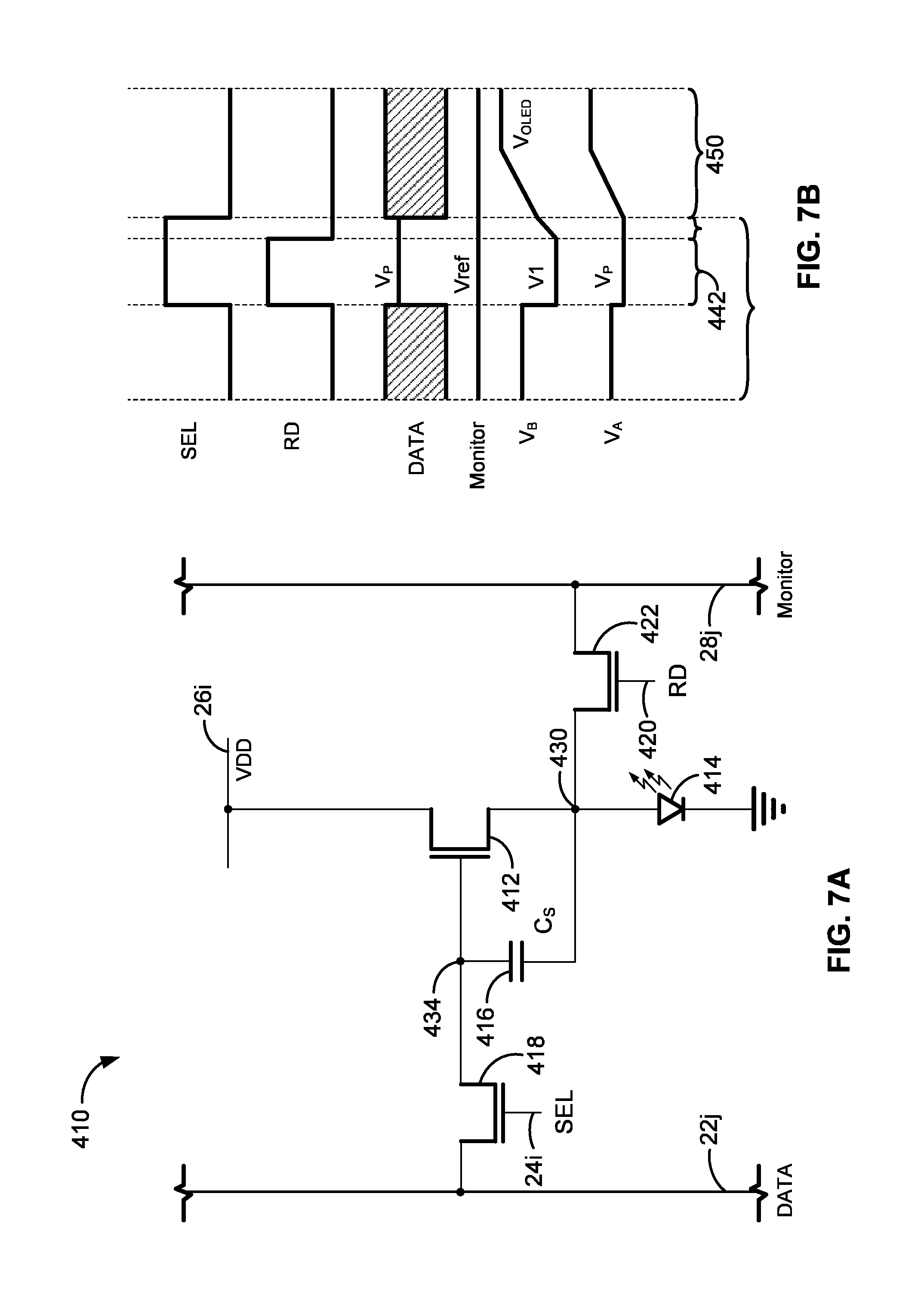
[0073] FIG. 7A is a circuit diagram of another exemplary driving circuit that modifies the gate-source voltage Vgs of the drive transistor 412 of a pixel 410 to compensate for variations in drive transistor parameters due to process variations, aging and/or temperature variations. This circuit includes a monitor line 28j coupled to the node 430 by a read transistor 422 controlled by a RD line 420, for reading the current values of operating parameters such as drive current and Voled. The drive transistor 412, the switching transistor 418 and the OLED 414 are the same as described above in the circuit of FIG. 2A.
[0074] FIG. 7B is a schematic timing diagram of exemplary operation cycles for the pixel 410 shown in FIG. 7A. At the beginning of the first phase 442 of a programming cycle 446, the SEL and RD lines both go high to (1) turn on a switching transistor 418 to charge the gate of the drive transistor 412 to a programming voltage Vp from the data line 22j, and (2) turn on a read transistor 422 to charge the source of the transistor 412 (node 430) to a voltage Vref from a monitor line 28j. During the second phase 444 of the programming cycle 446, the RD line goes low to turn off the read transistor 422 so that the node 430 is charged back through the transistor 412, which remains on because the SEL line remains high. Thus, the gate-source voltage of the transistor 312 is a function of the mobility, Vt and other parameters of the transistor 212 and thus can compensate for all these parameters.
[0075] FIG. 8A is a circuit diagram of an exemplary driving circuit for a pixel 510 which adds an emission transistor 522 to the pixel circuit of FIG. 7A, between the source side of the storage capacitor 522 and the source of the drive transistor 512. The drive transistor 512, the switching transistor 518, the read transistor 520, and the OLED 414 are the same as described above in the circuit of FIG. 7A.
[0076] FIG. 8B is a schematic timing diagram of exemplary operation cycles for the pixel 510 shown in FIG. 8A. As can be seen in FIG. 8B, the EM line is low to turn off the emission transistor 522 during the entire programming cycle 554, to produce a black frame. The emission transistor is also off during the entire measurement cycle controlled by the RD line 540, to avoid unwanted effects from the OLED 514. The pixel 510 can be programmed with no in-pixel compensation, as illustrated in FIG. 8B, or can be programmed in a manner similar to that described above for the circuit of FIG. 2A.
[0077] FIG. 9A is a circuit diagram of an exemplary driving circuit for a pixel 610 which is the same as the circuit of FIG. 8A except that the single emission transistor is replaced with a pair of emission transistors 622a and 622b connected in parallel and controlled by two different EM lines EMa and EMb. The two emission transistors can be used alternately to manage the aging of the emission transistors, as illustrated in the two timing diagrams in FIGS. 9B and 9C. In the timing diagram of FIG. 9B, the EMa line is high and the EMAb line is low during the first phase of a driving cycle 660, and then the EMa line is low and the EMAb line is high during the second phase of that same driving cycle. In the timing diagram of FIG. 9C, the EMa line is high and the EMAb line is low during a first driving cycle 672, and then the EMa line is low and the EMAb line is high during a second driving cycle 676.
[0078] FIG. 10A is a circuit diagram of an exemplary driving circuit for a pixel 710 which is similar to the circuit of FIG. 3A described above, except that the circuit in FIG. 10A adds a monitor line 28j, the EM line controls both the Vref transistor 742 and the emission transistor 722, and the drive transistor 712 and the emission transistor 722 have separate connections to the VDD line. The drive transistor 12, the switching transistor 18, the storage capacitor 716, and the OLED 414 are the same as described above in the circuit of FIG. 3A.
[0079] As can be seen in the timing diagram in FIG. 10B, the EM line 740 goes high and remains high during the programming cycle to turn off the p-type emission transistor 722. This disconnects the source side of the storage capacitor 716 from the VDD line 26i to protect the pixel 710 from fluctuations in the VDD voltage during the programming cycle, thereby avoiding any effect of VDD variations on the pixel current. The high EM line also turns on the n-type reference transistor 742 to connect the source side of the storage capacitor 716 to the Vrst line 744, so the capacitor terminal B is charged to Vrst. The gate voltage of the drive transistor 712 is high, so the drive transistor 712 is off. The voltage on the gate side of the capacitor 716 is controlled by the WR line 745 connected to the gate of the switching transistor 718 and, as shown in the timing diagram, the WR line 745 goes low during a portion of the programming cycle to turn on the p-type transistor 718, thereby applying the programming voltage Vp to the gate of the drive transistor 712 and the gate side of the storage capacitor 716.
[0080] When the EM line 740 goes low at the end of the programming cycle, the transistor 722 turns on to connect the capacitor terminal B to the VDD line. This causes the gate voltage of the drive transistor 712 to go to Vdd-Vp, and the drive transistor turns on. The charge on the capacitor is Vrst-Vdd-Vp. Since the capacitor 716 is connected to the VDD line during the driving cycle, any fluctuations in Vdd will not affect the pixel current.
[0081] FIG. 10C is a timing diagram for a TFT read operation, which takes place during an interval when both the RD and EM lines are low and the WR line is high, so the emission transistor 722 is on and the switching transistor 718 is off. The monitor line 28j is connected to the source of the drive transistor 712 during the interval when the RD line 746 is low to turn on the read transistor 726, which overlaps the interval when current if flowing through the drive transistor to the OLED 714, so that a reading of that current flowing through the drive transistor 712 can be taken via the monitor line 28j.
[0082] FIG. 10D is a timing diagram for an OLED read operation, which takes place during an interval when the RD line 746 is low and both the EM and WR lines are high, so the emission transistor 722 and the switching transistor 718 are both off. The monitor line 28j is connected to the source of the drive transistor 712 during the interval when the RD line is low to turn on the read transistor 726, so that a reading of the voltage on the anode of the OLED 714 can be taken via the monitor line 28j.
[0083] While particular embodiments and applications of the present invention have been illustrated and described, it is to be understood that the invention is not limited to the precise construction and compositions disclosed herein and that various modifications, changes, and variations can be apparent from the foregoing descriptions without departing from the spirit and scope of the invention as defined in the appended claims.
* * * * *
D00000
D00001
D00002
D00003
D00004
D00005
D00006
D00007
D00008
D00009
D00010
D00011
D00012
D00013

D00014

D00015

D00016

D00017

D00018

D00019

D00020


XML
uspto.report is an independent third-party trademark research tool that is not affiliated, endorsed, or sponsored by the United States Patent and Trademark Office (USPTO) or any other governmental organization. The information provided by uspto.report is based on publicly available data at the time of writing and is intended for informational purposes only.
While we strive to provide accurate and up-to-date information, we do not guarantee the accuracy, completeness, reliability, or suitability of the information displayed on this site. The use of this site is at your own risk. Any reliance you place on such information is therefore strictly at your own risk.
All official trademark data, including owner information, should be verified by visiting the official USPTO website at www.uspto.gov. This site is not intended to replace professional legal advice and should not be used as a substitute for consulting with a legal professional who is knowledgeable about trademark law.