Methods For Depositing A Doped Germanium Tin Semiconductor And Related Semiconductor Device Structures
Kohen; David ; et al.
U.S. patent application number 15/683701 was filed with the patent office on 2019-02-28 for methods for depositing a doped germanium tin semiconductor and related semiconductor device structures. The applicant listed for this patent is ASM IP Holding B.V.. Invention is credited to David Kohen, Harald Benjamin Profijt.
| Application Number | 20190067004 15/683701 |
| Document ID | / |
| Family ID | 65435535 |
| Filed Date | 2019-02-28 |
| United States Patent Application | 20190067004 |
| Kind Code | A1 |
| Kohen; David ; et al. | February 28, 2019 |
METHODS FOR DEPOSITING A DOPED GERMANIUM TIN SEMICONDUCTOR AND RELATED SEMICONDUCTOR DEVICE STRUCTURES
Abstract
A method for depositing a germanium tin (Ge.sub.1-xSn.sub.x) semiconductor is disclosed. The method may include; providing a substrate within a reaction chamber, heating the substrate to a deposition temperature and exposing the substrate to a germanium precursor and a tin precursor. The method may further include; depositing a germanium tin (Ge.sub.1-xSn.sub.x) semiconductor on the surface of the substrate, and exposing the germanium tin (Ge.sub.1-xSn.sub.x) semiconductor to a boron dopant precursor. Semiconductor device structures including a germanium tin (Ge.sub.1-xSn.sub.x) semiconductor formed by the methods of the disclosure are also provided.
| Inventors: | Kohen; David; (Phoenix, AZ) ; Profijt; Harald Benjamin; (Veldhoven, NL) | ||||||||||
| Applicant: |
|
||||||||||
|---|---|---|---|---|---|---|---|---|---|---|---|
| Family ID: | 65435535 | ||||||||||
| Appl. No.: | 15/683701 | ||||||||||
| Filed: | August 22, 2017 |
| Current U.S. Class: | 1/1 |
| Current CPC Class: | H01L 29/0653 20130101; H01L 21/02579 20130101; H01L 29/66795 20130101; H01L 21/76895 20130101; H01L 29/7851 20130101; H01L 29/165 20130101; C30B 25/02 20130101; H01L 21/02532 20130101; H01L 29/66803 20130101; H01L 29/0847 20130101; H01L 29/167 20130101; H01L 29/161 20130101; C30B 29/52 20130101; H01L 29/7848 20130101; H01L 29/66636 20130101; H01L 21/28518 20130101; C23C 16/06 20130101; C30B 33/02 20130101; H01L 29/45 20130101; C23C 16/56 20130101; H01L 23/535 20130101; H01L 21/0262 20130101; H01L 21/02535 20130101 |
| International Class: | H01L 21/02 20060101 H01L021/02; H01L 29/66 20060101 H01L029/66; H01L 21/285 20060101 H01L021/285; H01L 21/768 20060101 H01L021/768; H01L 29/165 20060101 H01L029/165; H01L 29/08 20060101 H01L029/08; H01L 29/78 20060101 H01L029/78; H01L 29/06 20060101 H01L029/06; H01L 29/45 20060101 H01L029/45; H01L 23/535 20060101 H01L023/535; C30B 29/52 20060101 C30B029/52; C30B 25/02 20060101 C30B025/02; C23C 16/06 20060101 C23C016/06 |
Claims
1. A method of depositing a doped germanium tin (Ge.sub.1-xSn.sub.x) semiconductor comprising: providing a substrate within a reaction chamber; heating the substrate to a deposition temperature; exposing the substrate to a germanium precursor and a tin precursor in the reaction chamber; depositing a germanium tin (Ge.sub.1-xSn.sub.x) semiconductor on a surface of the substrate; removing the germanium precursor and the tin precursor from the reaction chamber; after the step of depositing, exposing the germanium tin (Ge.sub.1-xSn.sub.x) semiconductor to a boron dopant precursor while no tin precursor and no germanium precursor are introduced to the reaction chamber; and after the step of exposing, annealing the germanium tin (Ge.sub.1-xSn.sub.x) semiconductor.
2. The method of claim 1, further comprising a pre-deposition bake.
3. The method of claim 1, wherein exposing the substrate to the germanium precursor and the tin precursor further comprises exposing the substrate to an initial boron dopant precursor.
4. The method of claim 1, wherein heating the substrate to the deposition temperature further comprises heating the substrate to a deposition temperature of between approximately 275.degree. C. and approximately 400.degree. C.
5. The method of claim 1, further comprising selecting the germanium precursor to comprise at least one of: germane (GeH.sub.4), digermane (Ge.sub.2H.sub.6), trigermane (Ge.sub.3H.sub.8), or germylsilane (GeH.sub.6Si).
6. The method of claim 1, further comprising selecting the tin precursor to comprise at least one of tin tetrachloride (SnCl.sub.4) or tin deuteride (SnD.sub.4).
7. The method of claim 1, further comprising selecting the boron dopant precursor to comprise at least one of diborane (B.sub.2H.sub.6) or boron trichloride (BCl.sub.3).
8. The method of claim 1, wherein exposing the substrate to the germanium precursor and the tin precursor further comprises co-flowing the germanium precursor and the tin precursor into the reaction chamber.
9. The method of claim 1, wherein depositing the germanium tin (Ge.sub.1-xSn.sub.x) semiconductor on the surface of the substrate further comprises depositing the germanium tin (Ge.sub.1-xSn.sub.x) semiconductor to a thickness of between approximately 1 nanometer to approximately 15 nanometers.
10. The method of claim 1, wherein exposing the germanium tin (Ge.sub.1-xSn.sub.x) semiconductor to the boron dopant precursor further comprises exposing the germanium tin (Ge.sub.1-xSn.sub.x) semiconductor to the boron dopant precursor for a time period of between approximately 1 second and approximately 60 seconds.
11. The method of claim 1, wherein a deposition cycle comprises: exposing the substrate to the germanium precursor and the tin precursor, depositing the germanium tin (Ge.sub.1-xSn.sub.x) semiconductor, and exposing the germanium tin (Ge.sub.1-xSn.sub.x) semiconductor to the boron dopant precursor.
12. The method of claim 11, further comprising performing two or more deposition cycles prior to the step of annealing.
13. The method of claim 12, wherein performing two or more deposition cycles further comprises depositing the germanium tin (Ge.sub.1-xSn.sub.x) semiconductor to a thickness of between approximately 40 nanometers and approximately 60 nanometers.
14. The method of claim 1, wherein exposing the germanium tin (Ge.sub.1-xSn.sub.x) semiconductor to the boron dopant precursor further comprises doping the germanium tin (Ge.sub.1-xSn.sub.x) semiconductor to a dopant concentration of greater than 1.times.10.sup.21 dopants per cubic centimeter.
15. The method of claim 12, wherein the step of annealing the germanium tin (Ge.sub.1-xSn.sub.x) semiconductor is performed at a temperature between approximately 350.degree. C. and approximately 650.degree. C. after performing two or more deposition cycles.
16. The method of claim 1, wherein depositing the germanium tin (Ge.sub.1-xSn.sub.x) semiconductor on the surface of the substrate further comprises depositing the germanium tin (Ge.sub.1-xSn.sub.x) with a tin (Sn) content of greater than approximately x=0.05.
17. A semiconductor device structure comprising the germanium tin (Ge.sub.1-xSn.sub.x) semiconductor deposited by the method of claim 1.
18. The semiconductor device structure of claim 17, wherein the germanium tin (Ge.sub.1-xSn.sub.x) semiconductor comprises at least one of a source or a drain region of a transistor structure.
19. The semiconductor device structure of claim 18, wherein the transistor structure comprises a PMOSFET.
20. The semiconductor device structure of claim 18, further comprising forming an electrical contact to the source or drain region of the transistor structure, wherein the electrical contact has an electrical resistivity of less than 1.times.10.sup.-9 Ohmcm.sup.2.
Description
FIELD OF INVENTION
[0001] The present disclosure generally relates to methods for depositing a germanium tin (Ge.sub.1-xSn.sub.x) semiconductor and related device structures containing a germanium tin (Ge.sub.1-xSn.sub.x) semiconductor. The present disclosure also generally relates to methods for doping a germanium tin (Ge.sub.1-xSn.sub.x) semiconductor.
BACKGROUND OF THE DISCLOSURE
[0002] There is a growing interest in tin-containing semiconductor materials like germanium tin (Ge.sub.1-xSn.sub.x) for many applications, such as, high mobility channel and strain engineering for advanced microelectronic devices, direct bandgap Group IV materials for photonic devices, or GeSn alloys for photovoltaic devices.
[0003] Monocrystalline germanium tin (Ge.sub.1-xSn.sub.x) semiconductor materials may be deposited or grown using a variety of techniques. For example, vacuum processes, including molecular beam epitaxy and chemical vapor deposition, may be used to form monocrystalline germanium tin (Ge.sub.1-xSn.sub.x) semiconductors.
[0004] In some semiconductor device applications, the germanium tin (Ge.sub.1-xSn.sub.x) semiconductor may be doped with select impurities to obtain a desired electrical conductivity. For example, the germanium tin (Ge.sub.1-xSn.sub.x) semiconductor may be doped p-type by the incorporation of boron into the germanium tin (Ge.sub.1-xSn.sub.x) semiconductor. However, in some applications it may be desirable to deposit or grow a germanium tin (Ge.sub.1-xSn.sub.x) semiconductor which not only has a high p-type doping concentration but also has a significant tin (Sn) composition. For example, for a germanium tin (Ge.sub.1-xSn.sub.x) semiconductor with a tin (Sn) composition greater than x=0.03, it may be difficult to obtain a doping concentration greater than 1.times.10.sup.20 dopants per cubic centimeter. Hence, there is a tradeoff between the tin (Sn) composition and the doping concentration when depositing or growing germanium tin (Ge.sub.1-xSn.sub.x) semiconductor materials. Accordingly, methods are desired for forming a germanium tin (Ge.sub.1-xSn.sub.x) semiconductor with significant tin (Sn) composition and a high doping concentration.
SUMMARY OF THE DISCLOSURE
[0005] In accordance with at least one embodiment of the disclosure, a method for depositing a doped germanium tin (Ge.sub.1-xSn.sub.x) semiconductor is disclosed. The method may comprise: providing a substrate within a reaction chamber, heating the substrate to a deposition temperature, and exposing the substrate to a germanium precursor and a tin precursor. The method may further comprise: depositing a germanium tin (Ge.sub.1-xSn.sub.x) semiconductor on the surface of the substrate, and exposing the germanium tin (Ge.sub.1-xSn.sub.x) semiconductor to a boron dopant precursor. The embodiments of the disclosure may also include semiconductor device structures which may comprise a doped germanium tin (Ge.sub.1-xSn.sub.x) semiconductor formed by the methods of the disclosure.
[0006] For purposes of summarizing the invention and the advantages achieved over the prior art, certain objects and advantages of the invention have been described herein above. Of course, it is to be understood that not necessarily all such objects or advantages may be achieved in accordance with any particular embodiment of the invention. Thus, for example, those skilled in the art will recognize that the invention may be embodied or carried out in a manner that achieves or optimizes one advantage or group of advantages as taught or suggested herein without necessarily achieving other objects or advantages as may be taught or suggested herein.
[0007] All of these embodiments are intended to be within the scope of the invention herein disclosed. These and other embodiments will become readily apparent to those skilled in the art from the following detailed description of certain embodiments having reference to the attached figures, the invention not being limited to any particular embodiment(s) disclosed.
BRIEF DESCRIPTION OF THE DRAWING FIGURES
[0008] While the specification concludes with claims particularly pointing out and distinctly claiming what are regarded as embodiments of the invention, the advantages of embodiments of the disclosure may be more readily ascertained from the description of certain examples of the embodiments of the disclosure when read in conjunction with the accompanying drawing, in which:
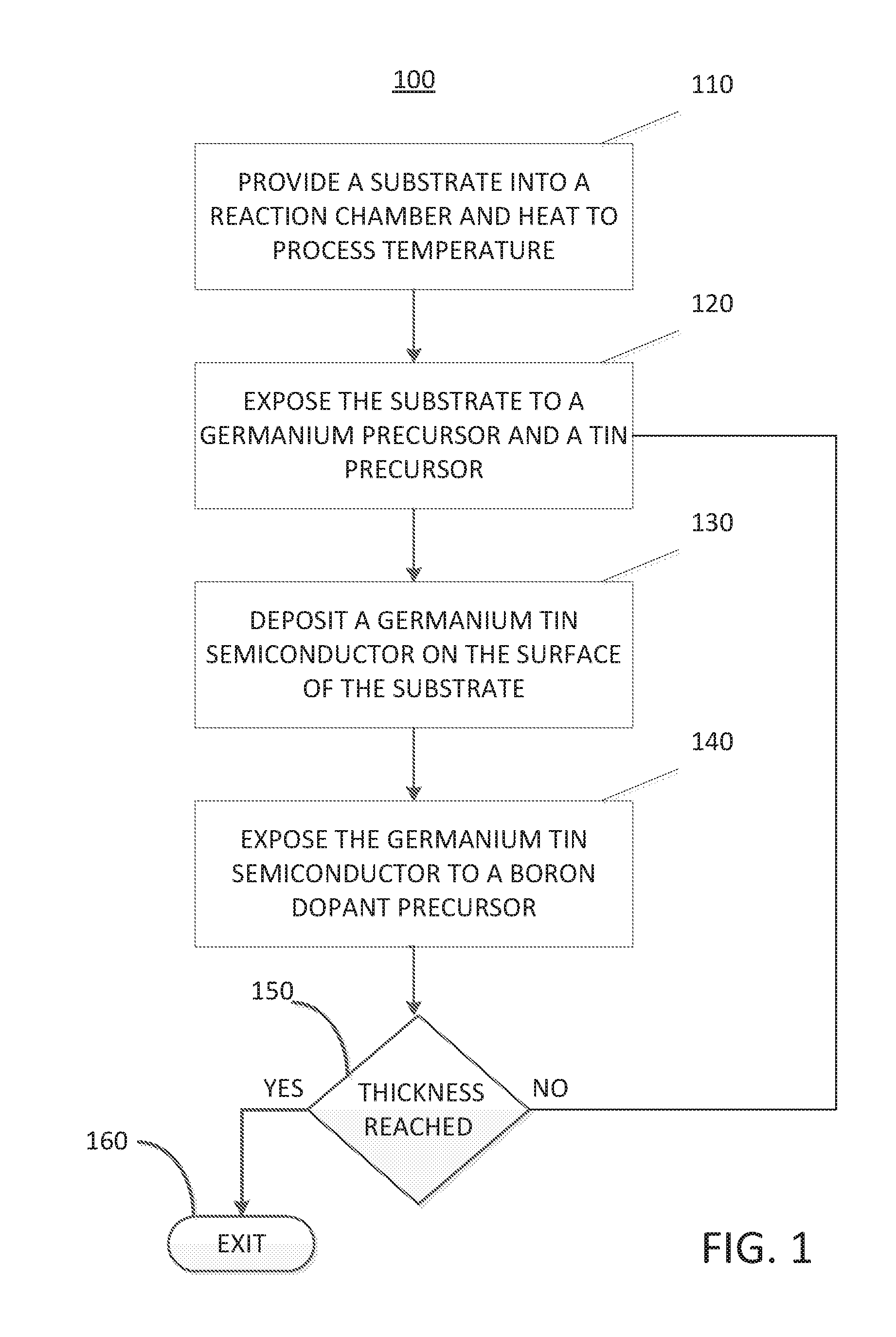
[0009] FIG. 1 illustrates a process flow diagram illustrating an exemplary deposition method in accordance with embodiments of the disclosure;
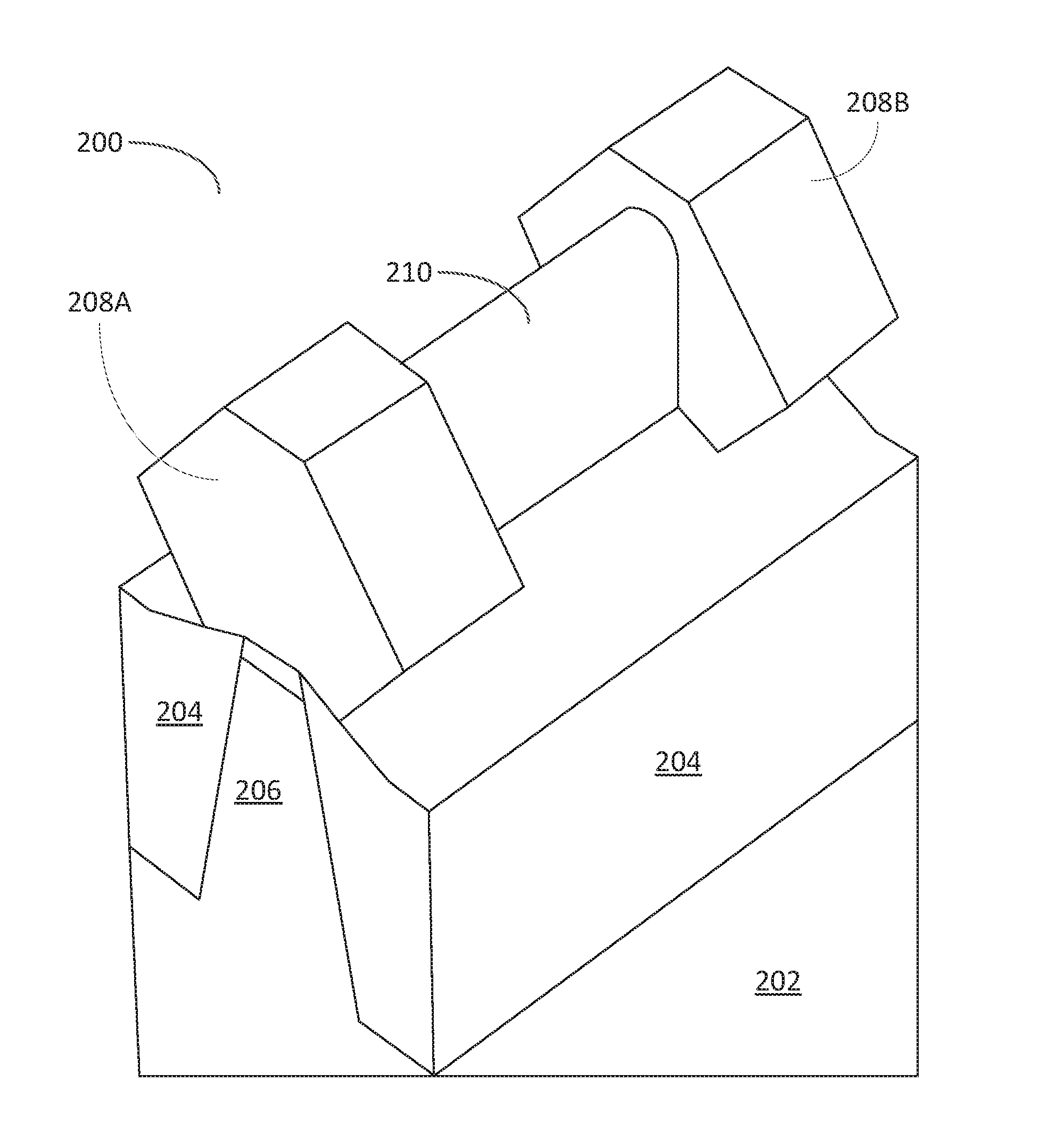
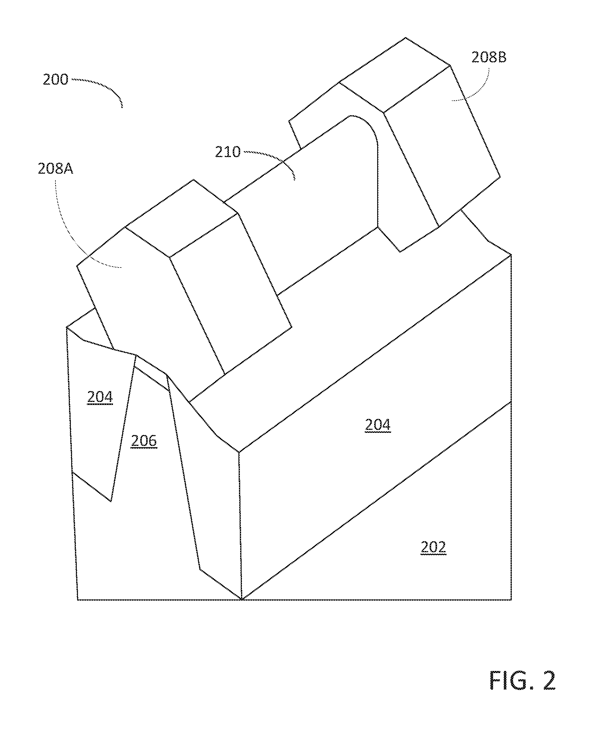
[0010] FIG. 2 illustrates a semiconductor device structure including a germanium tin (Ge.sub.1-xSn.sub.x) semiconductor formed by the embodiments of the disclosure.
[0011] It will be appreciated that elements in the figures are illustrated for simplicity and clarity and have not necessarily been drawn to scale. For example, the dimensions of some of the elements in the figures may be exaggerated relative to other elements to help improve understanding of illustrated embodiments of the present disclosure.
DETAILED DESCRIPTION OF EXEMPLARY EMBODIMENTS
[0012] Although certain embodiments and examples are disclosed below, it will be understood by those in the art that the invention extends beyond the specifically disclosed embodiments and/or uses of the invention and obvious modifications and equivalents thereof. Thus, it is intended that the scope of the invention disclosed should not be limited by the particular disclosed embodiments described below.
[0013] As used herein, the term "substrate" may refer to any underlying material or materials that may be used, or upon which, a device, a circuit or a film may be formed.
[0014] As used herein, the term "epitaxial layer" may refer to a substantially single crystalline layer upon an underlying substantially single crystalline substrate.
[0015] As used herein, the term "chemical vapor deposition" may refer to any process wherein a substrate is exposed to one or more volatile precursors, which react and/or decompose on a substrate surface to produce a desired deposition.
[0016] As used herein, the term "germanium tin" may refer to a semiconductor material comprising germanium and tin and may be represented as Ge.sub.1-xSn.sub.x wherein 1.gtoreq.x.gtoreq.0.
[0017] The embodiments of the disclosure may include methods for forming germanium tin (Ge.sub.1-xSn.sub.x) semiconductor materials and particularly for depositing germanium tin (Ge.sub.1-xSn.sub.x) semiconductors by chemical vapor deposition methods. The embodiments of the disclosure may also include methods for doping the germanium tin semiconductor material with a p-type dopant, wherein the p-type dopant may be provided by a boron dopant precursor, whilst simultaneously incorporating a significant composition of tin (Sn) into the germanium tin (Ge.sub.1-xSn.sub.x) semiconductor material.
[0018] Stress engineering has proven to be critical in achieving improved Si-CMOS device performance at every successive technology node. It is expected that the incorporation of group IV semiconductors and their alloys, and particularly germanium tin (Ge.sub.1-xSn.sub.x) semiconductor materials, may significantly expand the design space for continued bandgap engineering and stress engineering of the silicon (Si)-compatible platform. Germanium tin (Ge.sub.1-zSn.sub.x) semiconductor alloys offer the largest lattice constants of the group IV semiconductors, thereby providing additional flexibility beyond silicon (Si) and silicon germanium (SiGe) for stress engineering germanium (Ge) and silicon germanium (SiGe) based devices. For example, germanium tin (Ge.sub.1-xSn.sub.x) semiconductor materials may not only be utilized for the channel materials for pMOSFET devices, but in addition, the source/drain regions of the pMOSFET device may also comprise germanium tin (Ge.sub.1-xSn.sub.x) semiconductor materials deposited and doped utilizing the embodiments of the disclosure.
[0019] However, to impart significant stress into the semiconductor device structure being fabricated, i.e., a FinFET device, the germanium tin (Ge.sub.1-xSn.sub.x) semiconductor material may require a significant composition of tin (Sn); for example, the composition of the germanium tin (Ge.sub.1-xSn.sub.x) semiconductor material in the source/drain regions may be greater than x=0.08. Conversely, the source/drain regions of the transistor structure may be required to be highly doped, such that the electrical contact resistance to the source/drain regions is kept to a minimum, thereby improving the efficiency of the device. Accordingly, methods and device structures are required, which comprise germanium tin (Ge.sub.1-xSn.sub.x) semiconductor materials which are highly doped (to provide low contact resistance) and comprise a significant tin (Sn) composition (to provide stress to the device structure).
[0020] The methods of the disclosure may be understood with reference to FIG. 1 which illustrates a non-limiting example embodiment of a method for forming a germanium tin (Ge.sub.1-xSn.sub.x) semiconductor material. For example, FIG. 1 may illustrate a method 100 for forming a germanium tin (Ge.sub.1-xSn.sub.x) semiconductor material, which may comprise process block 110 wherein a substrate may be provided into a reaction chamber and the substrate may be heated to process temperature within the reaction chamber. As a non-limiting example, the reaction chamber may comprise a reaction chamber of a chemical vapor deposition system. Embodiments of the present disclosure may be performed in a chemical vapor deposition system available from ASM International N.V. under the name Intrepid.TM. XP or Epsilon.RTM.. However, it is also contemplated that other reaction chambers and alternative chemical vapor deposition system from other manufacturers may also be utilized to perform the embodiments of the present disclosure.
[0021] In some embodiments of the disclosure, the substrate may comprise a planar substrate or a patterned substrate. Patterned substrates may comprise substrates that may include semiconductor device structures formed into or onto a surface of the substrate. For example, the patterned substrates may comprise partially fabricated semiconductor device structures such as transistors and memory elements. The substrate may contain monocrystalline surfaces and/or one or more secondary surfaces that may comprise a non-monocrystalline surface, such as a polycrystalline surface and an amorphous surface. Monocrystalline surfaces may comprise, for example, one or more of silicon (Si), silicon germanium (SiGe), germanium tin (GeSn), or germanium (Ge). Polycrystalline or amorphous surfaces may include dielectric materials, such as oxides, oxynitrides, or nitrides.
[0022] In some embodiments of the disclosure, the substrate may comprise a "virtual substrate," in which a virtual substrate may comprise two or more materials disposed upon one another. For example, a germanium virtual substrate may comprise an upper most exposed germanium growth surface, wherein the virtual substrate may comprise a layer of germanium deposited on another material, e.g., a silicon substrate.
[0023] With continued reference to FIG. 1, the method 100 may continue by heating the substrate to a desired process temperature within a reaction chamber. In some embodiments of the disclosure, the method 100 may comprise heating the substrate to a temperature of less than approximately 400.degree. C., or to a temperature of less than approximately 350.degree. C., or to a temperature of less than approximately 300.degree. C., or even to a temperature of less than approximately 250.degree. C. In some embodiments of the disclosure, the method may comprise heating the substrate to a temperature of between approximately 275.degree. C. and approximately 400.degree. C. In some embodiments of the disclosure, an optional pre-deposition bake may be performed on the substrate after loading the substrate into the reaction chamber and prior to heating the substrate to the process temperature, for example, the substrate may undergo a pre-deposition bake at a temperature between approximately 350.degree. C. and approximately 500.degree. C.
[0024] Once the substrate is heated to the desired process temperature, the method 100 may continue by exposing the substrate to a germanium precursor and a tin precursor, as illustrated by process block 120 of FIG. 1. In some embodiments of the disclosure, both the germanium precursor and the tin precursor may be introduced into the reaction chamber simultaneously, in what is commonly referred to as a "co-flow" process. For example, in some embodiments, the flow rate of the germanium precursor into the reaction chamber may be greater than 50 sccm, or greater than 100 sccm, or even greater than 200 sccm. In addition, in some embodiments, the flow rate of the tin precursor into the reaction chamber may be greater than 0.1 mg/min, or greater than 1 mg/min, or even greater than 5 mg/min.
[0025] In some embodiments of the disclosure, exposing the substrate to a germanium precursor may further comprise selecting the germanium precursor to comprise at least one of germane (GeH.sub.4), digermane (Ge.sub.2H.sub.6), trigermane (Ge.sub.3H.sub.8), or germylsilane (GeH.sub.6Si). In some embodiments of the disclosure, the germanium precursor may comprise a Si--Ge-hydride precursor such as (H.sub.3Ge).sub.xSiH.sub.4-x, where x=1-4, or (H.sub.3Si).sub.XGeH.sub.4-x, where x=1-4. In some embodiments of the disclosure, it may be advantageous to further incorporate silicon into the deposition process, for example, the flow of precursor may also include silicon precursors such as, but not limited to, silane (SiH.sub.4), disilane (Si.sub.2H.sub.6), trisilane (Si.sub.3H.sub.8), or higher order silane compounds In some embodiments of the disclosure, exposing the substrate to a tin precursor may further comprise selecting the tin precursor to comprise at least one of tin tetrachloride (SnCl.sub.4), or tin deuteride (SnD.sub.4).
[0026] It should be appreciated that whilst the substrate is heated to the deposition temperature and the germanium precursor and the tin precursor are introduced simultaneously into the reaction chamber, the reaction chamber may be maintained at atmospheric pressure or alternatively at a reduced pressure. For example, in some embodiments, the pressure with the reaction chamber may be less than 760 Torr, or even less than 100 Torr, or even less than 10 Torr.
[0027] In some alternative embodiments of the disclosure, exposing the substrate to the germanium precursor and the tin precursor may further comprise exposing the substrate to an initial boron dopant precursor. For example, the germanium precursor, the tin precursor and the initial boron dopant precursor may be simultaneously introduced into the reaction chamber, i.e., in a "co-flow" process. In some embodiments of the disclosure the initial boron dopant precursor may comprise at least one of diborane (B.sub.2H.sub.6), or boron trichloride (BCl.sub.3). The initial boron dopant precursor may be introduced into the reaction chamber at flow rate of greater than 0.01 sccm, or greater than 0.1 sccm, or even greater than 1 sccm.
[0028] The method 100 may continue with process block 130, wherein the method comprises depositing a germanium tin (Ge.sub.1-xSn.sub.x) semiconductor material on the surface of the substrate. In some embodiments of the disclosure, the germanium tin (Ge.sub.1-xSn.sub.x) semiconductor material may comprise a composition of tin (Sn) where x is greater than 0.01, or greater than 0.05, or even greater than 0.08. In some embodiments, depositing the germanium tin (Ge.sub.1-xSn.sub.x) semiconductor material on the surface of the substrate further comprises depositing the germanium tin (Ge.sub.1-xSn.sub.x) semiconductor material to a thickness of between approximately 1 nanometer to approximately 50 nanometers.
[0029] In embodiments wherein the initial boron dopant precursor is not utilized, i.e., the initial boron dopant is not introduced into the reaction chamber during process block 120, the germanium tin (Ge.sub.1-xSn.sub.x) semiconductor material may be initially deposited as an undoped material. It should be noted herein that the term "undoped" may also refer to "unintentionally doped" as the as-deposited germanium tin (Ge.sub.1-xSn.sub.x) semiconductor may comprise impurities and/or defects which may result in unintentional doping of the germanium tin semiconductor. In embodiments wherein the initial boron dopant precursor is utilized, i.e., the initial boron dopant is introduced into the reaction chamber during process block 120, the germanium tin (Ge.sub.1-xSn.sub.x) semiconductor may be initially deposited as a p-type germanium tin semiconductor with an initial carrier concentration of greater than 1.times.10.sup.18 dopants per cubic centimeter, or greater than 1.times.10.sup.19 dopants per cubic centimeter, or even greater than 1.times.10.sup.20 dopants per cubic centimeter.
[0030] The method 100 of depositing a p-type doped germanium tin (Ge.sub.1-xSn.sub.x) semiconductor material may continue after process block 130, i.e., after depositing the germanium tin semiconductor on the surface of the substrate, by ceasing the flow of all the precursor gases into the reaction chamber. For example, in some embodiments, the method may further comprise removing the germanium precursor and the tin precursor from the reaction chamber after depositing the germanium tin (Ge.sub.1-xSn.sub.x) semiconductor on the surface of the substrate. In addition to ceasing the flow of the germanium precursor and the tin precursor, the germanium precursor and tin precursor that remains in the reaction chamber, after deposition of the germanium tin, may be evacuated from the reaction chamber by the vacuum system fluidly connected to the reaction chamber.
[0031] The method 100 may continue with process block 140, which comprises exposing the deposited germanium tin (Ge.sub.1-xSn.sub.x) semiconductor material to a boron dopant precursor. For example, in some embodiments the method may comprise selecting the boron dopant precursor to comprise at least one of diborane (B.sub.2H.sub.6), or boron trichloride (BCl.sub.3). In addition, in some embodiments the boron dopant precursor may be introduced into the reaction chamber with a flow rate greater than 0.01 sccm, or greater than 0.1 sccm, or even greater than 1 sccm. In some embodiments of the disclosure, exposing the germanium tin (Ge.sub.1-xSn.sub.x) semiconductor material to the boron dopant precursor may further comprise exposing the germanium tin (Ge.sub.1-xSn.sub.x) semiconductor material to the boron dopant precursor for a time period of between approximately 1 second and approximately 60 seconds. It should be noted that during the germanium tin (Ge.sub.1-xSn.sub.x) semiconductor material exposure to the boron dopant precursor, no germanium precursor or tin precursor is introduced into the reaction chamber, i.e., the boron dopant precursor is separately and solely introduced into the reaction chamber.
[0032] The method 100 may proceed with process block 150, wherein a decision gate determines if the method 100 continues or exits. The decision gate of process block 150 is determined based on the thickness of the germanium tin (Ge.sub.1-xSn.sub.x) semiconductor material deposited, for example, if the thickness of the germanium tin semiconductor is insufficient for the desired device structure then the method 100 may return to process block 120 and the processes of exposing the substrate to a germanium precursor and a tin precursor, depositing a germanium tin semiconductor over the surface of the substrate, and exposing the germanium tin semiconductor to a boron dopant precursor may be repeated two or more times. In other words, the method 100 may comprise a deposition cycle, wherein a deposition cycle comprises: exposing the substrate to the germanium precursor and the tin precursor, depositing the germanium tin (Ge.sub.1-xSn.sub.x) semiconductor material, and exposing the germanium tin (Ge.sub.1-xSn.sub.x) semiconductor material to the boron dopant precursor. In some embodiments of the disclosure, the method 100 may comprise performing two or more deposition cycles until a desired thickness of p-type doped germanium tin (Ge.sub.1-xSn.sub.x) semiconductor material is deposited.
[0033] In some embodiments of the disclosure, performing two or more deposition cycles further comprises depositing a germanium tin (Ge.sub.1-xSn.sub.x) semiconductor material to a thickness of between approximately 40 nanometers and approximately 60 nanometers. In addition, performing two or more deposition cycles may comprise depositing a p-type germanium tin (Ge.sub.1-xSn.sub.x) semiconductor material to a desired thickness with a desired dopant concentration. Therefore, method of the disclosure may comprise exposing the germanium tin (Ge.sub.1-xSn.sub.x) semiconductor material to the boron dopant precursor and may further comprise doping the germanium tin (Ge.sub.1-xSn.sub.x) semiconductor material to a dopant concentration of greater than approximately 1.times.10.sup.20 dopants per cubic centimeter, or greater than approximately 5.times.10.sup.20 dopants per cubic centimeter, or even greater than approximately 1.times.10.sup.21 dopants per cubic centimeter. It should be appreciated that the methods of the disclosure enable the deposition of germanium tin (Ge.sub.1-xSn.sub.x) semiconductor materials with significant tin (Sn) composition whilst maintaining a high doping concentration. Therefore, in some embodiments of the disclosure, the methods may comprise depositing a germanium tin (Ge.sub.1-xSn.sub.x) semiconductor material with a tin (Sn) composition greater than x=0.01 with a dopant concentration greater than 1.times.10.sup.21 dopants per cubic centimeter. In other embodiments of the disclosure, the methods may comprise depositing a germanium tin (Ge.sub.1-xSn.sub.x) semiconductor material with a tin (Sn) composition greater than x=0.04 with a dopant concentration greater than 1.times.10.sup.20 dopants per cubic centimeter.
[0034] Once the germanium tin (Ge.sub.1-xSn.sub.x) semiconductor material has been deposited to the desired thickness, composition and dopant concentration, the process may exit 160 and the substrate may be removed from the reaction chamber for additional device fabrication processes. However, in some embodiments of the disclosure, prior to removing the substrate from the reaction chamber, the substrate may be subjected to a post-growth annealing process to possibly further activate the p-type dopants and/or redistribute the p-type dopants throughout the thickness of the germanium tin (Ge.sub.1-xSn.sub.x) semiconductor material. In some embodiments, the post growth anneal of the germanium tin (Ge.sub.1-xSn.sub.x) semiconductor material may be performed after completion of two or more deposition cycles and may further comprise heating the substrate to a temperature between approximately 350.degree. C. and approximately 650.degree. C. In alternative embodiments, the annealing process may performed during each individual deposition cycle after the germanium tin (Ge.sub.1-xSn.sub.x) semiconductor material has been exposed to the boron dopant precursor.
[0035] In some embodiments, the germanium tin (Ge.sub.1-xSn.sub.x) semiconductor material comprising germanium and tin may comprise less than about 20 at-%, less than about 10 at-%, less than about 7 at-%, less than about 5 at-%, less than about 3 at-%, less than about 2 at-%, or less than about 1 at of impurities, that is, elements other than Ge or Sn. In some embodiments, the germanium tin layer comprising germanium and tin comprise less than about 20 at-%, less than about 10 at-%, less than about 5 at-%, less than about 2 at-%, or less than about 1 at-% of hydrogen. In some embodiments, the germanium tin layer comprising germanium and tin may comprise less than about 10 at-%, less than about 5 at-%, less than about 2 at-%, less than about 1 at-% or less than about 0.5 at-% of carbon. In some embodiments, the germanium tin layer comprising germanium and tin may comprise less than about 5 at-%, less than about 2 at-%, less than about 1 at-%, less than about 0.5 at-%, or less than about 0.2 at-% of nitrogen. In some embodiments, the germanium tin layer may comprise less than about 15 at-%, less than about 10 at-%, less than about 5 at-%, less than about 3 at-%, less than about 2 at-%, or less than about 1 at-% of oxygen. In some embodiments, the germanium tin layer may comprise less than about 30 at-%, less than about 20 at-%, less than about 10 at-%, less than about 5 at-%, or less than about 3 at-% of oxygen on average at the surface, wherein the surface can be understood to be thickness of less than about 20 nm from the top most surface. In some embodiments, the thin film comprising germanium and tin may comprise more than about 80 at-%, more than about 90 at-%, more than about 93 at-%, more than about 95 at-%, more than about 97 at-%, or more than about 99 at-% germanium and tin.
[0036] The embodiments of the disclosure may also provide semiconductor device structures comprising germanium tin (Ge.sub.1-xSn.sub.x) semiconductor material deposited by the methods described herein. For example, FIG. 2 illustrates a non-limiting example of a semiconductor device structure 200, wherein the semiconductor device structure 200 comprises a partially fabricated double gate MOSFET, commonly referred to as a FinFET. The semiconductor device structure 200 may comprise a substrate 202, which may comprise a bulk silicon (Si) substrate or alternatively may comprise a "virtual substrate" comprising a germanium virtual substrate with a Si--Ge--Sn alloy grown thereon. The substrate 202 may be doped either with p-type dopants (for NMOS type FinFET devices) or with n-type dopants (for PMOS type FinFET devices). In the non-limiting example semiconductor device structure of FIG. 2, the substrate 202 may comprise n-type dopants and the semiconductor device structure 200 may comprise a PMOSFET or particularly a PMOS FinFET.
[0037] The semiconductor device structure 200 may also comprise isolation regions 204, which may comprise shallow trench isolation (STI) regions. The semiconductor device structure 200 may also comprise a Fin structure 206 disposed between the two isolation regions 204. The semiconductor device structure 200 may comprise epitaxially regrown source and drain regions 208A and 208B which may be deposited utilizing the methods of the disclosure. For example, the source and drain regions 208A and 208B may comprise germanium tin (Ge.sub.1-xSn.sub.x) semiconductor material with a tin (Sn) composition of x=0.08 and a boron doping concentration of greater than approximately 1.times.10.sup.19 dopants per cubic centimeter. The semiconductor device structure 200 may also comprise a channel region 210 formed by the embodiments of the current disclosure. For example, the channel region 210 may comprise a germanium tin (Ge.sub.1-xSn.sub.x) semiconductor material with a tin (Sn) composition of x=0.04 and a boron doping concentration of greater than approximately 1.times.10.sup.18 dopants per cubic centimeter.
[0038] In some embodiments of the disclosure, an electrical contact may be made to the p-type germanium tin (Ge.sub.1-xSn.sub.x) semiconductor material comprising source and drain regions 208A and 208B. In some embodiments, the electrical contact (not shown) may comprise a silicide, such as, for example, a titanium silicide (TiSi.sub.2). The embodiments of the disclosure allow for a high concentration of active p-type carriers in the source and drain regions 208A and 208B which in turn may result in a reduction in the electrical contact resistance to the source and drain regions. For example, the methods of the disclosure may comprise forming an electrical contact to the p-type source and drain regions 208A and 208B, wherein the electrical contact has an electrical resistivity of less than 1.times.10.sup.-8 Ohmcm.sup.2, or less than 5.times.10.sup.-9 Ohmcm.sup.2, or even less than 1.times.10.sup.-9 Ohmcm.sup.2.
[0039] The example embodiments of the disclosure described above do not limit the scope of the invention, since these embodiments are merely examples of the embodiments of the invention, which is defined by the appended claims and their legal equivalents. Any equivalent embodiments are intended to be within the scope of this invention. Indeed, various modifications of the disclosure, in addition to those shown and described herein, such as alternative useful combination of the elements described, may become apparent to those skilled in the art from the description. Such modifications and embodiments are also intended to fall within the scope of the appended claims.
* * * * *
D00000
D00001
D00002
XML
uspto.report is an independent third-party trademark research tool that is not affiliated, endorsed, or sponsored by the United States Patent and Trademark Office (USPTO) or any other governmental organization. The information provided by uspto.report is based on publicly available data at the time of writing and is intended for informational purposes only.
While we strive to provide accurate and up-to-date information, we do not guarantee the accuracy, completeness, reliability, or suitability of the information displayed on this site. The use of this site is at your own risk. Any reliance you place on such information is therefore strictly at your own risk.
All official trademark data, including owner information, should be verified by visiting the official USPTO website at www.uspto.gov. This site is not intended to replace professional legal advice and should not be used as a substitute for consulting with a legal professional who is knowledgeable about trademark law.