Layer Forming Method And Apparatus
Klaver; Arjen ; et al.
U.S. patent application number 15/690017 was filed with the patent office on 2019-02-28 for layer forming method and apparatus. The applicant listed for this patent is ASM IP Holding B.V.. Invention is credited to Lucian Jdira, Arjen Klaver, Werner Knaepen, Ruslan Kvetny, Gido van der Star.
| Application Number | 20190066997 15/690017 |
| Document ID | / |
| Family ID | 65433909 |
| Filed Date | 2019-02-28 |
| United States Patent Application | 20190066997 |
| Kind Code | A1 |
| Klaver; Arjen ; et al. | February 28, 2019 |
LAYER FORMING METHOD AND APPARATUS
Abstract
There is provided a method and apparatus for forming a layer, by sequentially repeating a layer deposition cycle to process a substrate disposed in a reaction chamber. The deposition cycle comprising: supplying a first precursor into the reaction chamber for a first pulse period; supplying a second precursor into the reaction chamber for a second pulse period. At least one of the first and second precursors may be supplied into the reaction chamber for a pretreatment period longer than the first or second pulse period before sequentially repeating the deposition cycles.
| Inventors: | Klaver; Arjen; (Neerijse, BE) ; Knaepen; Werner; (Leuven, BE) ; Jdira; Lucian; (Nieuw Vennep, NL) ; van der Star; Gido; (Leuven, BE) ; Kvetny; Ruslan; (Portland, OR) | ||||||||||
| Applicant: |
|
||||||||||
|---|---|---|---|---|---|---|---|---|---|---|---|
| Family ID: | 65433909 | ||||||||||
| Appl. No.: | 15/690017 | ||||||||||
| Filed: | August 29, 2017 |
| Current U.S. Class: | 1/1 |
| Current CPC Class: | H01L 21/02208 20130101; H01L 21/0228 20130101; C23C 16/345 20130101; C23C 16/4408 20130101; C23C 16/45544 20130101; C23C 16/45527 20130101; C23C 16/52 20130101; H01L 21/02211 20130101; H01L 21/0217 20130101; C23C 16/45553 20130101 |
| International Class: | H01L 21/02 20060101 H01L021/02; C23C 16/52 20060101 C23C016/52; C23C 16/44 20060101 C23C016/44; C23C 16/455 20060101 C23C016/455 |
Claims
1. A method of forming a layer, comprising: providing a substrate in a reaction chamber; sequentially repeating a deposition cycle to deposit at least a portion of the layer on the substrate disposed in the reaction chamber, the deposition cycle comprising: supplying a first precursor into the reaction chamber for a first pulse period; removing a portion of the first precursor from the reaction chamber; supplying a second precursor into the reaction chamber for a second pulse period, and removing a portion of the second precursor from the reaction chamber; wherein at least one of the first and second precursors is supplied into the reaction chamber for a pretreatment period longer than the first or second pulse period before sequentially repeating the deposition cycles.
2. The method according to claim 1, wherein the pretreatment period is between 2 to 1200 times longer than the first or second pulse period.
3. The method according to claim 1, wherein the pretreatment period is between 1 to 60 minutes.
4. The method according to claim 1, wherein sequentially repeating the deposition cycle takes between 1 to 180 minutes.
5. The method according to claim 1, wherein the first pulse period is between 1 to 180 seconds.
6. The method according to claim 1, wherein the second pulse period is between 1 to 180 seconds.
7. The method according to claim 1, wherein the pressure in the reaction chamber is between 0.1 and 1000 Pa.
8. The method according to claim 1, wherein the temperature is between 300 and 900.degree. C.
9. The method according to claim 1, wherein the first precursor comprises a silicon halide.
10. The method according to claim 1, wherein the second precursor comprises a nitriding or oxidizing gas.
11. The method according to claim 1, wherein the first or second precursor is not activated by a plasma.
12. The method according to claim 1, wherein the first precursor is supplied to the reaction chamber between 1 and 20 times longer than the second precursor during sequentially repeating a deposition cycle.
13. The method according to claim 1, wherein both the first and second precursor is supplied into the reaction chamber simultaneously during at least a portion of the pretreatment period.
14. The method according to claim 1, wherein the first precursor from the reaction chamber is removed for a first removal period and the second precursor from the reaction chamber is removed for a second removal period during the deposition cycle, wherein the first and/or second removal period is between 1 to 120 seconds.
15. The method according to claim 13, wherein a purge gas is provided during the first and/or second removal period.
16. The method according to claim 1, wherein the amount of the second precursor supplied to the reaction chamber is between 1 and 25 times more than the first precursor supplied to the reaction chamber during sequentially repeating a deposition cycle.
17. The method according to claim 1, wherein the first and second precursor react with each other to form the layer on the substrate with an atomic layer deposition process.
18. The method according to claim 1, wherein the deposition cycles are repeated between 2 to 100 times.
19. The method according to claim 1, wherein the layer comprises silicon nitride and the silicon concentration in the deposited layer is between 1 to 33% higher than stoichiometric concentration of silicon in Si.sub.3N.sub.4.
20. The method according to claim 1, wherein the method comprises providing a dopant.
21. The method according to claim 1, wherein the method is used in a vertical furnace.
22. A deposition apparatus comprising: a reaction chamber constructed and arranged to hold at least a first substrate; a gas distribution and removal system to provide to and remove from the reaction chamber a first or second precursor; and, a sequence controller operably connected to the gas distribution and removal system and comprising a memory provided with a program to execute deposition of a material on the substrate with the gas distribution and removal system by: sequentially repeating a deposition cycle to deposit at least a portion of the layer on the substrate disposed in the reaction chamber, the cycle comprising: supplying a first precursor into the reaction chamber for a first pulse period; removing a portion of the first precursor from the reaction chamber; supplying a second precursor into the reaction chamber for a second pulse period, and removing a portion of the second precursor from the reaction chamber; wherein the program in the memory is further programmed to control the gas distribution and removal system to supply at least one of the first and second precursors into the reaction chamber for a pretreatment period longer than the first or second pulse period before sequentially repeating the deposition cycles.
Description
FIELD
[0001] The present disclosure generally relates to a method and an apparatus to form a layer on a substrate. More particularly, the disclosure relates to sequentially repeating a deposition cycle to form at least a part of the layer on the substrate for the manufacturing of a semiconductor device.
BACKGROUND
[0002] A substrate placed in a reaction space may be subjected to alternating pulses of at least two different precursors suitable for producing a desired thin layer on the substrate. When the substrate is exposed to a pulse of the first precursor, a layer of the first precursor or reaction products of the first precursor may be formed on the surface of the substrate. For example, a silicon halide molecule may chemisorb on a surface site that has a hydroxyl group. The silicon halide may be H.sub.2SiCl.sub.2 which may chemisorb as a H.sub.2SiCl reaction product, with HCl released as a gaseous byproduct.
[0003] The excess of the first precursor may then be removed from the surface, for example by purging the reaction space with an inert gas and/or evacuating the reaction space. Subsequently, the substrate may be exposed to a pulse of a second precursor reactant, which chemically reacts with the adsorbed portion of the first precursor reactant molecules. Fragments of the second precursor reactant will be adsorbed under some reaction conditions.
[0004] For example, when ammonia (NH.sub.3) is used as the second precursor reactant it may leave fragments such as N, NH or NH.sub.2 groups in the layer. Reaction conditions such as temperature and pressure may be chosen to ensure that a required layer of the first or second precursor may be created. In this way the growth of the film proceeds layer by layer.
[0005] It has been found that there may be a need to improve the quality of the deposited layers.
SUMMARY
[0006] Accordingly in an embodiment, there is provided a method of forming a layer, comprising:
[0007] providing a substrate in a reaction chamber;
[0008] sequentially repeating a deposition cycle to deposit at least a portion of the layer on the substrate disposed in the reaction chamber, the deposition cycle comprising:
[0009] supplying a first precursor into the reaction chamber for a first pulse period;
[0010] removing a portion of the first precursor from the reaction chamber;
[0011] supplying a second precursor into the reaction chamber for a second pulse period, and
[0012] removing a portion of the second precursor from the reaction chamber. At least one of the first and second precursors may be supplied into the reaction chamber for a pretreatment period longer than the first or second pulse period before sequentially repeating the deposition cycles.
[0013] At least one of the first and second precursor may react into byproducts in the reaction chamber during the pretreatment period. By supplying at least one of the first and second precursor in the reaction chamber for the pretreatment period longer than the first or second cycle period, the byproduct may be more uniformly spread through the reaction chamber. Since byproducts may play an important role in preparing the bare surface for deposition of the first, nucleation layer, the uniformity of the nucleation layer may be improved when the byproduct may be better spread through the reaction chamber during the pretreatment period. The uniformity of the first, nucleation layer may have a large influence on the quality of the deposited layer afterwards since subsequent layers may be more easily deposited on the nucleation layer.
[0014] It may be that, during the pretreatment period, the surface may be prepared uniformly for the nucleation layer, but that no actual nucleation layer is deposited. It may also be that, during the pretreatment period, a thin nucleation layer may be deposited.
[0015] According to an embodiment there is provided a deposition apparatus comprising:
[0016] a reaction chamber constructed and arranged to hold at least a first substrate;
[0017] a gas distribution and removal system to provide to and remove from the reaction chamber a first or second precursor; and,
[0018] a sequence controller operably connected to the gas distribution and removal system and comprising a memory provided with a program to execute deposition of a material on the substrate with the gas distribution and removal system by:
[0019] sequentially repeating a deposition cycle to deposit at least a portion of the layer on the substrate disposed in the reaction chamber, the cycle comprising: [0020] supplying a first precursor into the reaction chamber for a first pulse period; [0021] removing a portion of the first precursor from the reaction chamber; [0022] supplying a second precursor into the reaction chamber for a second pulse period, and [0023] removing a portion of the second precursor from the reaction chamber;
[0024] wherein the program in the memory is further programmed to control the gas distribution and removal system to supply at least one of the first and second precursors into the reaction chamber for a pretreatment period longer than the first or second pulse period before sequentially repeating the deposition cycles.
[0025] In some other embodiments, a method for semiconductor processing may be provided. The method includes depositing a silicon film on a substrate.
BRIEF DESCRIPTION OF THE DRAWINGS
[0026] FIG. 1 shows a flowchart illustrating a method of depositing a layer according to an embodiment.
DETAILED DESCRIPTION
[0027] A silicon nitride (SIN) layer may be used as an insulating film in a semiconductor device. The SiN layer may be deposited in a vertical furnace apparatus of the batch type by chemical vapor deposition (CVD) on a plurality of semiconductor wafers. During deposition, alternately, a Si source gas and a nitriding gas may be supplied to repeat reactions to form a layer. For example, dichlorosilane (DCS: SiH.sub.2Cl.sub.2 may be used as the Si source, and ammonia (NH.sub.3) may be used as the nitriding gas.
[0028] The SiN layer may also be deposited by using atomic layer deposition (ALD) techniques. In the case of atomic layer deposition (ALD) the reaction may be chemically self-limiting because the first precursor will not adsorb or react with the portion of the first precursor that has already been adsorbed on the substrate surface.
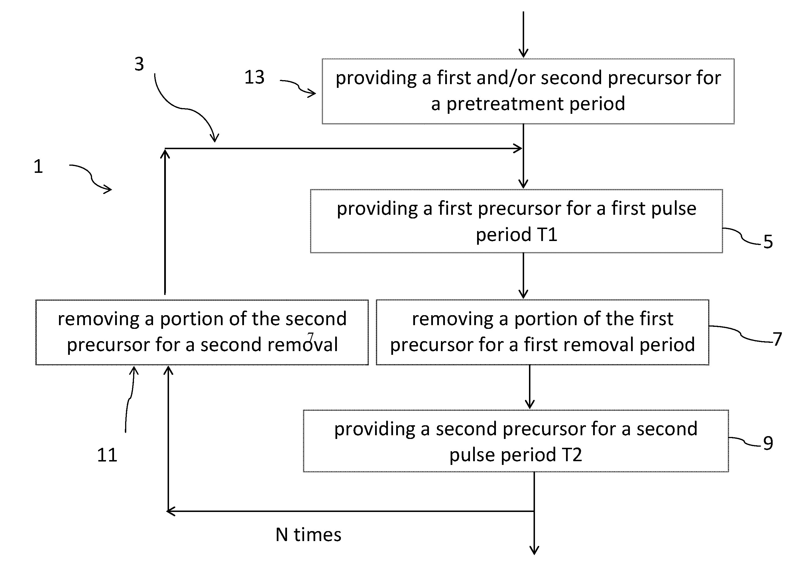
[0029] FIG. 1 shows a flowchart illustrating a method of depositing a layer 1 according to an embodiment. Such method of forming a layer may be N times sequentially repeating a deposition cycle 3 to process a substrate disposed in a reaction chamber. The cycle may comprise supplying 5 a first precursor into the reaction chamber for a first pulse period T1 and removing 7 a portion of the first precursor from the reaction chamber for a first removal period R1. Further the cycle may comprise supplying 9 a second precursor into the reaction chamber for a second pulse period T2 and removing 11 a portion of the second precursor from the reaction chamber for a second removal period R2. A portion of the first and second precursor may form at least a portion of the layer on the substrate.
[0030] The precursors may be gasses, which may be vaporized liquids, which react with each other. The uniformity of the deposited layer on the substrate may be very important. For example, the thickness of the deposited layer over the substrate should be substantially the same over the surface of the substrate for a good uniformity. Further if multiple substrates are processed simultaneously the uniformity of all the different wafers should be the same.
[0031] To improve the uniformity at least one of the first and second precursors may be supplied into the reaction chamber for a pretreatment period 13 longer than the first or second cycle period before sequentially repeating the cycles. The first and second precursor may react into byproducts in the reaction chamber. By supplying at least one of the first and second precursor the reaction chamber for the pretreatment period longer than the first or second pulse period a higher concentration of the byproduct may be generated over a longer period. The byproduct may be more uniformly spread through the reaction chamber during the pretreatment period. Since byproducts may play an important role in preparing the bare surface for deposition of the first, nucleation layer, the uniformity of the nucleation layer may be improved when the byproduct may be better spread through the reaction chamber during the pretreatment period. The uniformity of the first nucleation layer may have a large influence on the uniformity and therefore the quality of the deposited layer.
[0032] It may be that, during the pretreatment period 13, the surface may be prepared for the nucleation layer and that no actual nucleation layer is deposited. For example, if only one of the first and second precursor is provided, the reaction forming the layer may not be initiated. It may also be that, during the pretreatment period, a thin nucleation layer may be deposited.
[0033] The pretreatment may be beneficial when the reactivity of the bare substrate is different than the deposited layer. The mix of reactant during the pretreatment may deposit a nucleation layer or prepare the base surface for improved deposition. Therefore a delay of the deposition process on the substrate may be circumvented and the uniformity improved.
[0034] The pretreatment period 13 may be between 2 to 1200, preferably 8 to 300, more preferably 12 to 100 and most preferably between 15 and 40 times longer than the first or second pulse periods. The pretreatment period may be between 1 to 60, preferably 2 to 40, more preferably 5 to 20 and most preferably 8 to 15 minutes. The exact time of the pretreatment period may be calibrated by varying the pretreatment periods and measuring the uniformity of the deposited layers to select the optimal pretreatment period.
[0035] Sequentially repeating the deposition cycle takes between 1 to 180, preferably 10 to 140 more preferably 20 to 100 and most preferably 40 to 80 minutes. The first and second pulse period 5, 9 may take 1 to 180, preferably 5 to 120, more preferably 8 to 80 and most preferably 10 to 50 seconds. The first and second pulse period may be the same or they may be different. The first pulse period may be longer than the second pulse period.
[0036] The pressure in the reaction chamber is between 0.1 and 1000, preferably 1 and 100, and more preferably 6 and 60 Pa during the pretreatment period 13 and/or the deposition period. The temperature may be between 300 and 900, preferably 500 and 800, more preferably 600 to 700.degree. C.
[0037] The first precursor may comprise a silicon halide. The silicon halide may comprises fluorine (F), chlorine (Cl), bromine (Br), or iodine (I). At least some of the suitable first precursors may have the following general formula:
H.sub.2n+2-ySi.sub.nX.sub.y
[0038] wherein, n=1-10, y=1 or more (and up to 2n+2), and X is F, Cl, I or Br and more preferably n=1-3 and most preferably 1-2. The silicon halide may be a chlorosilane, dichlorosilane (DCS), trichlorosilane, tetrachlorosilane, iodosilane, diiodosilane, tribromosilane, silicic acid, tetraiodosilane, tetrabromosilane, tetrafluorosilane, chlorotrifluorosilane, dichlorodifluorosilane, or a trichlorofluorosilanedichlorsilane.
[0039] The second precursor may comprise a nitriding gas such as for example hydronitrogens. The hydronitrogens may be ammonia (NH.sub.3) or hydrazine (N.sub.2H.sub.4). The second precursor may be activated by plasma-excitation or not.
[0040] The second precursor may comprises an oxidizing gas such as for example oxygen, water or hydrogenperoxide. The terms first or second precursor are not intended to refer to the order in which the precursor are supplied to the reaction chamber. One could start with the second precursor and then continue with the first precursor without adversely affecting the deposited layer.
[0041] The first precursor may be supplied to the reaction chamber between 1 and 20, preferably 1.5 and 4, and more preferably between 2 to 3 times longer than the second precursor during the deposition cycle 3. In this way the stoichiometry of the deposited layer may be varied.
[0042] Both the first and second precursor may also be supplied into the reaction chamber simultaneously for the pretreatment period 13 and a thin nucleation layer may be deposited. The thin layer may be one monolayer thick.
[0043] It may however also be the case that both the first and second precursor may also be supplied into the reaction chamber simultaneously for the pretreatment period 13 and no thin nucleation layer may be deposited. The later may depend on the length of the pretreatment period and other process parameters.
[0044] The first precursor may be removed from the reaction chamber for a first removal period R1 and the second precursor may be removed from the reaction chamber for a second removal period R2 during the deposition cycle. The first and/or second removal period may be between 1 to 120, preferably 5 to 60 more preferably 10 to 30 and most preferably 20 to 40 seconds. The first and/or second precursor may be removed with a pump. A purge gas may be provided during removing the first and/or second precursor from the reaction chamber.
[0045] The amount of the second precursor supplied to the reaction chamber may be between 1 and 25, preferably between 2 to 15 times more than the first precursor supplied to the reaction chamber during sequentially repeating the deposition cycles. In this way the stoichiometry of the deposited layer may be varied.
[0046] The deposition cycles may be repeated between 2 to 100, preferably 10 to 60, and more preferably 20 to 50 times. In this way a layer of the required thickness may be deposited.
[0047] The silicon concentration in the deposited layer of SiN may be between 1 to 25 or even 33% higher than stoichiometric concentration of silicon in Si.sub.3N.sub.4. Such a layer may have a decreased stress level with respect to stoichiometric Si.sub.3N.sub.4.
[0048] The first and second precursor may react with each other to form the layer on the substrate in an atomic layer deposition (ALD) process. In this way the layer may have the benefits from the ALD process. For example a lower hydrogen and chloride content may be found in the ALD deposited layer because there is a bit more time in the ALD process to remove the hydrogen from the layer. Due to less impurities, the quality of the ALD deposited SiN layer, such as the wet etch rate may be better at the same temperature. Also the ALD process may create a silicon nitride layer with an improved conformality to prefabricated features on the substrate. The nucleation of the ALD process may also benefit from the continuous supply of at least one of the and second precursors in the pretreatment period.
[0049] A dopant may be provided to alter the properties of the deposited layer. The dopant may comprises carbon, such as for example CH.sub.4, C.sub.2H.sub.2, C.sub.2H.sub.4. The dopant may be oxygen-containing chemical species, for example oxidizing species such as oxygen (O.sub.2) and oxygen-containing compounds, including NO, N.sub.2O, NO.sub.2, CO.sub.2, H.sub.2O, and alcohols. In some embodiments, the dopant may be PH.sub.3, AsH.sub.3, and SbH.sub.3.
[0050] The layer may be deposited with a deposition apparatus comprising:
[0051] a reaction chamber constructed and arranged to hold at least a first substrate;
[0052] a gas distribution and removal system to provide to and remove from the reaction chamber a first or second precursor; and,
[0053] a sequence controller operably connected to the gas distribution and removal system and comprising a memory provided with a program to execute deposition of a material on the substrate with the gas distribution and removal system by: [0054] sequentially repeating a deposition cycle to deposit at least a portion of the layer on the substrate disposed in the reaction chamber, the cycle comprising: [0055] supplying a first precursor into the reaction chamber for a first pulse period; [0056] removing a portion of the first precursor from the reaction chamber; [0057] supplying a second precursor into the reaction chamber for a second pulse period, and [0058] removing a portion of the second precursor from the reaction chamber;
[0059] wherein the program in the memory is further programmed to control the gas distribution and removal system to supply at least one of the first and second precursors into the reaction chamber for a pretreatment period longer than the first or second pulse period before sequentially repeating the deposition cycles.
[0060] The method may be performed in a vertical furnace. For example, the deposition processes may be performed in an A412.TM. vertical furnace available from ASM International N.V. of Almere, the Netherlands. The furnace has a process chamber that can accommodate a load of 100 to 200 semiconductor substrates, or wafers, having a diameter of 300 mm, with the substrates held in a wafer boat. The program may be programmed via the user interface of the vertical furnace to supply at least one of the first and second precursors into the reaction chamber for a pretreatment period longer than the first or second cycle period before sequentially repeating the ALD cycles.
[0061] An example of a process for the deposition of the silicon nitride may have the following conditions as depicted in table 1:
TABLE-US-00001 TABLE 1 According Process name Reference to embodiment Pre-treatment No DCS/NH3 Pretreatment period (s) 600 Pressure (Pa) 26 NH3 flow (sccm) 300 DCS flow (sccm) 60 N2 flow (sccm) 30 Pulse DCS First pulse time (s) 40 40 Pressure (Pa) 13 13 DCS flow (sccm) 200 200 N2 flow (sccm) 30 30 Pulse NH3 Second pulse time (s) 15 15 Pressure (Pa) 13 13 NH3 flow (sccm) 250 250 N2 flow (sccm) 30 30 Purge pulse Pressure (Pa) 26 26 N2 flow (sccm) 1000 1000 Temperature .degree. C. 650 650 uniformity of the thickness over the substrate 2 0.4 for the worst substrate (.ANG.). uniformity of the thickness over the substrate 0.4 0.4 for the best substrate (.ANG.).
[0062] It will be appreciated by those skilled in the art that various omissions, additions and modifications can be made to the processes and structures described above without departing from the scope of the invention. It is contemplated that various combinations or sub-combinations of the specific features and aspects of the embodiments may be made and still fall within the scope of the description. Various features and aspects of the disclosed embodiments can be combined with, or substituted for, one another in order. All such modifications and changes are intended to fall within the scope of the invention, as defined by the appended claims.
* * * * *
D00000
D00001
XML
uspto.report is an independent third-party trademark research tool that is not affiliated, endorsed, or sponsored by the United States Patent and Trademark Office (USPTO) or any other governmental organization. The information provided by uspto.report is based on publicly available data at the time of writing and is intended for informational purposes only.
While we strive to provide accurate and up-to-date information, we do not guarantee the accuracy, completeness, reliability, or suitability of the information displayed on this site. The use of this site is at your own risk. Any reliance you place on such information is therefore strictly at your own risk.
All official trademark data, including owner information, should be verified by visiting the official USPTO website at www.uspto.gov. This site is not intended to replace professional legal advice and should not be used as a substitute for consulting with a legal professional who is knowledgeable about trademark law.