Technologies For Auto-migration In Accelerated Architectures
Bernat; Francesc Guim ; et al.
U.S. patent application number 15/859385 was filed with the patent office on 2019-02-28 for technologies for auto-migration in accelerated architectures. The applicant listed for this patent is Intel Corporation. Invention is credited to Susanne M. Balle, Francesc Guim Bernat, Evan Custodio, Ramamurthy Krithivas, Karthik Kumar.
| Application Number | 20190065281 15/859385 |
| Document ID | / |
| Family ID | 65434219 |
| Filed Date | 2019-02-28 |
View All Diagrams
| United States Patent Application | 20190065281 |
| Kind Code | A1 |
| Bernat; Francesc Guim ; et al. | February 28, 2019 |
TECHNOLOGIES FOR AUTO-MIGRATION IN ACCELERATED ARCHITECTURES
Abstract
Technologies for auto-migration in accelerated architectures include multiple compute sleds, accelerator sleds, and storage sleds. Each of the compute sleds includes phase detection logic to receive an indication from an application presently executing on the compute sled that indicates a compute kernel associated with the application has been offloaded to a field-programmable gate array (FPGA) of an accelerator sled. The phase detection logic is further to monitor a plurality of hardware threads associated with the application, detect whether a phase change has been detected as a function of the monitored hardware threads, and migrate, in response to having detected the phase change, the hardware threads to another compute element having a lower-performance central processing unit (CPU) relative to the CPU the application is presently being executed on. Other embodiments are described herein.
| Inventors: | Bernat; Francesc Guim; (Barcelona, ES) ; Custodio; Evan; (Seekonk, MA) ; Balle; Susanne M.; (Hudson, NJ) ; Krithivas; Ramamurthy; (Chandler, AZ) ; Kumar; Karthik; (Chandler, AZ) | ||||||||||
| Applicant: |
|
||||||||||
|---|---|---|---|---|---|---|---|---|---|---|---|
| Family ID: | 65434219 | ||||||||||
| Appl. No.: | 15/859385 | ||||||||||
| Filed: | December 30, 2017 |
Related U.S. Patent Documents
| Application Number | Filing Date | Patent Number | ||
|---|---|---|---|---|
| 62584401 | Nov 10, 2017 | |||
| Current U.S. Class: | 1/1 |
| Current CPC Class: | B25J 15/0014 20130101; H04L 43/0876 20130101; G06F 9/4856 20130101; G06F 13/4022 20130101; H04L 41/5025 20130101; G06F 1/183 20130101; G06F 9/505 20130101; H05K 7/1489 20130101; G06F 2200/201 20130101; G06F 2201/86 20130101; G06F 21/105 20130101; G06F 15/7867 20130101; Y02D 30/00 20180101; G06F 11/3006 20130101; G06F 1/20 20130101; Y02D 10/00 20180101; H04L 41/5019 20130101; H04L 49/40 20130101; G06F 15/7807 20130101; G06F 11/3442 20130101; G06N 3/063 20130101; H04L 63/0428 20130101; G06Q 10/0631 20130101; H04L 67/1008 20130101; H04L 41/14 20130101; H04L 41/0896 20130101; H05K 7/20736 20130101; H04L 43/065 20130101; G06F 11/3466 20130101; H04L 41/0816 20130101; G06Q 30/0283 20130101; H05K 7/1498 20130101; G06F 9/5061 20130101; G06F 9/5088 20130101; G06F 11/3409 20130101; H04L 43/16 20130101; H05K 7/18 20130101; G06F 9/44 20130101; G06F 2201/885 20130101; H04L 41/044 20130101 |
| International Class: | G06F 9/50 20060101 G06F009/50; H04L 29/08 20060101 H04L029/08; H04L 12/26 20060101 H04L012/26 |
Foreign Application Data
| Date | Code | Application Number |
|---|---|---|
| Aug 30, 2017 | IN | 201741030632 |
Claims
1. A compute sled for auto-migration in accelerated architectures, the compute sled comprising: a communication circuit; and a compute engine to: receive, from an application executed on a first compute element of a compute sled of a plurality of compute sleds, an indication that a compute kernel associated with the application has been offloaded to a field-programmable gate array (FPGA) of an accelerator sled of a plurality of accelerator sleds, wherein each of the plurality of accelerator sleds and the plurality of compute sleds are communicatively coupled to the compute sled; monitor a plurality of hardware threads associated with the application; detect whether a phase change has been detected as a function of the monitored hardware threads; and migrate, in response to detected detection of the phase change, the hardware threads to a second compute element.
2. The compute sled of claim 1, wherein to monitor the plurality of hardware threads comprises to collect telemetry data corresponding to one or more hardware resources used by the hardware threads during execution, wherein to collect the telemetry data includes to collect an instructions per cycle (IPC) value of the first compute element, and wherein to detect whether the phase change has been detected comprises to compare the IPC value of the first compute element to a peak IPC threshold value.
3. The compute sled of claim 1, wherein to detect whether the phase change has been detected comprises to identify a previous phase as a central processing unit (CPU) bound phase and identify a present phase as one of a FPGA bound phase or a memory bound phase.
4. The compute sled of claim 1, wherein the first compute element on which the application is presently executing comprises a high-performance central processing unit (CPU), and wherein to migrate the hardware threads to the second compute element in response to having detected the phase change comprises to migrate the hardware threads to another high-performance CPU of the compute sled.
5. The compute sled of claim 1, wherein the first compute element on which the application is presently executing comprises a high-performance central processing unit (CPU), and wherein to migrate the hardware threads to the second compute element in response to having detected the phase change comprises to migrate the hardware threads to a high-performance CPU of another compute sled of the plurality of compute sleds.
6. The compute sled of claim 1, wherein the first compute element on which the application is presently executing comprises a high-performance central processing unit (CPU), and wherein to migrate the hardware threads to the second compute element in response to having detected the phase change comprises to migrate the hardware threads to a low-performance CPU of another compute sled of the plurality of compute sleds.
7. The compute sled of claim 1, wherein the first compute element on which the application is presently executing comprises a high-performance central processing unit (CPU), and wherein to migrate the hardware threads to the second compute element in response to having detected the phase change comprises to migrate the hardware threads to a low-performance CPU of the accelerator sled.
8. The compute sled of claim 1, wherein the first compute element on which the application is presently executing comprises a high-performance central processing unit (CPU), and wherein to migrate the hardware threads to the second compute element in response to having detected the phase change comprises to migrate the hardware threads to a low-performance CPU of another accelerator sled of the plurality of accelerator sleds.
9. The compute sled of claim 1, wherein to migrate the hardware threads to the second compute element comprises to pause the hardware threads at the first compute element, migrate states of the hardware threads from the first compute element to the second compute element, resume the migrated hardware threads at the second compute element, and offline the first compute element.
10. The compute sled of claim 1, wherein the compute engine is further to migrate the compute kernel to another FPGA of another accelerator sled of the plurality of accelerator sleds.
11. The compute sled of claim 1, wherein the compute engine is further to: receive an indication that indicates the compute kernel has completed; and migrate, in response to having received the indication, the application to a high-performance CPU of one of the plurality of compute sleds.
12. One or more machine-readable storage media comprising a plurality of instructions stored thereon that, in response to being executed, cause a compute sled to: receive, from an application executed on a first compute element of a compute sled of a plurality of compute sleds, an indication that a compute kernel associated with the application has been offloaded to a field-programmable gate array (FPGA) of an accelerator sled of a plurality of accelerator sleds, wherein each of the plurality of accelerator sleds and the plurality of compute sleds are communicatively coupled to the compute sled; monitor a plurality of hardware threads associated with the application; detect whether a phase change has been detected as a function of the monitored hardware threads; and migrate, in response to detected detection of the phase change, the hardware threads to a second compute element.
13. The one or more machine-readable storage media of claim 12, wherein to monitor the plurality of hardware threads comprises to collect telemetry data corresponding to one or more hardware resources used by the hardware threads during execution, wherein to collect the telemetry data includes to collect an instructions per cycle (IPC) value of the first compute element, and wherein to detect whether the phase change has been detected comprises to compare the IPC value of the first compute element to a peak IPC threshold value.
14. The one or more machine-readable storage media of claim 12, wherein to detect whether the phase change has been detected comprises to identify a previous phase as a central processing unit (CPU) bound phase and identify a present phase as one of a FPGA bound phase or a memory bound phase.
15. The one or more machine-readable storage media of claim 12, wherein the first compute element on which the application is presently executing comprises a high-performance central processing unit (CPU), and wherein to migrate the hardware threads to the second compute element in response to having detected the phase change comprises to migrate the hardware threads to another high-performance CPU of the compute sled.
16. The one or more machine-readable storage media of claim 12, wherein the first compute element on which the application is presently executing comprises a high-performance central processing unit (CPU), and wherein to migrate the hardware threads to the second compute element in response to having detected the phase change comprises to migrate the hardware threads to a high-performance CPU of another compute sled of the plurality of compute sleds.
17. The one or more machine-readable storage media of claim 12, wherein the first compute element on which the application is presently executing comprises a high-performance central processing unit (CPU), and wherein to migrate the hardware threads to the second compute element in response to having detected the phase change comprises to migrate the hardware threads to a low-performance CPU of another compute sled of the plurality of compute sleds.
18. The one or more machine-readable storage media of claim 12, wherein the first compute element on which the application is presently executing comprises a high-performance central processing unit (CPU), and wherein to migrate the hardware threads to the second compute element in response to having detected the phase change comprises to migrate the hardware threads to a low-performance CPU of the accelerator sled.
19. The one or more machine-readable storage media of claim 12, wherein the first compute element on which the application is presently executing comprises a high-performance central processing unit (CPU), and wherein to migrate the hardware threads to the second compute element in response to having detected the phase change comprises to migrate the hardware threads to a low-performance CPU of another accelerator sled of the plurality of accelerator sleds.
20. The one or more machine-readable storage media of claim 12, wherein to migrate the hardware threads to the second compute element comprises to pause the hardware threads at the first compute element, migrate states of the hardware threads from the first compute element to the second compute element, resume the migrated hardware threads at the second compute element, and offline the first compute element.
21. The one or more machine-readable storage media of claim 12, wherein the plurality of instructions further cause the compute sled to migrate the compute kernel to another FPGA of another accelerator sled of the plurality of accelerator sleds.
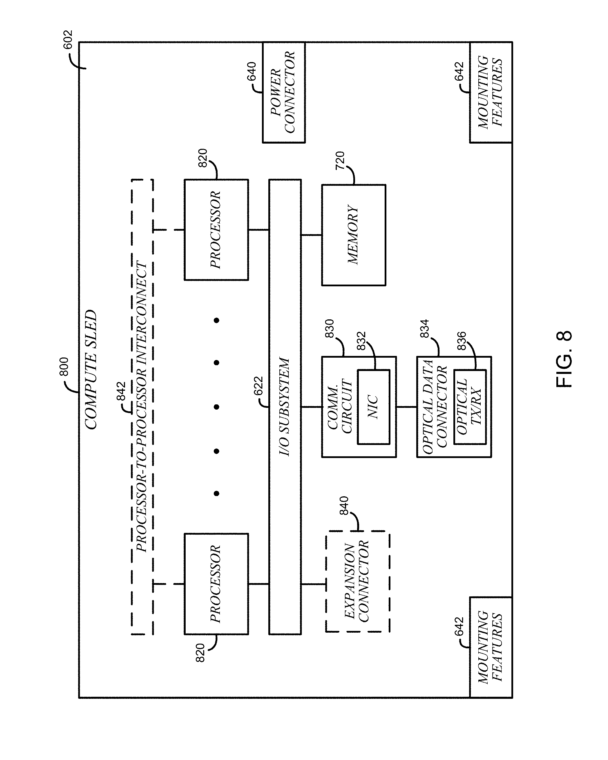
22. The one or more machine-readable storage media of claim 12, wherein the plurality of instructions further cause the compute sled to: receive an indication that indicates the compute kernel has completed; and migrate, in response to having received the indication, the application to a high-performance CPU of one of the plurality of compute sleds.
23. A compute sled for auto-migration in accelerated architectures, the compute sled comprising: circuitry for receiving, from an application executed on a first compute element of a compute sled of a plurality of compute sleds, an indication that a compute kernel associated with the application has been offloaded to a field-programmable gate array (FPGA) of an accelerator sled of a plurality of accelerator sleds, wherein each of the plurality of accelerator sleds and the plurality of compute sleds are communicatively coupled to the compute sled; means for monitoring a plurality of hardware threads associated with the application; means for detecting whether a phase change has been detected as a function of the monitored hardware threads; and circuitry for migrating, in response to detected detection of the phase change, the hardware threads to a second compute element.
24. The compute sled of claim 23, wherein the means for monitoring the plurality of hardware threads comprises means for collecting telemetry data corresponding to one or more hardware resources used by the hardware threads during execution, wherein the means for collecting the telemetry data includes means for collecting an instructions per cycle (IPC) value of the first compute element, and wherein the means for detecting whether the phase change has been detected comprises means for comparing the IPC value of the first compute element to a peak IPC threshold value.
25. The compute sled of claim 23, wherein the means for detecting whether the phase change has been detected comprises means for identifying a previous phase as a central processing unit (CPU) bound phase and identify a present phase as a memory bound phase.
Description
CROSS-REFERENCE TO RELATED APPLICATIONS
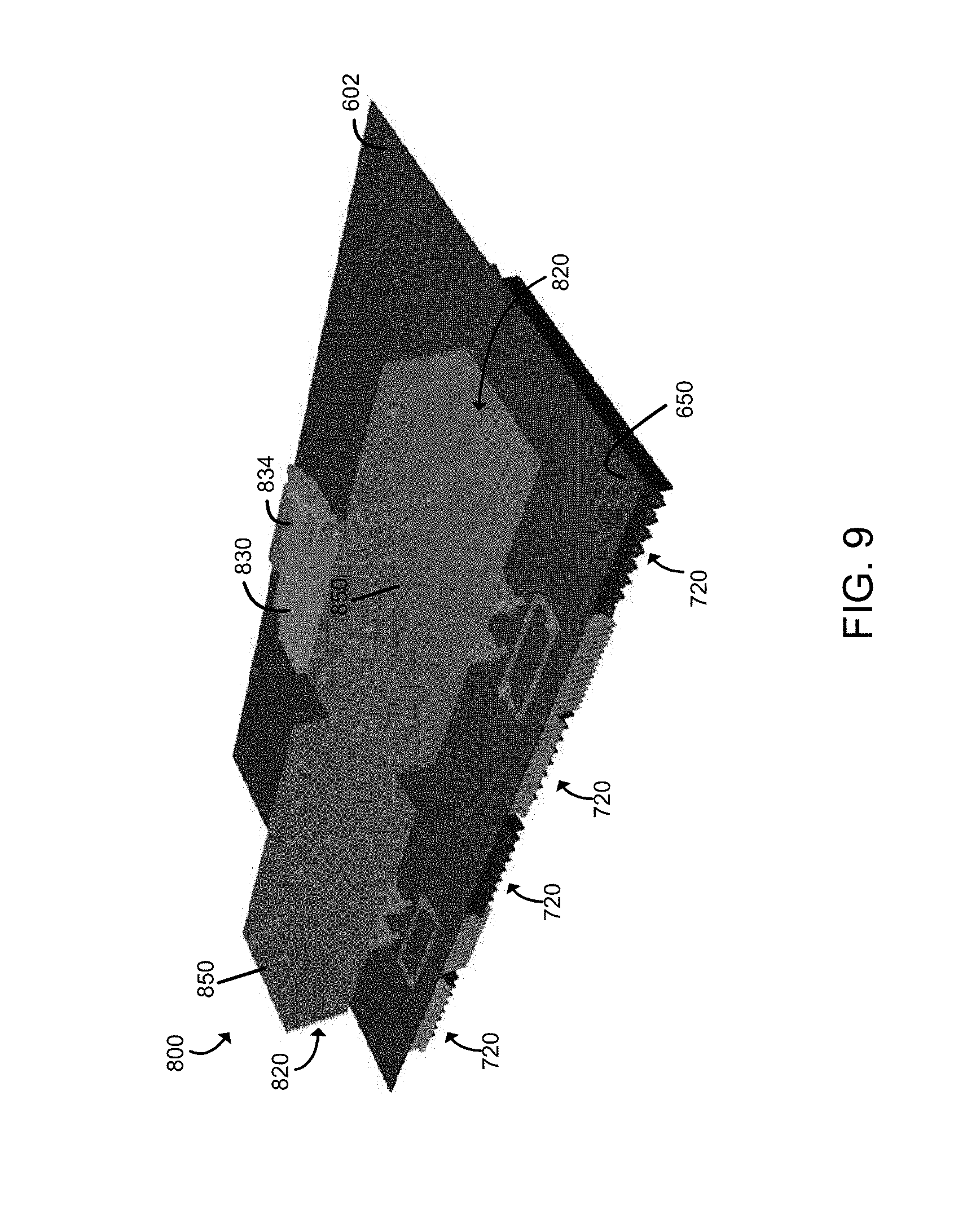
[0001] The present application claims the benefit of Indian Provisional Patent Application No. 201741030632, filed Aug. 30, 2017 and U.S. Provisional Patent Application No. 62/584,401, filed Nov. 10, 2017.
BACKGROUND
[0002] Network operators and service providers typically rely on various accelerator technologies to accelerate workloads in complex, large-scale computing environments, such as high-performance computing (HPC) and cloud computing environments. These accelerators can be configured to perform special purpose computations (e.g., searching, pattern matching, signal- and image-processing, encryption, etc.) in an efficient, parallel manner. One such accelerator technology is a field-programmable gate array (FPGA) consisting of an array of logic gates that can be hardware-programmed to fulfill specific tasks. In particular, the clock cycles of FPGAs are relatively low compared to processor clock rates, which means the FPGAs are generally more power effective relative to processor cores.
[0003] Accordingly, in some computing architectures, while hardware threads of an application are being executed by a processor, certain application functionality (e.g., compute kernels) may be offloaded to an FPGA. Typically, the hardware threads of the application are paused while waiting for the compute kernels to execute in the FPGA. However, because the hardware threads are merely paused, the software stack is required to make the decision to pause/resume, which can be an ineffective solution under certain conditions. Additionally, pausing/resuming the application threads presently works in the order of milliseconds (e.g., driven by software interactions) and consider only a binary solution (i.e., pause/resume), which can be an inflexible solution in certain computing environments.
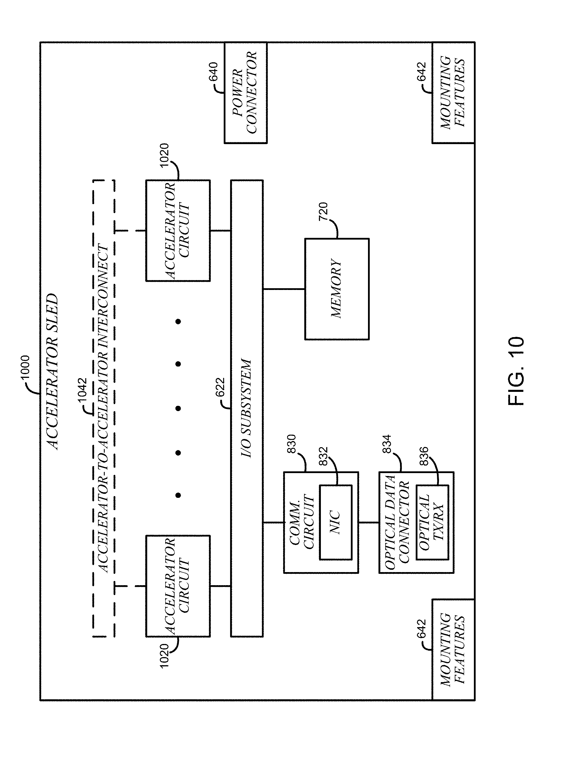
BRIEF DESCRIPTION OF THE DRAWINGS
[0004] The concepts described herein are illustrated by way of example and not by way of limitation in the accompanying figures. For simplicity and clarity of illustration, elements illustrated in the figures are not necessarily drawn to scale. Where considered appropriate, reference labels have been repeated among the figures to indicate corresponding or analogous elements.
[0005] FIG. 1 is a simplified diagram of at least one embodiment of a data center for executing workloads with disaggregated resources;
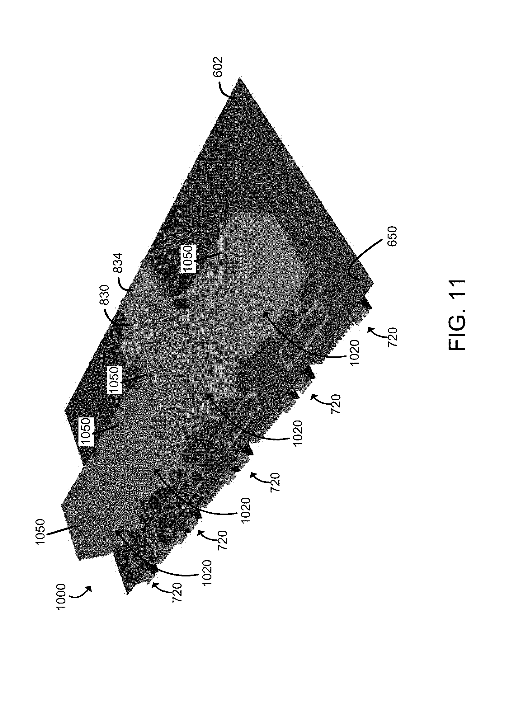
[0006] FIG. 2 is a simplified diagram of at least one embodiment of a pod of the data center of FIG. 1;
[0007] FIG. 3 is a perspective view of at least one embodiment of a rack that may be included in the pod of FIG. 2;
[0008] FIG. 4 is a side plan elevation view of the rack of FIG. 3;
[0009] FIG. 5 is a perspective view of the rack of FIG. 3 having a sled mounted therein;
[0010] FIG. 6 is a is a simplified block diagram of at least one embodiment of a top side of the sled of FIG. 5;
[0011] FIG. 7 is a simplified block diagram of at least one embodiment of a bottom side of the sled of FIG. 6;
[0012] FIG. 8 is a simplified block diagram of at least one embodiment of a compute sled usable in the data center of FIG. 1;
[0013] FIG. 9 is a top perspective view of at least one embodiment of the compute sled of FIG. 8;
[0014] FIG. 10 is a simplified block diagram of at least one embodiment of an accelerator sled usable in the data center of FIG. 1;
[0015] FIG. 11 is a top perspective view of at least one embodiment of the accelerator sled of FIG. 10;
[0016] FIG. 12 is a simplified block diagram of at least one embodiment of a storage sled usable in the data center of FIG. 1;
[0017] FIG. 13 is a top perspective view of at least one embodiment of the storage sled of FIG. 12;
[0018] FIG. 14 is a simplified block diagram of at least one embodiment of a memory sled usable in the data center of FIG. 1; and
[0019] FIG. 15 is a simplified block diagram of a system that may be established within the data center of FIG. 1 to execute workloads with managed nodes composed of disaggregated resources.
[0020] FIG. 16 is a simplified block diagram of at least one embodiment of a system for auto-migration in accelerated architectures which includes multiple compute sleds, a storage sled, multiple accelerator sleds, a network switch, and a resource manager server;
[0021] FIG. 17 is a simplified block diagram of at least one embodiment of one of the compute sleds of the system of FIG. 16;
[0022] FIG. 18 is a simplified block diagram of at least one embodiment of an environment that may be established by one of the compute sleds of FIGS. 16 and 17;
[0023] FIG. 19 is a simplified block diagram of at least one embodiment of the network switch of the system of FIG. 16;
[0024] FIG. 20 is a simplified flow diagram of at least one embodiment of a method for offloading a compute kernel to a field-programmable gate array (FPGA) that may be performed by an application presently executing on one or more compute sleds of the system of FIG. 16;
[0025] FIGS. 21A and 21B are a simplified flow diagram of at least one embodiment of a method for auto-migration in accelerated architectures that may be performed by one of the compute sleds of FIGS. 16-18;
[0026] FIGS. 22A and 22B are simplified block diagrams of at least one embodiment of an auto-migration of an application being consolidated with another application in one of the compute sleds of the system of FIG. 16 having a high-performance central processing unit (CPU);
[0027] FIGS. 23A and 23B are simplified block diagrams of at least one embodiment of an auto-migration of an application being migrated from a high-performance CPU of one of the compute sleds of the system of FIG. 16 to another of the compute sleds having a low-performance CPU; and
[0028] FIGS. 24A and 24B are simplified block diagrams of at least one embodiment of an auto-migration of an application and a compute kernel to one of the accelerator sleds of the system of FIG. 16.
DETAILED DESCRIPTION OF THE DRAWINGS
[0029] While the concepts of the present disclosure are susceptible to various modifications and alternative forms, specific embodiments thereof have been shown by way of example in the drawings and will be described herein in detail. It should be understood, however, that there is no intent to limit the concepts of the present disclosure to the particular forms disclosed, but on the contrary, the intention is to cover all modifications, equivalents, and alternatives consistent with the present disclosure and the appended claims.
[0030] References in the specification to "one embodiment," "an embodiment," "an illustrative embodiment," etc., indicate that the embodiment described may include a particular feature, structure, or characteristic, but every embodiment may or may not necessarily include that particular feature, structure, or characteristic. Moreover, such phrases are not necessarily referring to the same embodiment. Further, when a particular feature, structure, or characteristic is described in connection with an embodiment, it is submitted that it is within the knowledge of one skilled in the art to effect such feature, structure, or characteristic in connection with other embodiments whether or not explicitly described. Additionally, it should be appreciated that items included in a list in the form of "at least one A, B, and C" can mean (A); (B); (C); (A and B); (A and C); (B and C); or (A, B, and C). Similarly, items listed in the form of "at least one of A, B, or C" can mean (A); (B); (C); (A and B); (A and C); (B and C); or (A, B, and C).
[0031] The disclosed embodiments may be implemented, in some cases, in hardware, firmware, software, or any combination thereof. The disclosed embodiments may also be implemented as instructions carried by or stored on a transitory or non-transitory machine-readable (e.g., computer-readable) storage medium, which may be read and executed by one or more processors. A machine-readable storage medium may be embodied as any storage device, mechanism, or other physical structure for storing or transmitting information in a form readable by a machine (e.g., a volatile or non-volatile memory, a media disc, or other media device).
[0032] In the drawings, some structural or method features may be shown in specific arrangements and/or orderings. However, it should be appreciated that such specific arrangements and/or orderings may not be required. Rather, in some embodiments, such features may be arranged in a different manner and/or order than shown in the illustrative figures. Additionally, the inclusion of a structural or method feature in a particular figure is not meant to imply that such feature is required in all embodiments and, in some embodiments, may not be included or may be combined with other features.
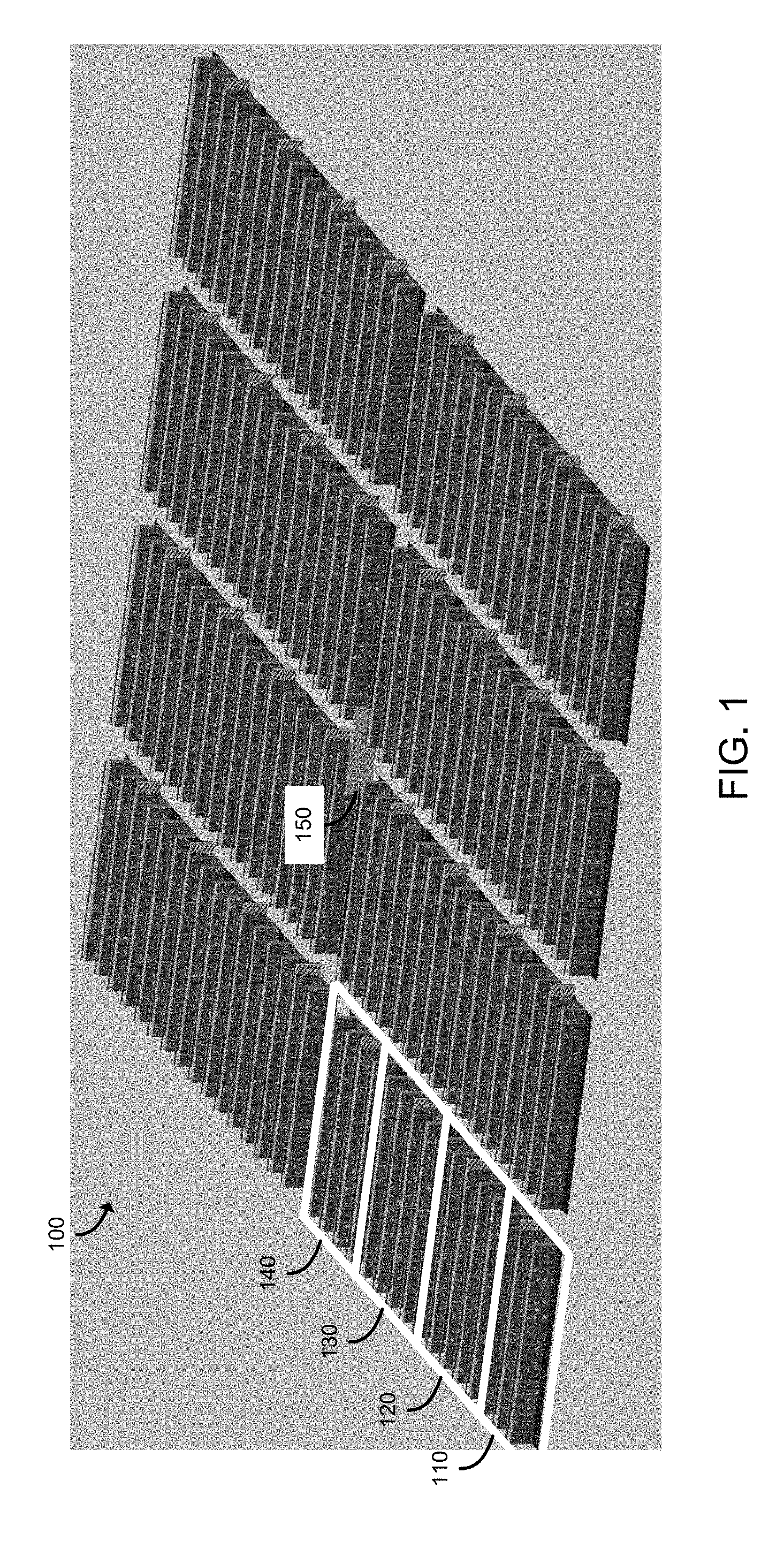
[0033] Referring now to FIG. 1, a data center 100 in which disaggregated resources may cooperatively execute one or more workloads (e.g., applications on behalf of customers) includes multiple pods 110, 120, 130, 140, each of which includes one or more rows of racks. As described in more detail herein, each rack houses multiple sleds, which each may be embodied as a compute device, such as a server, that is primarily equipped with a particular type of resource (e.g., memory devices, data storage devices, accelerator devices, general purpose processors). In the illustrative embodiment, the sleds in each pod 110, 120, 130, 140 are connected to multiple pod switches (e.g., switches that route data communications to and from sleds within the pod). The pod switches, in turn, connect with spine switches 150 that switch communications among pods (e.g., the pods 110, 120, 130, 140) in the data center 100. In some embodiments, the sleds may be connected with a fabric using Intel Omni-Path technology. As described in more detail herein, resources within sleds in the data center 100 may be allocated to a group (referred to herein as a "managed node") containing resources from one or more other sleds to be collectively utilized in the execution of a workload. The workload can execute as if the resources belonging to the managed node were located on the same sled. The resources in a managed node may even belong to sleds belonging to different racks, and even to different pods 110, 120, 130, 140. Some resources of a single sled may be allocated to one managed node while other resources of the same sled are allocated to a different managed node (e.g., one processor assigned to one managed node and another processor of the same sled assigned to a different managed node). By disaggregating resources to sleds comprised predominantly of a single type of resource (e.g., compute sleds comprising primarily compute resources, memory sleds containing primarily memory resources), and selectively allocating and deallocating the disaggregated resources to form a managed node assigned to execute a workload, the data center 100 provides more efficient resource usage over typical data centers comprised of hyperconverged servers containing compute, memory, storage and perhaps additional resources). As such, the data center 100 may provide greater performance (e.g., throughput, operations per second, latency, etc.) than a typical data center that has the same number of resources.
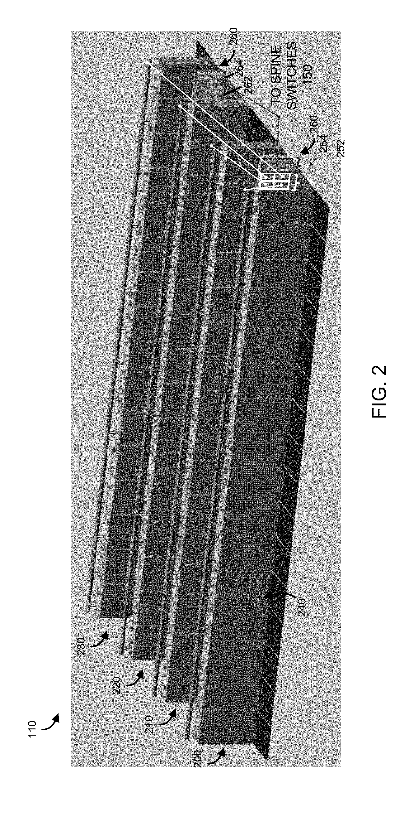
[0034] Referring now to FIG. 2, the pod 110, in the illustrative embodiment, includes a set of rows 200, 210, 220, 230 of racks 240. Each rack 240 may house multiple sleds (e.g., sixteen sleds) and provide power and data connections to the housed sleds, as described in more detail herein. In the illustrative embodiment, the racks in each row 200, 210, 220, 230 are connected to multiple pod switches 250, 260. The pod switch 250 includes a set of ports 252 to which the sleds of the racks of the pod 110 are connected and another set of ports 254 that connect the pod 110 to the spine switches 150 to provide connectivity to other pods in the data center 100. Similarly, the pod switch 260 includes a set of ports 262 to which the sleds of the racks of the pod 110 are connected and a set of ports 264 that connect the pod 110 to the spine switches 150. As such, the use of the pair of switches 250, 260 provides an amount of redundancy to the pod 110. For example, if either of the switches 250, 260 fails, the sleds in the pod 110 may still maintain data communication with the remainder of the data center 100 (e.g., sleds of other pods) through the other switch 250, 260. Furthermore, in the illustrative embodiment, the switches 150, 250, 260 may be embodied as dual-mode optical switches, capable of routing both Ethernet protocol communications carrying Internet Protocol (IP) packets and communications according to a second, high-performance link-layer protocol (e.g., Intel's Omni-Path Architecture's, Infiniband) via optical signaling media of an optical fabric.
[0035] It should be appreciated that each of the other pods 120, 130, 140 (as well as any additional pods of the data center 100) may be similarly structured as, and have components similar to, the pod 110 shown in and described in regard to FIG. 2 (e.g., each pod may have rows of racks housing multiple sleds as described above). Additionally, while two pod switches 250, 260 are shown, it should be understood that in other embodiments, each pod 110, 120, 130, 140 may be connected to different number of pod switches (e.g., providing even more failover capacity).
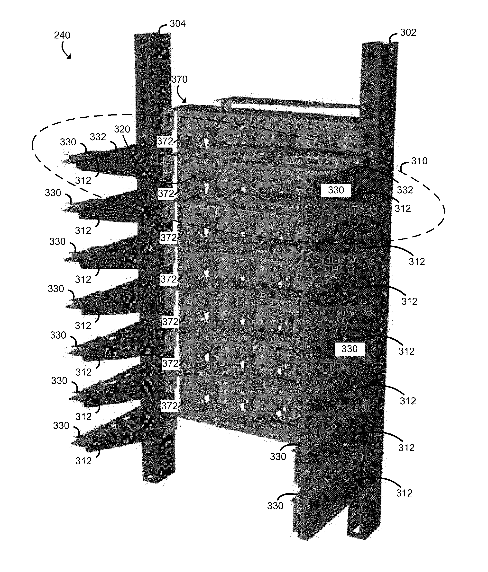
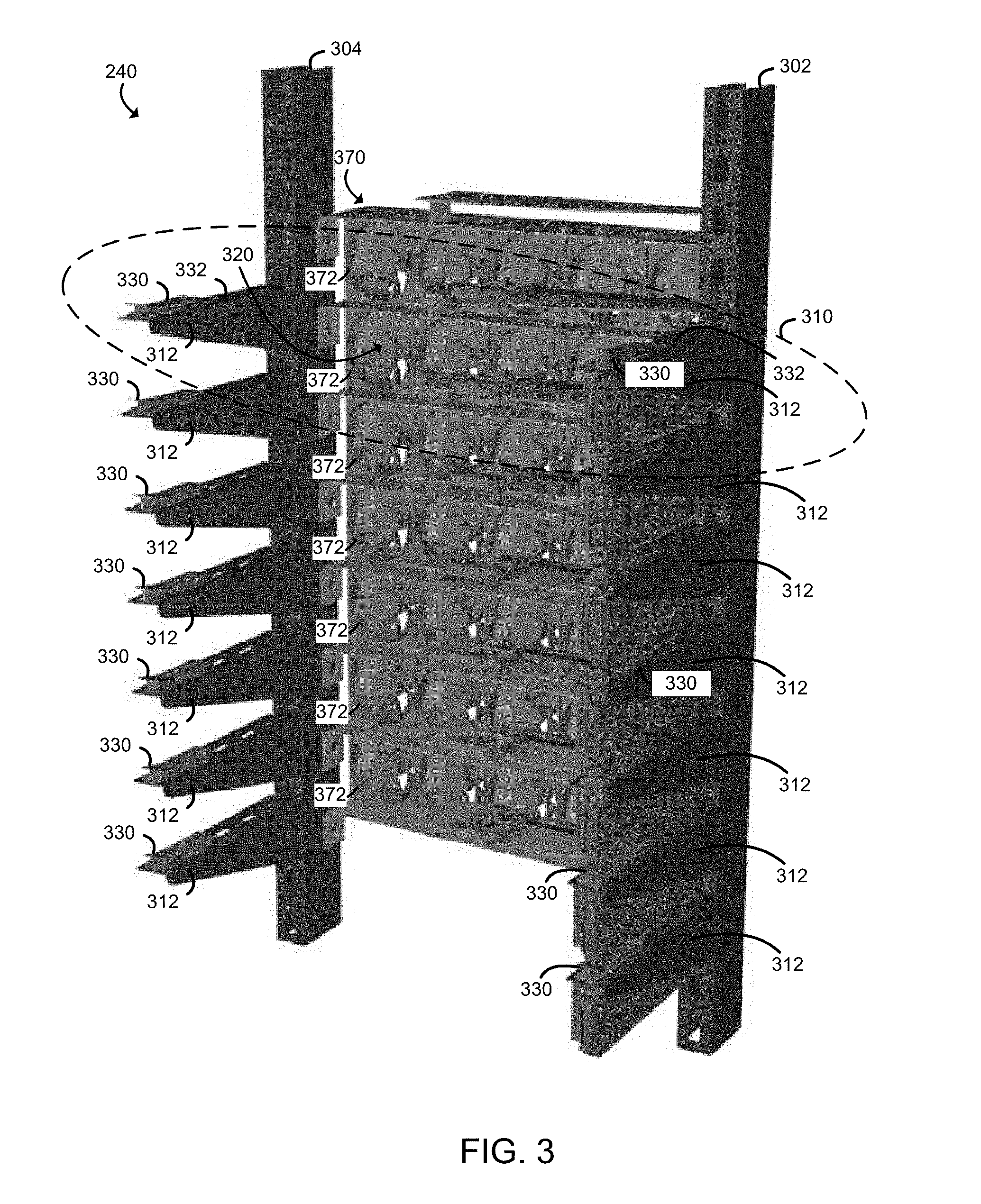
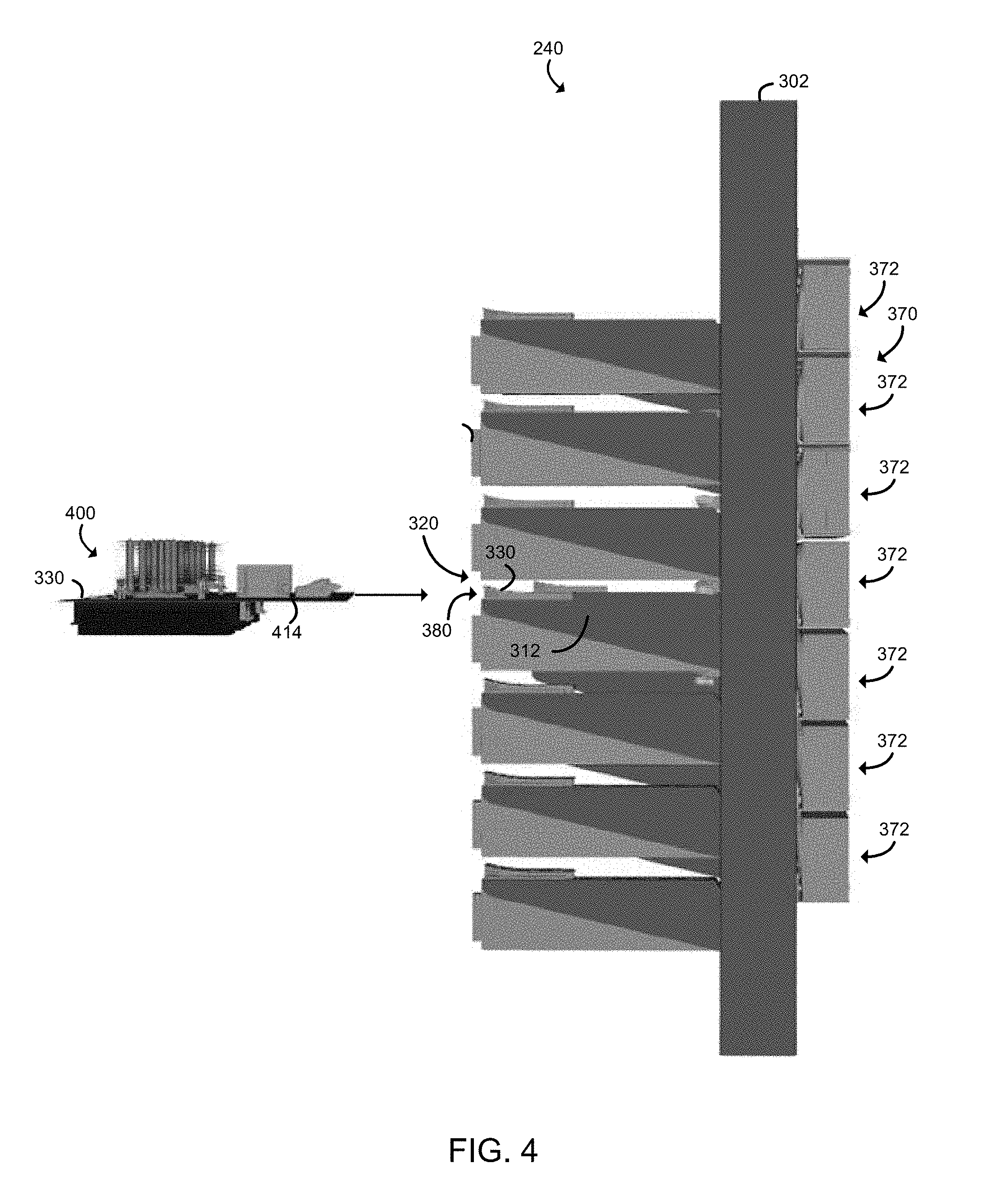
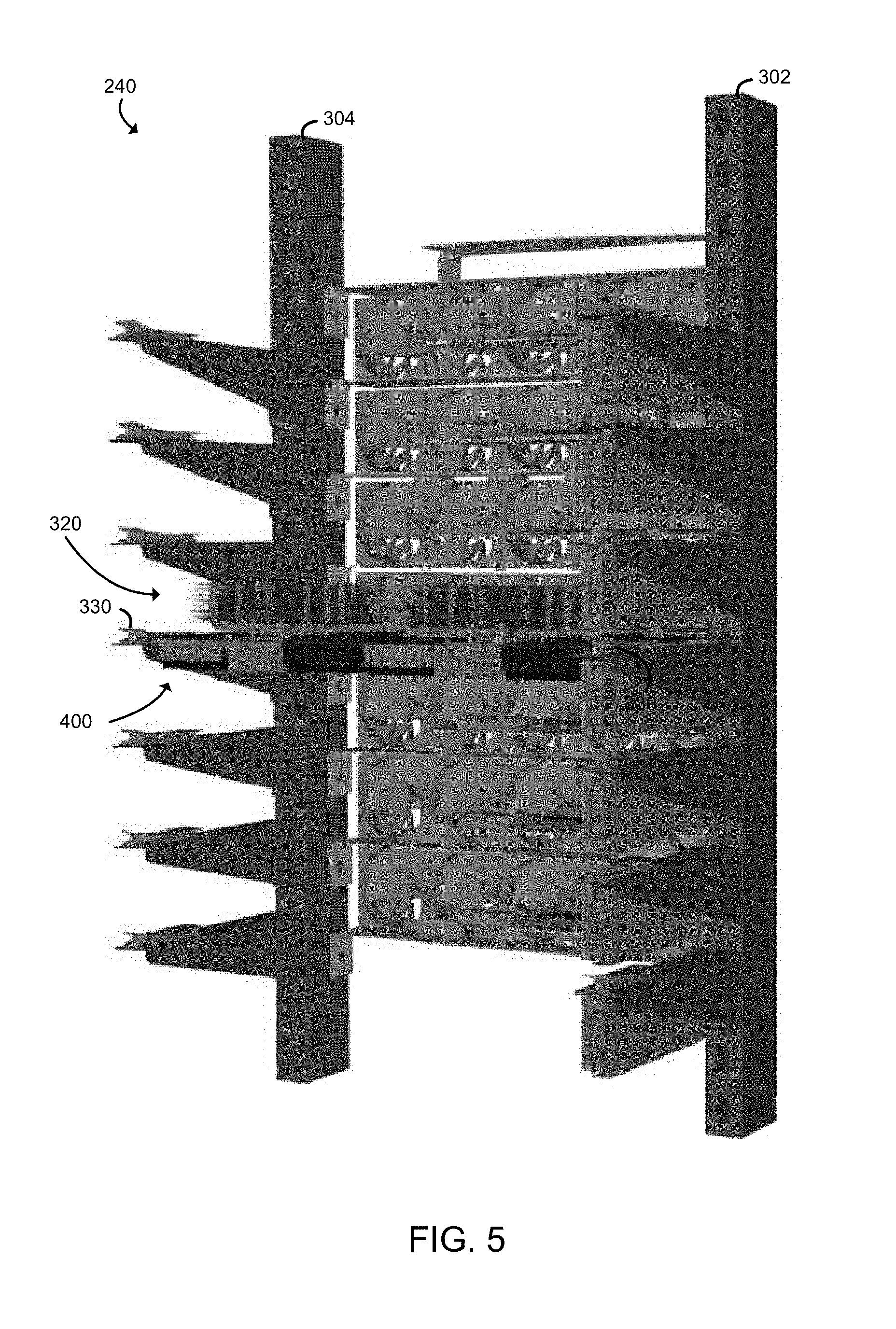
[0036] Referring now to FIGS. 3-5, each illustrative rack 240 of the data center 100 includes two elongated support posts 302, 304, which are arranged vertically. For example, the elongated support posts 302, 304 may extend upwardly from a floor of the data center 100 when deployed. The rack 240 also includes one or more horizontal pairs 310 of elongated support arms 312 (identified in FIG. 3 via a dashed ellipse) configured to support a sled of the data center 100 as discussed below. One elongated support arm 312 of the pair of elongated support arms 312 extends outwardly from the elongated support post 302 and the other elongated support arm 312 extends outwardly from the elongated support post 304.
[0037] In the illustrative embodiments, each sled of the data center 100 is embodied as a chassis-less sled. That is, each sled has a chassis-less circuit board substrate on which physical resources (e.g., processors, memory, accelerators, storage, etc.) are mounted as discussed in more detail below. As such, the rack 240 is configured to receive the chassis-less sleds. For example, each pair 310 of elongated support arms 312 defines a sled slot 320 of the rack 240, which is configured to receive a corresponding chassis-less sled. To do so, each illustrative elongated support arm 312 includes a circuit board guide 330 configured to receive the chassis-less circuit board substrate of the sled. Each circuit board guide 330 is secured to, or otherwise mounted to, a top side 332 of the corresponding elongated support arm 312. For example, in the illustrative embodiment, each circuit board guide 330 is mounted at a distal end of the corresponding elongated support arm 312 relative to the corresponding elongated support post 302, 304. For clarity of the Figures, not every circuit board guide 330 may be referenced in each Figure.
[0038] Each circuit board guide 330 includes an inner wall that defines a circuit board slot 380 configured to receive the chassis-less circuit board substrate of a sled 400 when the sled 400 is received in the corresponding sled slot 320 of the rack 240. To do so, as shown in FIG. 4, a user (or robot) aligns the chassis-less circuit board substrate of an illustrative chassis-less sled 400 to a sled slot 320. The user, or robot, may then slide the chassis-less circuit board substrate forward into the sled slot 320 such that each side edge 414 of the chassis-less circuit board substrate is received in a corresponding circuit board slot 380 of the circuit board guides 330 of the pair 310 of elongated support arms 312 that define the corresponding sled slot 320 as shown in FIG. 4. By having robotically accessible and robotically manipulable sleds comprising disaggregated resources, each type of resource can be upgraded independently of each other and at their own optimized refresh rate. Furthermore, the sleds are configured to blindly mate with power and data communication cables in each rack 240, enhancing their ability to be quickly removed, upgraded, reinstalled, and/or replaced. As such, in some embodiments, the data center 100 may operate (e.g., execute workloads, undergo maintenance and/or upgrades, etc.) without human involvement on the data center floor. In other embodiments, a human may facilitate one or more maintenance or upgrade operations in the data center 100.
[0039] It should be appreciated that each circuit board guide 330 is dual sided. That is, each circuit board guide 330 includes an inner wall that defines a circuit board slot 380 on each side of the circuit board guide 330. In this way, each circuit board guide 330 can support a chassis-less circuit board substrate on either side. As such, a single additional elongated support post may be added to the rack 240 to turn the rack 240 into a two-rack solution that can hold twice as many sled slots 320 as shown in FIG. 3. The illustrative rack 240 includes seven pairs 310 of elongated support arms 312 that define a corresponding seven sled slots 320, each configured to receive and support a corresponding sled 400 as discussed above. Of course, in other embodiments, the rack 240 may include additional or fewer pairs 310 of elongated support arms 312 (i.e., additional or fewer sled slots 320). It should be appreciated that because the sled 400 is chassis-less, the sled 400 may have an overall height that is different than typical servers. As such, in some embodiments, the height of each sled slot 320 may be shorter than the height of a typical server (e.g., shorter than a single rank unit, "1 U"). That is, the vertical distance between each pair 310 of elongated support arms 312 may be less than a standard rack unit "1 U." Additionally, due to the relative decrease in height of the sled slots 320, the overall height of the rack 240 in some embodiments may be shorter than the height of traditional rack enclosures. For example, in some embodiments, each of the elongated support posts 302, 304 may have a length of six feet or less. Again, in other embodiments, the rack 240 may have different dimensions. Further, it should be appreciated that the rack 240 does not include any walls, enclosures, or the like. Rather, the rack 240 is an enclosure-less rack that is opened to the local environment. Of course, in some cases, an end plate may be attached to one of the elongated support posts 302, 304 in those situations in which the rack 240 forms an end-of-row rack in the data center 100.
[0040] In some embodiments, various interconnects may be routed upwardly or downwardly through the elongated support posts 302, 304. To facilitate such routing, each elongated support post 302, 304 includes an inner wall that defines an inner chamber in which the interconnect may be located. The interconnects routed through the elongated support posts 302, 304 may be embodied as any type of interconnects including, but not limited to, data or communication interconnects to provide communication connections to each sled slot 320, power interconnects to provide power to each sled slot 320, and/or other types of interconnects.
[0041] The rack 240, in the illustrative embodiment, includes a support platform on which a corresponding optical data connector (not shown) is mounted. Each optical data connector is associated with a corresponding sled slot 320 and is configured to mate with an optical data connector of a corresponding sled 400 when the sled 400 is received in the corresponding sled slot 320. In some embodiments, optical connections between components (e.g., sleds, racks, and switches) in the data center 100 are made with a blind mate optical connection. For example, a door on each cable may prevent dust from contaminating the fiber inside the cable. In the process of connecting to a blind mate optical connector mechanism, the door is pushed open when the end of the cable enters the connector mechanism. Subsequently, the optical fiber inside the cable enters a gel within the connector mechanism and the optical fiber of one cable comes into contact with the optical fiber of another cable within the gel inside the connector mechanism.
[0042] The illustrative rack 240 also includes a fan array 370 coupled to the cross-support arms of the rack 240. The fan array 370 includes one or more rows of cooling fans 372, which are aligned in a horizontal line between the elongated support posts 302, 304. In the illustrative embodiment, the fan array 370 includes a row of cooling fans 372 for each sled slot 320 of the rack 240. As discussed above, each sled 400 does not include any on-board cooling system in the illustrative embodiment and, as such, the fan array 370 provides cooling for each sled 400 received in the rack 240. Each rack 240, in the illustrative embodiment, also includes a power supply associated with each sled slot 320. Each power supply is secured to one of the elongated support arms 312 of the pair 310 of elongated support arms 312 that define the corresponding sled slot 320. For example, the rack 240 may include a power supply coupled or secured to each elongated support arm 312 extending from the elongated support post 302. Each power supply includes a power connector configured to mate with a power connector of the sled 400 when the sled 400 is received in the corresponding sled slot 320. In the illustrative embodiment, the sled 400 does not include any on-board power supply and, as such, the power supplies provided in the rack 240 supply power to corresponding sleds 400 when mounted to the rack 240.
[0043] Referring now to FIG. 6, the sled 400, in the illustrative embodiment, is configured to be mounted in a corresponding rack 240 of the data center 100 as discussed above. In some embodiments, each sled 400 may be optimized or otherwise configured for performing particular tasks, such as compute tasks, acceleration tasks, data storage tasks, etc. For example, the sled 400 may be embodied as a compute sled 800 as discussed below in regard to FIGS. 8-9, an accelerator sled 1000 as discussed below in regard to FIGS. 10-11, a storage sled 1200 as discussed below in regard to FIGS. 12-13, or as a sled optimized or otherwise configured to perform other specialized tasks, such as a memory sled 1400, discussed below in regard to FIG. 14.
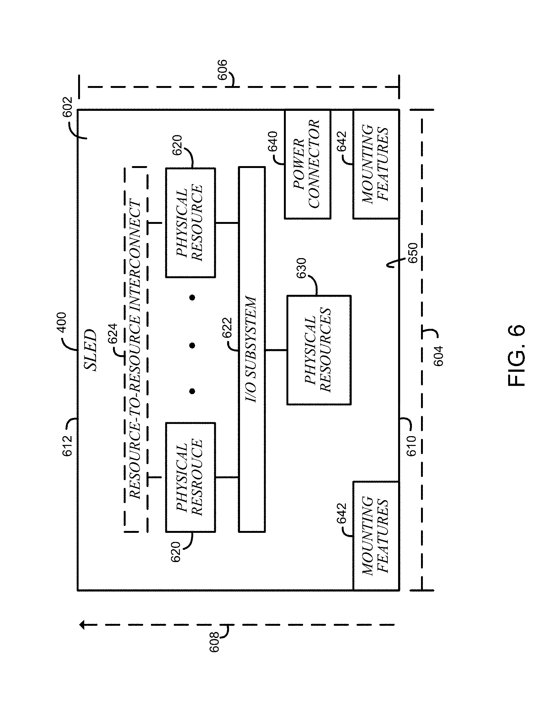
[0044] As discussed above, the illustrative sled 400 includes a chassis-less circuit board substrate 602, which supports various physical resources (e.g., electrical components) mounted thereon. It should be appreciated that the circuit board substrate 602 is "chassis-less" in that the sled 400 does not include a housing or enclosure. Rather, the chassis-less circuit board substrate 602 is open to the local environment. The chassis-less circuit board substrate 602 may be formed from any material capable of supporting the various electrical components mounted thereon. For example, in an illustrative embodiment, the chassis-less circuit board substrate 602 is formed from an FR-4 glass-reinforced epoxy laminate material. Of course, other materials may be used to form the chassis-less circuit board substrate 602 in other embodiments.
[0045] As discussed in more detail below, the chassis-less circuit board substrate 602 includes multiple features that improve the thermal cooling characteristics of the various electrical components mounted on the chassis-less circuit board substrate 602. As discussed, the chassis-less circuit board substrate 602 does not include a housing or enclosure, which may improve the airflow over the electrical components of the sled 400 by reducing those structures that may inhibit air flow. For example, because the chassis-less circuit board substrate 602 is not positioned in an individual housing or enclosure, there is no backplane (e.g., a backplate of the chassis) to the chassis-less circuit board substrate 602, which could inhibit air flow across the electrical components. Additionally, the chassis-less circuit board substrate 602 has a geometric shape configured to reduce the length of the airflow path across the electrical components mounted to the chassis-less circuit board substrate 602. For example, the illustrative chassis-less circuit board substrate 602 has a width 604 that is greater than a depth 606 of the chassis-less circuit board substrate 602. In one particular embodiment, for example, the chassis-less circuit board substrate 602 has a width of about 21 inches and a depth of about 9 inches, compared to a typical server that has a width of about 17 inches and a depth of about 39 inches. As such, an airflow path 608 that extends from a front edge 610 of the chassis-less circuit board substrate 602 toward a rear edge 612 has a shorter distance relative to typical servers, which may improve the thermal cooling characteristics of the sled 400. Furthermore, although not illustrated in FIG. 6, the various physical resources mounted to the chassis-less circuit board substrate 602 are mounted in corresponding locations such that no two substantively heat-producing electrical components shadow each other as discussed in more detail below. That is, no two electrical components, which produce appreciable heat during operation (i.e., greater than a nominal heat sufficient enough to adversely impact the cooling of another electrical component), are mounted to the chassis-less circuit board substrate 602 linearly in-line with each other along the direction of the airflow path 608 (i.e., along a direction extending from the front edge 610 toward the rear edge 612 of the chassis-less circuit board substrate 602).
[0046] As discussed above, the illustrative sled 400 includes one or more physical resources 620 mounted to a top side 650 of the chassis-less circuit board substrate 602. Although two physical resources 620 are shown in FIG. 6, it should be appreciated that the sled 400 may include one, two, or more physical resources 620 in other embodiments. The physical resources 620 may be embodied as any type of processor, controller, or other compute circuit capable of performing various tasks such as compute functions and/or controlling the functions of the sled 400 depending on, for example, the type or intended functionality of the sled 400. For example, as discussed in more detail below, the physical resources 620 may be embodied as high-performance processors in embodiments in which the sled 400 is embodied as a compute sled, as accelerator co-processors or circuits in embodiments in which the sled 400 is embodied as an accelerator sled, storage controllers in embodiments in which the sled 400 is embodied as a storage sled, or a set of memory devices in embodiments in which the sled 400 is embodied as a memory sled.
[0047] The sled 400 also includes one or more additional physical resources 630 mounted to the top side 650 of the chassis-less circuit board substrate 602. In the illustrative embodiment, the additional physical resources include a network interface controller (NIC) as discussed in more detail below. Of course, depending on the type and functionality of the sled 400, the physical resources 630 may include additional or other electrical components, circuits, and/or devices in other embodiments.
[0048] The physical resources 620 are communicatively coupled to the physical resources 630 via an input/output (I/O) subsystem 622. The I/O subsystem 622 may be embodied as circuitry and/or components to facilitate input/output operations with the physical resources 620, the physical resources 630, and/or other components of the sled 400. For example, the I/O subsystem 622 may be embodied as, or otherwise include, memory controller hubs, input/output control hubs, integrated sensor hubs, firmware devices, communication links (e.g., point-to-point links, bus links, wires, cables, light guides, printed circuit board traces, etc.), and/or other components and subsystems to facilitate the input/output operations. In the illustrative embodiment, the I/O subsystem 622 is embodied as, or otherwise includes, a double data rate 4 (DDR4) data bus or a DDRS data bus.
[0049] In some embodiments, the sled 400 may also include a resource-to-resource interconnect 624. The resource-to-resource interconnect 624 may be embodied as any type of communication interconnect capable of facilitating resource-to-resource communications. In the illustrative embodiment, the resource-to-resource interconnect 624 is embodied as a high-speed point-to-point interconnect (e.g., faster than the I/O subsystem 622). For example, the resource-to-resource interconnect 624 may be embodied as a QuickPath Interconnect (QPI), an UltraPath Interconnect (UPI), or other high-speed point-to-point interconnect dedicated to resource-to-resource communications.
[0050] The sled 400 also includes a power connector 640 configured to mate with a corresponding power connector of the rack 240 when the sled 400 is mounted in the corresponding rack 240. The sled 400 receives power from a power supply of the rack 240 via the power connector 640 to supply power to the various electrical components of the sled 400. That is, the sled 400 does not include any local power supply (i.e., an on-board power supply) to provide power to the electrical components of the sled 400. The exclusion of a local or on-board power supply facilitates the reduction in the overall footprint of the chassis-less circuit board substrate 602, which may increase the thermal cooling characteristics of the various electrical components mounted on the chassis-less circuit board substrate 602 as discussed above. In some embodiments, power is provided to the processors 820 through vias directly under the processors 820 (e.g., through the bottom side 750 of the chassis-less circuit board substrate 602), providing an increased thermal budget, additional current and/or voltage, and better voltage control over typical boards.
[0051] In some embodiments, the sled 400 may also include mounting features 642 configured to mate with a mounting arm, or other structure, of a robot to facilitate the placement of the sled 600 in a rack 240 by the robot. The mounting features 642 may be embodied as any type of physical structures that allow the robot to grasp the sled 400 without damaging the chassis-less circuit board substrate 602 or the electrical components mounted thereto. For example, in some embodiments, the mounting features 642 may be embodied as non-conductive pads attached to the chassis-less circuit board substrate 602. In other embodiments, the mounting features may be embodied as brackets, braces, or other similar structures attached to the chassis-less circuit board substrate 602. The particular number, shape, size, and/or make-up of the mounting feature 642 may depend on the design of the robot configured to manage the sled 400.
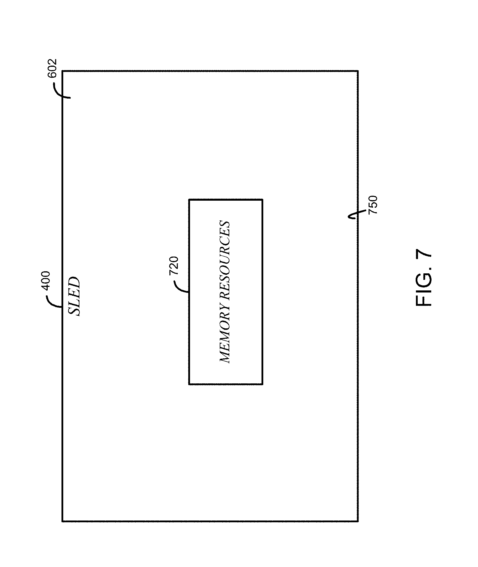
[0052] Referring now to FIG. 7, in addition to the physical resources 630 mounted on the top side 650 of the chassis-less circuit board substrate 602, the sled 400 also includes one or more memory devices 720 mounted to a bottom side 750 of the chassis-less circuit board substrate 602. That is, the chassis-less circuit board substrate 602 is embodied as a double-sided circuit board. The physical resources 620 are communicatively coupled to the memory devices 720 via the I/O subsystem 622. For example, the physical resources 620 and the memory devices 720 may be communicatively coupled by one or more vias extending through the chassis-less circuit board substrate 602. Each physical resource 620 may be communicatively coupled to a different set of one or more memory devices 720 in some embodiments. Alternatively, in other embodiments, each physical resource 620 may be communicatively coupled to each memory devices 720.
[0053] The memory devices 720 may be embodied as any type of memory device capable of storing data for the physical resources 620 during operation of the sled 400, such as any type of volatile (e.g., dynamic random access memory (DRAM), etc.) or non-volatile memory. Volatile memory may be a storage medium that requires power to maintain the state of data stored by the medium. Non-limiting examples of volatile memory may include various types of random access memory (RAM), such as dynamic random access memory (DRAM) or static random access memory (SRAM). One particular type of DRAM that may be used in a memory module is synchronous dynamic random access memory (SDRAM). In particular embodiments, DRAM of a memory component may comply with a standard promulgated by JEDEC, such as JESD79F for DDR SDRAM, JESD79-2F for DDR2 SDRAM, JESD79-3F for DDR3 SDRAM, JESD79-4A for DDR4 SDRAM, JESD209 for Low Power DDR (LPDDR), JESD209-2 for LPDDR2, JESD209-3 for LPDDR3, and JESD209-4 for LPDDR4 (these standards are available at www.jedec.org). Such standards (and similar standards) may be referred to as DDR-based standards and communication interfaces of the storage devices that implement such standards may be referred to as DDR-based interfaces.
[0054] In one embodiment, the memory device is a block addressable memory device, such as those based on NAND or NOR technologies. A memory device may also include next-generation nonvolatile devices, such as Intel 3D XPoint.TM. memory or other byte addressable write-in-place nonvolatile memory devices. In one embodiment, the memory device may be or may include memory devices that use chalcogenide glass, multi-threshold level NAND flash memory, NOR flash memory, single or multi-level Phase Change Memory (PCM), a resistive memory, nanowire memory, ferroelectric transistor random access memory (FeTRAM), anti-ferroelectric memory, magnetoresistive random access memory (MRAM) memory that incorporates memristor technology, resistive memory including the metal oxide base, the oxygen vacancy base and the conductive bridge Random Access Memory (CB-RAM), or spin transfer torque (STT)-MRAM, a spintronic magnetic junction memory based device, a magnetic tunneling junction (MTJ) based device, a DW (Domain Wall) and SOT (Spin Orbit Transfer) based device, a thyristor based memory device, or a combination of any of the above, or other memory. The memory device may refer to the die itself and/or to a packaged memory product. In some embodiments, the memory device may comprise a transistor-less stackable cross point architecture in which memory cells sit at the intersection of word lines and bit lines and are individually addressable and in which bit storage is based on a change in bulk resistance.
[0055] Referring now to FIG. 8, in some embodiments, the sled 400 may be embodied as a compute sled 800. The compute sled 800 is optimized, or otherwise configured, to perform compute tasks. Of course, as discussed above, the compute sled 800 may rely on other sleds, such as acceleration sleds and/or storage sleds, to perform such compute tasks. The compute sled 800 includes various physical resources (e.g., electrical components) similar to the physical resources of the sled 400, which have been identified in FIG. 8 using the same reference numbers. The description of such components provided above in regard to FIGS. 6 and 7 applies to the corresponding components of the compute sled 800 and is not repeated herein for clarity of the description of the compute sled 800.
[0056] In the illustrative compute sled 800, the physical resources 620 are embodied as processors 820. Although only two processors 820 are shown in FIG. 8, it should be appreciated that the compute sled 800 may include additional processors 820 in other embodiments. Illustratively, the processors 820 are embodied as high-performance processors 820 and may be configured to operate at a relatively high power rating. Although the processors 820 generate additional heat operating at power ratings greater than typical processors (which operate at around 155-230 W), the enhanced thermal cooling characteristics of the chassis-less circuit board substrate 602 discussed above facilitate the higher power operation. For example, in the illustrative embodiment, the processors 820 are configured to operate at a power rating of at least 250 W. In some embodiments, the processors 820 may be configured to operate at a power rating of at least 350 W.
[0057] In some embodiments, the compute sled 800 may also include a processor-to-processor interconnect 842. Similar to the resource-to-resource interconnect 624 of the sled 400 discussed above, the processor-to-processor interconnect 842 may be embodied as any type of communication interconnect capable of facilitating processor-to-processor interconnect 842 communications. In the illustrative embodiment, the processor-to-processor interconnect 842 is embodied as a high-speed point-to-point interconnect (e.g., faster than the I/O subsystem 622). For example, the processor-to-processor interconnect 842 may be embodied as a QuickPath Interconnect (QPI), an UltraPath Interconnect (UPI), or other high-speed point-to-point interconnect dedicated to processor-to-processor communications.
[0058] The compute sled 800 also includes a communication circuit 830. The illustrative communication circuit 830 includes a network interface controller (NIC) 832, which may also be referred to as a host fabric interface (HFI). The NIC 832 may be embodied as, or otherwise include, any type of integrated circuit, discrete circuits, controller chips, chipsets, add-in-boards, daughtercards, network interface cards, other devices that may be used by the compute sled 800 to connect with another compute device (e.g., with other sleds 400). In some embodiments, the NIC 832 may be embodied as part of a system-on-a-chip (SoC) that includes one or more processors, or included on a multichip package that also contains one or more processors. In some embodiments, the NIC 832 may include a local processor (not shown) and/or a local memory (not shown) that are both local to the NIC 832. In such embodiments, the local processor of the NIC 832 may be capable of performing one or more of the functions of the processors 820. Additionally or alternatively, in such embodiments, the local memory of the NIC 832 may be integrated into one or more components of the compute sled at the board level, socket level, chip level, and/or other levels.
[0059] The communication circuit 830 is communicatively coupled to an optical data connector 834. The optical data connector 834 is configured to mate with a corresponding optical data connector of the rack 240 when the compute sled 800 is mounted in the rack 240. Illustratively, the optical data connector 834 includes a plurality of optical fibers which lead from a mating surface of the optical data connector 834 to an optical transceiver 836. The optical transceiver 836 is configured to convert incoming optical signals from the rack-side optical data connector to electrical signals and to convert electrical signals to outgoing optical signals to the rack-side optical data connector. Although shown as forming part of the optical data connector 834 in the illustrative embodiment, the optical transceiver 836 may form a portion of the communication circuit 830 in other embodiments.
[0060] In some embodiments, the compute sled 800 may also include an expansion connector 840. In such embodiments, the expansion connector 840 is configured to mate with a corresponding connector of an expansion chassis-less circuit board substrate to provide additional physical resources to the compute sled 800. The additional physical resources may be used, for example, by the processors 820 during operation of the compute sled 800. The expansion chassis-less circuit board substrate may be substantially similar to the chassis-less circuit board substrate 602 discussed above and may include various electrical components mounted thereto. The particular electrical components mounted to the expansion chassis-less circuit board substrate may depend on the intended functionality of the expansion chassis-less circuit board substrate. For example, the expansion chassis-less circuit board substrate may provide additional compute resources, memory resources, and/or storage resources. As such, the additional physical resources of the expansion chassis-less circuit board substrate may include, but is not limited to, processors, memory devices, storage devices, and/or accelerator circuits including, for example, field programmable gate arrays (FPGA), application-specific integrated circuits (ASICs), security co-processors, graphics processing units (GPUs), machine learning circuits, or other specialized processors, controllers, devices, and/or circuits.
[0061] Referring now to FIG. 9, an illustrative embodiment of the compute sled 800 is shown. As shown, the processors 820, communication circuit 830, and optical data connector 834 are mounted to the top side 650 of the chassis-less circuit board substrate 602. Any suitable attachment or mounting technology may be used to mount the physical resources of the compute sled 800 to the chassis-less circuit board substrate 602. For example, the various physical resources may be mounted in corresponding sockets (e.g., a processor socket), holders, or brackets. In some cases, some of the electrical components may be directly mounted to the chassis-less circuit board substrate 602 via soldering or similar techniques.
[0062] As discussed above, the individual processors 820 and communication circuit 830 are mounted to the top side 650 of the chassis-less circuit board substrate 602 such that no two heat-producing, electrical components shadow each other. In the illustrative embodiment, the processors 820 and communication circuit 830 are mounted in corresponding locations on the top side 650 of the chassis-less circuit board substrate 602 such that no two of those physical resources are linearly in-line with others along the direction of the airflow path 608. It should be appreciated that, although the optical data connector 834 is in-line with the communication circuit 830, the optical data connector 834 produces no or nominal heat during operation.
[0063] The memory devices 720 of the compute sled 800 are mounted to the bottom side 750 of the of the chassis-less circuit board substrate 602 as discussed above in regard to the sled 400. Although mounted to the bottom side 750, the memory devices 720 are communicatively coupled to the processors 820 located on the top side 650 via the I/O subsystem 622. Because the chassis-less circuit board substrate 602 is embodied as a double-sided circuit board, the memory devices 720 and the processors 820 may be communicatively coupled by one or more vias, connectors, or other mechanisms extending through the chassis-less circuit board substrate 602. Of course, each processor 820 may be communicatively coupled to a different set of one or more memory devices 720 in some embodiments. Alternatively, in other embodiments, each processor 820 may be communicatively coupled to each memory device 720. In some embodiments, the memory devices 720 may be mounted to one or more memory mezzanines on the bottom side of the chassis-less circuit board substrate 602 and may interconnect with a corresponding processor 820 through a ball-grid array.
[0064] Each of the processors 820 includes a heatsink 850 secured thereto. Due to the mounting of the memory devices 720 to the bottom side 750 of the chassis-less circuit board substrate 602 (as well as the vertical spacing of the sleds 400 in the corresponding rack 240), the top side 650 of the chassis-less circuit board substrate 602 includes additional "free" area or space that facilitates the use of heatsinks 850 having a larger size relative to traditional heatsinks used in typical servers. Additionally, due to the improved thermal cooling characteristics of the chassis-less circuit board substrate 602, none of the processor heatsinks 850 include cooling fans attached thereto. That is, each of the heatsinks 850 is embodied as a fan-less heatsinks.
[0065] Referring now to FIG. 10, in some embodiments, the sled 400 may be embodied as an accelerator sled 1000. The accelerator sled 1000 is optimized, or otherwise configured, to perform specialized compute tasks, such as machine learning, encryption, hashing, or other computational-intensive task. In some embodiments, for example, a compute sled 800 may offload tasks to the accelerator sled 1000 during operation. The accelerator sled 1000 includes various components similar to components of the sled 400 and/or compute sled 800, which have been identified in FIG. 10 using the same reference numbers. The description of such components provided above in regard to FIGS. 6, 7, and 8 apply to the corresponding components of the accelerator sled 1000 and is not repeated herein for clarity of the description of the accelerator sled 1000.
[0066] In the illustrative accelerator sled 1000, the physical resources 620 are embodied as accelerator circuits 1020. Although only two accelerator circuits 1020 are shown in FIG. 10, it should be appreciated that the accelerator sled 1000 may include additional accelerator circuits 1020 in other embodiments. For example, as shown in FIG. 11, the accelerator sled 1000 may include four accelerator circuits 1020 in some embodiments. The accelerator circuits 1020 may be embodied as any type of processor, co-processor, compute circuit, or other device capable of performing compute or processing operations. For example, the accelerator circuits 1020 may be embodied as, for example, field programmable gate arrays (FPGA), application-specific integrated circuits (ASICs), security co-processors, graphics processing units (GPUs), machine learning circuits, or other specialized processors, controllers, devices, and/or circuits.
[0067] In some embodiments, the accelerator sled 1000 may also include an accelerator-to-accelerator interconnect 1042. Similar to the resource-to-resource interconnect 624 of the sled 600 discussed above, the accelerator-to-accelerator interconnect 1042 may be embodied as any type of communication interconnect capable of facilitating accelerator-to-accelerator communications. In the illustrative embodiment, the accelerator-to-accelerator interconnect 1042 is embodied as a high-speed point-to-point interconnect (e.g., faster than the I/O subsystem 622). For example, the accelerator-to-accelerator interconnect 1042 may be embodied as a QuickPath Interconnect (QPI), an UltraPath Interconnect (UPI), or other high-speed point-to-point interconnect dedicated to processor-to-processor communications. In some embodiments, the accelerator circuits 1020 may be daisy-chained with a primary accelerator circuit 1020 connected to the NIC 832 and memory 720 through the I/O subsystem 622 and a secondary accelerator circuit 1020 connected to the NIC 832 and memory 720 through a primary accelerator circuit 1020.
[0068] Referring now to FIG. 11, an illustrative embodiment of the accelerator sled 1000 is shown. As discussed above, the accelerator circuits 1020, communication circuit 830, and optical data connector 834 are mounted to the top side 650 of the chassis-less circuit board substrate 602. Again, the individual accelerator circuits 1020 and communication circuit 830 are mounted to the top side 650 of the chassis-less circuit board substrate 602 such that no two heat-producing, electrical components shadow each other as discussed above. The memory devices 720 of the accelerator sled 1000 are mounted to the bottom side 750 of the of the chassis-less circuit board substrate 602 as discussed above in regard to the sled 600. Although mounted to the bottom side 750, the memory devices 720 are communicatively coupled to the accelerator circuits 1020 located on the top side 650 via the I/O subsystem 622 (e.g., through vias). Further, each of the accelerator circuits 1020 may include a heatsink 1070 that is larger than a traditional heatsink used in a server. As discussed above with reference to the heatsinks 870, the heatsinks 1070 may be larger than tradition heatsinks because of the "free" area provided by the memory devices 750 being located on the bottom side 750 of the chassis-less circuit board substrate 602 rather than on the top side 650.
[0069] Referring now to FIG. 12, in some embodiments, the sled 400 may be embodied as a storage sled 1200. The storage sled 1200 is optimized, or otherwise configured, to store data in a data storage 1250 local to the storage sled 1200. For example, during operation, a compute sled 800 or an accelerator sled 1000 may store and retrieve data from the data storage 1250 of the storage sled 1200. The storage sled 1200 includes various components similar to components of the sled 400 and/or the compute sled 800, which have been identified in FIG. 12 using the same reference numbers. The description of such components provided above in regard to FIGS. 6, 7, and 8 apply to the corresponding components of the storage sled 1200 and is not repeated herein for clarity of the description of the storage sled 1200.
[0070] In the illustrative storage sled 1200, the physical resources 620 are embodied as storage controllers 1220. Although only two storage controllers 1220 are shown in FIG. 12, it should be appreciated that the storage sled 1200 may include additional storage controllers 1220 in other embodiments. The storage controllers 1220 may be embodied as any type of processor, controller, or control circuit capable of controlling the storage and retrieval of data into the data storage 1250 based on requests received via the communication circuit 830. In the illustrative embodiment, the storage controllers 1220 are embodied as relatively low-power processors or controllers. For example, in some embodiments, the storage controllers 1220 may be configured to operate at a power rating of about 75 watts.
[0071] In some embodiments, the storage sled 1200 may also include a controller-to-controller interconnect 1242. Similar to the resource-to-resource interconnect 624 of the sled 400 discussed above, the controller-to-controller interconnect 1242 may be embodied as any type of communication interconnect capable of facilitating controller-to-controller communications. In the illustrative embodiment, the controller-to-controller interconnect 1242 is embodied as a high-speed point-to-point interconnect (e.g., faster than the I/O subsystem 622). For example, the controller-to-controller interconnect 1242 may be embodied as a QuickPath Interconnect (QPI), an UltraPath Interconnect (UPI), or other high-speed point-to-point interconnect dedicated to processor-to-processor communications.
[0072] Referring now to FIG. 13, an illustrative embodiment of the storage sled 1200 is shown. In the illustrative embodiment, the data storage 1250 is embodied as, or otherwise includes, a storage cage 1252 configured to house one or more solid state drives (SSDs) 1254. To do so, the storage cage 1252 includes a number of mounting slots 1256, each of which is configured to receive a corresponding solid state drive 1254. Each of the mounting slots 1256 includes a number of drive guides 1258 that cooperate to define an access opening 1260 of the corresponding mounting slot 1256. The storage cage 1252 is secured to the chassis-less circuit board substrate 602 such that the access openings face away from (i.e., toward the front of) the chassis-less circuit board substrate 602. As such, solid state drives 1254 are accessible while the storage sled 1200 is mounted in a corresponding rack 204. For example, a solid state drive 1254 may be swapped out of a rack 240 (e.g., via a robot) while the storage sled 1200 remains mounted in the corresponding rack 240.
[0073] The storage cage 1252 illustratively includes sixteen mounting slots 1256 and is capable of mounting and storing sixteen solid state drives 1254. Of course, the storage cage 1252 may be configured to store additional or fewer solid state drives 1254 in other embodiments. Additionally, in the illustrative embodiment, the solid state drivers are mounted vertically in the storage cage 1252, but may be mounted in the storage cage 1252 in a different orientation in other embodiments. Each solid state drive 1254 may be embodied as any type of data storage device capable of storing long term data. To do so, the solid state drives 1254 may include volatile and non-volatile memory devices discussed above.
[0074] As shown in FIG. 13, the storage controllers 1220, the communication circuit 830, and the optical data connector 834 are illustratively mounted to the top side 650 of the chassis-less circuit board substrate 602. Again, as discussed above, any suitable attachment or mounting technology may be used to mount the electrical components of the storage sled 1200 to the chassis-less circuit board substrate 602 including, for example, sockets (e.g., a processor socket), holders, brackets, soldered connections, and/or other mounting or securing techniques.
[0075] As discussed above, the individual storage controllers 1220 and the communication circuit 830 are mounted to the top side 650 of the chassis-less circuit board substrate 602 such that no two heat-producing, electrical components shadow each other. For example, the storage controllers 1220 and the communication circuit 830 are mounted in corresponding locations on the top side 650 of the chassis-less circuit board substrate 602 such that no two of those electrical components are linearly in-line with other along the direction of the airflow path 608.
[0076] The memory devices 720 of the storage sled 1200 are mounted to the bottom side 750 of the of the chassis-less circuit board substrate 602 as discussed above in regard to the sled 400. Although mounted to the bottom side 750, the memory devices 720 are communicatively coupled to the storage controllers 1220 located on the top side 650 via the I/O subsystem 622. Again, because the chassis-less circuit board substrate 602 is embodied as a double-sided circuit board, the memory devices 720 and the storage controllers 1220 may be communicatively coupled by one or more vias, connectors, or other mechanisms extending through the chassis-less circuit board substrate 602. Each of the storage controllers 1220 includes a heatsink 1270 secured thereto. As discussed above, due to the improved thermal cooling characteristics of the chassis-less circuit board substrate 602 of the storage sled 1200, none of the heatsinks 1270 include cooling fans attached thereto. That is, each of the heatsinks 1270 is embodied as a fan-less heatsink.
[0077] Referring now to FIG. 14, in some embodiments, the sled 400 may be embodied as a memory sled 1400. The storage sled 1400 is optimized, or otherwise configured, to provide other sleds 400 (e.g., compute sleds 800, accelerator sleds 1000, etc.) with access to a pool of memory (e.g., in two or more sets 1430, 1432 of memory devices 720) local to the memory sled 1200. For example, during operation, a compute sled 800 or an accelerator sled 1000 may remotely write to and/or read from one or more of the memory sets 1430, 1432 of the memory sled 1200 using a logical address space that maps to physical addresses in the memory sets 1430, 1432. The memory sled 1400 includes various components similar to components of the sled 400 and/or the compute sled 800, which have been identified in FIG. 14 using the same reference numbers. The description of such components provided above in regard to FIGS. 6, 7, and 8 apply to the corresponding components of the memory sled 1400 and is not repeated herein for clarity of the description of the memory sled 1400.
[0078] In the illustrative memory sled 1400, the physical resources 620 are embodied as memory controllers 1420. Although only two memory controllers 1420 are shown in FIG. 14, it should be appreciated that the memory sled 1400 may include additional memory controllers 1420 in other embodiments. The memory controllers 1420 may be embodied as any type of processor, controller, or control circuit capable of controlling the writing and reading of data into the memory sets 1430, 1432 based on requests received via the communication circuit 830. In the illustrative embodiment, each storage controller 1220 is connected to a corresponding memory set 1430, 1432 to write to and read from memory devices 720 within the corresponding memory set 1430, 1432 and enforce any permissions (e.g., read, write, etc.) associated with sled 400 that has sent a request to the memory sled 1400 to perform a memory access operation (e.g., read or write).
[0079] In some embodiments, the memory sled 1400 may also include a controller-to-controller interconnect 1442. Similar to the resource-to-resource interconnect 624 of the sled 400 discussed above, the controller-to-controller interconnect 1442 may be embodied as any type of communication interconnect capable of facilitating controller-to-controller communications. In the illustrative embodiment, the controller-to-controller interconnect 1442 is embodied as a high-speed point-to-point interconnect (e.g., faster than the I/O subsystem 622). For example, the controller-to-controller interconnect 1442 may be embodied as a QuickPath Interconnect (QPI), an UltraPath Interconnect (UPI), or other high-speed point-to-point interconnect dedicated to processor-to-processor communications. As such, in some embodiments, a memory controller 1420 may access, through the controller-to-controller interconnect 1442, memory that is within the memory set 1432 associated with another memory controller 1420. In some embodiments, a scalable memory controller is made of multiple smaller memory controllers, referred to herein as "chiplets", on a memory sled (e.g., the memory sled 1400). The chiplets may be interconnected (e.g., using EMIB (Embedded Multi-Die Interconnect Bridge)). The combined chiplet memory controller may scale up to a relatively large number of memory controllers and I/O ports, (e.g., up to 16 memory channels). In some embodiments, the memory controllers 1420 may implement a memory interleave (e.g., one memory address is mapped to the memory set 1430, the next memory address is mapped to the memory set 1432, and the third address is mapped to the memory set 1430, etc.). The interleaving may be managed within the memory controllers 1420, or from CPU sockets (e.g., of the compute sled 800) across network links to the memory sets 1430, 1432, and may improve the latency associated with performing memory access operations as compared to accessing contiguous memory addresses from the same memory device.
[0080] Further, in some embodiments, the memory sled 1400 may be connected to one or more other sleds 400 (e.g., in the same rack 240 or an adjacent rack 240) through a waveguide, using the waveguide connector 1480. In the illustrative embodiment, the waveguides are 64 millimeter waveguides that provide 16 Rx (i.e., receive) lanes and 16 Rt (i.e., transmit) lanes. Each lane, in the illustrative embodiment, is either 16 Ghz or 32 Ghz. In other embodiments, the frequencies may be different. Using a waveguide may provide high throughput access to the memory pool (e.g., the memory sets 1430, 1432) to another sled (e.g., a sled 400 in the same rack 240 or an adjacent rack 240 as the memory sled 1400) without adding to the load on the optical data connector 834.
[0081] Referring now to FIG. 15, a system for executing one or more workloads (e.g., applications) may be implemented in accordance with the data center 100. In the illustrative embodiment, the system 1510 includes an orchestrator server 1520, which may be embodied as a managed node comprising a compute device (e.g., a compute sled 800) executing management software (e.g., a cloud operating environment, such as OpenStack) that is communicatively coupled to multiple sleds 400 including a large number of compute sleds 1530 (e.g., each similar to the compute sled 800), memory sleds 1540 (e.g., each similar to the memory sled 1400), accelerator sleds 1550 (e.g., each similar to the memory sled 1000), and storage sleds 1560 (e.g., each similar to the storage sled 1200). One or more of the sleds 1530, 1540, 1550, 1560 may be grouped into a managed node 1570, such as by the orchestrator server 1520, to collectively perform a workload (e.g., an application 1232 executed in a virtual machine or in a container). The managed node 1570 may be embodied as an assembly of physical resources 620, such as processors 820, memory resources 720, accelerator circuits 1020, or data storage 1250, from the same or different sleds 400. Further, the managed node may be established, defined, or "spun up" by the orchestrator server 1520 at the time a workload is to be assigned to the managed node or at any other time, and may exist regardless of whether any workloads are presently assigned to the managed node. In the illustrative embodiment, the orchestrator server 1520 may selectively allocate and/or deallocate physical resources 620 from the sleds 400 and/or add or remove one or more sleds 400 from the managed node 1570 as a function of quality of service (QoS) targets (e.g., performance targets associated with a throughput, latency, instructions per second, etc.) associated with a service level agreement for the workload (e.g., the application 1532). In doing so, the orchestrator server 1520 may receive telemetry data indicative of performance conditions (e.g., throughput, latency, instructions per second, etc.) in each sled 400 of the managed node 1570 and compare the telemetry data to the quality of service targets to determine whether the quality of service targets are being satisfied. If the so, the orchestrator server 1520 may additionally determine whether one or more physical resources may be deallocated from the managed node 1570 while still satisfying the QoS targets, thereby freeing up those physical resources for use in another managed node (e.g., to execute a different workload). Alternatively, if the QoS targets are not presently satisfied, the orchestrator server 1520 may determine to dynamically allocate additional physical resources to assist in the execution of the workload (e.g., the application 1532) while the workload is executing
[0082] Additionally, in some embodiments, the orchestrator server 1520 may identify trends in the resource utilization of the workload (e.g., the application 1532), such as by identifying phases of execution (e.g., time periods in which different operations, each having different resource utilizations characteristics, are performed) of the workload (e.g., the application 1532) and pre-emptively identifying available resources in the data center 100 and allocating them to the managed node 1570 (e.g., within a predefined time period of the associated phase beginning). In some embodiments, the orchestrator server 1520 may model performance based on various latencies and a distribution scheme to place workloads among compute sleds and other resources (e.g., accelerator sleds, memory sleds, storage sleds) in the data center 100. For example, the orchestrator server 1520 may utilize a model that accounts for the performance of resources on the sleds 400 (e.g., FPGA performance, memory access latency, etc.) and the performance (e.g., congestion, latency, bandwidth) of the path through the network to the resource (e.g., FPGA). As such, the orchestrator server 1520 may determine which resource(s) should be used with which workloads based on the total latency associated with each potential resource available in the data center 100 (e.g., the latency associated with the performance of the resource itself in addition to the latency associated with the path through the network between the compute sled executing the workload and the sled 400 on which the resource is located).
[0083] In some embodiments, the orchestrator server 1520 may generate a map of heat generation in the data center 100 using telemetry data (e.g., temperatures, fan speeds, etc.) reported from the sleds 400 and allocate resources to managed nodes as a function of the map of heat generation and predicted heat generation associated with different workloads, to maintain a target temperature and heat distribution in the data center 100. Additionally or alternatively, in some embodiments, the orchestrator server 1520 may organize received telemetry data into a hierarchical model that is indicative of a relationship between the managed nodes (e.g., a spatial relationship such as the physical locations of the resources of the managed nodes within the data center 100 and/or a functional relationship, such as groupings of the managed nodes by the customers the managed nodes provide services for, the types of functions typically performed by the managed nodes, managed nodes that typically share or exchange workloads among each other, etc.). Based on differences in the physical locations and resources in the managed nodes, a given workload may exhibit different resource utilizations (e.g., cause a different internal temperature, use a different percentage of processor or memory capacity) across the resources of different managed nodes. The orchestrator server 1520 may determine the differences based on the telemetry data stored in the hierarchical model and factor the differences into a prediction of future resource utilization of a workload if the workload is reassigned from one managed node to another managed node, to accurately balance resource utilization in the data center 100.
[0084] To reduce the computational load on the orchestrator server 1520 and the data transfer load on the network, in some embodiments, the orchestrator server 1520 may send self-test information to the sleds 400 to enable each sled 400 to locally (e.g., on the sled 400) determine whether telemetry data generated by the sled 400 satisfies one or more conditions (e.g., an available capacity that satisfies a predefined threshold, a temperature that satisfies a predefined threshold, etc.). Each sled 400 may then report back a simplified result (e.g., yes or no) to the orchestrator server 1520, which the orchestrator server 1520 may utilize in determining the allocation of resources to managed nodes.
[0085] Referring now to FIG. 16, a system 1600 for auto-migration in accelerated architectures may be implemented in accordance with the data center 100 described above with reference to FIG. 1. The illustrative system 1600 includes a resource hardware manager 1608 communicatively coupled via a network switch 1612 to multiple compute sleds, a storage sled 1614, and multiple accelerator sleds 1618. In use, various software applications are executed on the compute sleds 1602 to perform required computations on data. To accelerate certain computations (e.g., reduce amount of compute power, computation time, etc.), at least a portion of the application workloads (e.g., computationally intensive compute kernels) can be offloaded to a field-programmable gate array (FPGA) (see, e.g., the FPGAs 1622(a) and 1622(b)) of an accelerator sled 1618. As such, applications being executed in a host (e.g., one of the compute sleds 1602, one of the accelerator sleds 1618, etc.) can reduce the amount of required instructions per cycle (IPC) while waiting for the compute kernel(s) (i.e., routines compiled for high throughput accelerators) to complete.
[0086] Further, a phase detection logic unit 1610 of each compute sled 1602 collects telemetry data (e.g., top-down microarchitecture analysis method (TMAM) metrics) indicative of a resource usage and/or performance condition of the respective sleds as application workloads are being performed on the respective sleds. The phase detection logic unit 1610, which will be described in further detail below, is configured to analyze the collected data to identify when a given application, executing a set of hardware threads on a central processing unit (CPU) of a compute sled 1602 or an accelerator sled 1618, changes to a different phase, such as one of a compute bound phase, an FPGA bound phase, a memory bound phase, etc.
[0087] Additionally, the phase detection logic unit 1610 is configured to determine whether a given application needs to be migrated to another CPU of the compute sled 1602 or the accelerator sled 1618 on which the application is presently being executed, or migrated to another CPU of a different compute sled 1602 or accelerator sled 1618. To do so, the phase detection logic unit 1610 is further configured to determine whether the likelihood of staying in the new, present phase is high enough to migrate the hardware threads and/or an associated compute kernel to another sled, or sleds. Such a determination may depend on an anticipated duration of time of the present phase or other prediction algorithm. If the phase detection logic unit 1610 determines that the hardware threads and/or the compute kernel are to be migrated, the phase detection logic unit 1610 orchestrates the migration process and either offlines the previously used CPU or returns the previously used CPU to the operating system of the applicable sled. It should be appreciated that, as illustratively shown, the phase detection logic unit 1610, or at least a portion thereof, may reside on each of the compute sleds 1602, the network switch 1612, and/or the resource hardware manager 1608, depending on the embodiment. It should be further appreciated that, while illustratively shown in a disaggregated architecture, the functions described herein may be performed on a local multi-processor computing device or configurable platform (e.g., the Intel.RTM. Discrete Configurable Platform) in other embodiments.
[0088] Each of the compute sleds 1602 may be embodied as any type of compute device capable of performing the functions described herein. As shown in FIG. 17, the illustrative network switch 1612 includes a compute engine 1702, an input/output (I/O) subsystem 1708, one or more data storage devices 1710, communication circuitry 1712, and one or more peripheral devices 1716. In some embodiments, the compute sleds 1602 may include other or additional components, such as those commonly found in a computing device. Additionally, in some embodiments, one or more of the illustrative components may be incorporated in, or otherwise form a portion of, another component.
[0089] The compute engine 1702 may be embodied as any type of device or collection of devices capable of performing the various compute functions as described herein. In some embodiments, the compute engine 1702 may be embodied as a single device such as an integrated circuit, an embedded system, an FPGA, a system-on-a-chip (SOC), an application specific integrated circuit (ASIC), reconfigurable hardware or hardware circuitry, or other specialized hardware to facilitate performance of the functions described herein. Additionally, in some embodiments, the compute engine 1702 may include, or may be embodied as, a processor 1704 (i.e., a central processing unit (CPU)) and memory 1706.
[0090] The processor 1704 may be embodied as any type of processor capable of performing the functions described herein. For example, the processor 1704 may be embodied as one or more single-core processors, multi-core processors, digital signal processors, microcontrollers, or other processor(s) or processing/controlling circuit(s). In some embodiments, the processor 1704 may be embodied as, include, or otherwise be coupled to a field programmable gate array (FPGA), an application specific integrated circuit (ASIC), reconfigurable hardware or hardware circuitry, or other specialized hardware to facilitate performance of the functions described herein.
[0091] As illustratively shown, the processor 1704 may include the phase detection logic unit 1610 described with reference to FIG. 16. The phase detection logic unit 1610 may be embodied as a specialized device, such as a co-processor, an FPGA, or an ASIC, for performing the automatic migration operations described herein (e.g., collecting and analyzing telemetry data indicative of performance conditions of the sleds as workloads are being performed thereon and analyzing the telemetry data to determine whether an automatic migration is to be performed as a result of a detected phase change).
[0092] The memory 1706 may be embodied as any type of volatile (e.g., dynamic random access memory (DRAM), etc.) or non-volatile memory or data storage capable of performing the functions described herein. It should be appreciated that the memory 1706 may include main memory (i.e., a primary memory) and/or cache memory (i.e., memory that can be accessed more quickly than the main memory). Volatile memory may be a storage medium that requires power to maintain the state of data stored by the medium. Non-limiting examples of volatile memory may include various types of random access memory (RAM), such as dynamic random access memory (DRAM) or static random access memory (SRAM).
[0093] One particular type of DRAM that may be used in a memory module is synchronous dynamic random access memory (SDRAM). In particular embodiments, DRAM of a memory component may comply with a standard promulgated by JEDEC, such as JESD79F for DDR SDRAM, JESD79-2F for DDR2 SDRAM, JESD79-3F for DDR3 SDRAM, JESD79-4A for DDR4 SDRAM, JESD209 for Low Power DDR (LPDDR), JESD209-2 for LPDDR2, JESD209-3 for LPDDR3, and JESD209-4 for LPDDR4 (these standards are available at www.jedec.org). Such standards (and similar standards) may be referred to as DDR-based standards and communication interfaces of the storage devices that implement such standards may be referred to as DDR-based interfaces.
[0094] In one embodiment, the memory device is a block addressable memory device, such as those based on NAND or NOR technologies. A memory device may also include future generation nonvolatile devices, such as a three dimensional crosspoint memory device (e.g., Intel 3D XPoint.TM. memory), or other byte addressable write-in-place nonvolatile memory devices. In one embodiment, the memory device may be or may include memory devices that use chalcogenide glass, multi-threshold level NAND flash memory, NOR flash memory, single or multi-level Phase Change Memory (PCM), a resistive memory, nanowire memory, ferroelectric transistor random access memory (FeTRAM), anti-ferroelectric memory, magnetoresistive random access memory (MRAM) memory that incorporates memristor technology, resistive memory including the metal oxide base, the oxygen vacancy base and the conductive bridge Random Access Memory (CB-RAM), or spin transfer torque (STT)-MRAM, a spintronic magnetic junction memory based device, a magnetic tunneling junction (MTJ) based device, a DW (Domain Wall) and SOT (Spin Orbit Transfer) based device, a thyristor based memory device, or a combination of any of the above, or other memory. The memory device may refer to the die itself and/or to a packaged memory product.
[0095] In some embodiments, 3D crosspoint memory (e.g., Intel 3D XPoint.TM. memory) may comprise a transistor-less stackable cross point architecture in which memory cells sit at the intersection of word lines and bit lines and are individually addressable and in which bit storage is based on a change in bulk resistance. In some embodiments, all or a portion of the memory 1706 may be integrated into the processor 1704. In operation, the memory 1706 may store various software and data used during operation such as job request data, kernel map data, telemetry data, applications, programs, libraries, and drivers.
[0096] The compute engine 1702 is communicatively coupled to other components of the network switch 1612 via the I/O subsystem 1708, which may be embodied as circuitry and/or components to facilitate input/output operations with the processor 1704, the memory 1706, and other components of the network switch 1612. For example, the I/O subsystem 1708 may be embodied as, or otherwise include, memory controller hubs, input/output control hubs, integrated sensor hubs, firmware devices, communication links (e.g., point-to-point links, bus links, wires, cables, light guides, printed circuit board traces, etc.), and/or other components and subsystems to facilitate the input/output operations. In some embodiments, the I/O subsystem 1708 may form a portion of a system-on-a-chip (SoC) and be incorporated, along with one or more of the processor 1704, the memory 1706, and other components of the network switch 1612, on a single integrated circuit chip.
[0097] The one or more data storage devices 1710 may be embodied as any type of storage device(s) configured for short-term or long-term storage of data, such as, for example, memory devices and circuits, memory cards, hard disk drives, solid-state drives, or other data storage devices. Each data storage device 1710 may include a system partition that stores data and firmware code for the data storage device 1710. Each data storage device 1710 may also include an operating system partition that stores data files and executables for an operating system.
[0098] The communication circuitry 1712 may be embodied as any communication circuit, device, or collection thereof, capable of enabling communications between the network switch 1612 and other compute devices (e.g., the compute sleds 1602, the storage sled 1614, the accelerator sleds 1618, the resource hardware manager 1608, etc.). Accordingly, the communication circuitry 1712 may be configured to use any one or more communication technology (e.g., wired or wireless communications) and associated protocols (e.g., Ethernet, Bluetooth.RTM., Wi-Fi.RTM., WiMAX, etc.) to effect such communication.
[0099] The illustrative communication circuitry 1712 includes a network interface controller (NIC) 1714, which may also be referred to as a host fabric interface (HFI). The NIC 1714 may be embodied as one or more add-in-boards, daughtercards, network interface cards, controller chips, chipsets, or other devices that may be used by the network switch 1612 to connect with another compute device (e.g., one of the compute sleds 1602 of FIG. 16). In some embodiments, the NIC 1714 may be embodied as part of a system-on-a-chip (SoC) that includes one or more processors, or included on a multichip package that also contains one or more processors. In some embodiments, the NIC 1714 may include a local processor (not shown) and/or a local memory (not shown) that are both local to the NIC 1714. In such embodiments, the local processor of the NIC 1714 may be capable of performing one or more of the functions of the processor 1704 described herein. Additionally or alternatively, in such embodiments, the local memory of the NIC 1714 may be integrated into one or more components of the network switch 1612 at the board level, socket level, chip level, and/or other levels.
[0100] The one or more peripheral devices 1716 may include any type of device that is usable to input information into the network switch 1612 1606 and/or receive information from the network switch 1612. The peripheral devices 1716 may be embodied as any auxiliary device usable to input information into the network switch 1612, such as a keyboard, a mouse, a microphone, a barcode reader, an image scanner, etc., or output information from the network switch 1612, such as a display, a speaker, graphics circuitry, a printer, a projector, etc. It should be appreciated that, in some embodiments, one or more of the peripheral devices 1716 may function as both an input device and an output device (e.g., a touchscreen display, a digitizer on top of a display screen, etc.). It should be further appreciated that the types of peripheral devices 1716 connected to the network switch 1612 may depend on, for example, the type and/or intended use of the network switch 1612. Additionally or alternatively, in some embodiments, the peripheral devices 1716 may include one or more ports, such as a USB port, for example, for connecting external peripheral devices to the network switch 1612.
[0101] Referring now to FIG. 18, a compute sled 1602 may establish an environment 1800 during operation. The illustrative environment 1800 includes a network connection manager 1810 and the phase detection logic unit 1610 of FIG. 16. Each of the components of the environment 1800 may be embodied as hardware, firmware, software, or a combination thereof. As such, in some embodiments, one or more of the components of the environment 1800 may be embodied as circuitry or a collection of electrical devices (e.g., network connection management circuitry 1810, phase detection logic circuitry 1610, etc.). It should be appreciated that, in such embodiments, one or both of the network connection management circuitry 1810 and the phase detection logic circuitry 1610 may form a portion of one or more of the compute engine 1702, the one or more data storage devices 1710, the communication circuitry 1712, and/or any other components of the network switch 1612.
[0102] In the illustrative embodiment, the environment 1800 additionally includes telemetry data 1802, phase change data 1804, and migration policy data 1806, each of which may be embodied as any data established by the network switch 1612. The telemetry data 1802 may include any data usable to resource usage and/or performance of a computing element (e.g., a CPU) of a compute sled 1602 or an accelerator sled 1618. In some embodiments, the telemetry data 1802 may also include information about network traffic passing through the network switch 1612, including network congestion information and frequencies of data access requests and responses to/from the compute sleds 1602, the accelerator sleds 1618, the storage sled 1614, etc. The phase change data 1804 may include any data usable to identify phase changes (e.g., thresholds, expected durations, historical information, etc.) of various applications. The migration policy data 1806 may include any data (e.g., rules or policies) usable to instruct the network switch 1612 how/where to migrate hardware threads and/or compute kernels (e.g., under certain conditions).
[0103] The network connection manager 1810, which may be embodied as hardware, firmware, software, virtualized hardware, emulated architecture, and/or a combination thereof as discussed above, is configured to facilitate inbound and outbound network communications (e.g., network traffic, network packets, network flows, etc.) to and from the network switch 1612, respectively. To do so, the network connection manager 1810 is configured to receive and process data packets from one system or computing device (e.g., one of the compute sleds 1602, the resource hardware manager 1608, the storage sled 1614, one of the accelerator sleds 1618, etc.) and to prepare and send data packets to another computing device or system (e.g., one of the compute sleds 1602, the resource hardware manager 1608, the storage sled 1614, one of the accelerator sleds 1618, etc.). Accordingly, in some embodiments, at least a portion of the functionality of the network connection manager 1810 may be performed by the communication circuitry 1712, or more particularly by the NIC 1714.
[0104] As described previously, the phase detection logic unit 1610 is configured to analyze collected telemetry data to determine a phase change and orchestrate a migration of an application (i.e., the hardware threads of an application) and, under certain conditions, a compute kernel (i.e., a routine compiled for high throughput accelerators) associated with the migrated application. To do so, the illustrative phase detection logic unit 1610 includes a telemetry data collector 1812, a phase change detector 1814, and a migration manager 1816. The telemetry data collector 1812, which may be embodied as hardware, firmware, software, virtualized hardware, emulated architecture, and/or a combination thereof, is configured to collect telemetry data (e.g., the telemetry data 1802) reported by the compute sleds 1602 and the accelerator sleds 1618 the workloads are executed thereon and compute kernels have been offloaded therefrom.
[0105] As described previously, at least a portion of the phase detection logic unit 1610 may be performed by the network switch 1612 and/or the resource hardware manager 1608. In such embodiments in which the telemetry data collection is performed by the resource hardware manager 1608, for example, the telemetry data may be destined for the resource hardware manager 1608 and collected upon receipt. In such embodiments in which the telemetry data is collected by the network switch 1612, for example, as network packets containing the telemetry data pass through the network switch 1612 (e.g., through the network connection manager 1810), the telemetry data identifies those network packets and stores the telemetry data locally in the network switch 1612. It should be appreciated that, in either embodiment, an association with an identifier of the corresponding sled, or more particularly a corresponding compute element (i.e., a CPU, an FPGA, etc.) of that sled, is stored with the telemetry data.
[0106] The phase change detector 1814, which may be embodied as hardware, firmware, software, virtualized hardware, emulated architecture, and/or a combination thereof, is configured to detect a phase change of an application subsequent to having executed a compute kernel. As described previously the phases include, but are not limited to, a CPU bound phase, an FPGA bound phase, and a memory bound phase. For example, the phase change detector 1814 is configured to detect when the application changes its behavior from a CPU bound phase to a different phase after the compute kernel execution has started. To do so, the phase change detector 1814 is configured to analyze the collected telemetry data (e.g., the telemetry data 1802) to determine whether a certain condition, or conditions, exists which indicates a phase change. For example, the phase change detector 1814 may be configured to compare an IPC value to a threshold peak IPC value. In another example, the phase change detector 1814 may be configured to identify an amount of time a particular phase has taken historically to determine whether efficiencies can be realized by migrating the application's hardware threads to another compute element.
[0107] The migration manager 1816, which may be embodied as hardware, firmware, software, virtualized hardware, emulated architecture, and/or a combination thereof, is configured to migrate hardware threads associated with an application to another compute element. To do so, the migration manager 1816 is configured to receive an indication of a detected phase change (e.g., from the phase change detector 1814) that indicates the application is to be migrated. The migration manager 1816 is additionally configured identify the other compute element the application is to be migrated to by transmitting a compute element identification request to the resource hardware manager 1608 which is usable by the resource hardware manager 1608 to identify the other compute element (e.g., based on requirements of the workload associated with the hardware threads). Further, the migration manager 1816 is configured to pause the running hardware threads, migrate their status to the identified other compute element, and resume the hardware threads. Additionally, the migration manager 1816 is configured to notify the appropriate operating system and/or the resource manager server 1808 of the completed hardware thread migration.
[0108] It should be appreciated that each of the telemetry data collector 1812, the phase change detector 1814, and the migration manager 1816 may be separately embodied as hardware, firmware, software, virtualized hardware, emulated architecture, and/or a combination thereof. For example, the telemetry data collector 1812 may be embodied as a hardware component, while the phase change detector 1814 and/or the migration manager 1816 may be embodied as virtualized hardware components or as some other combination of hardware, firmware, software, virtualized hardware, emulated architecture, and/or a combination thereof. Further it should be appreciated that, in other embodiments, the compute sleds 1602 and/or the resource hardware manager 1608 may include at least a portion of the phase detection logic unit 1610 and may therefor establish an environment similar to the environment 1800 described herein.
[0109] Referring back to FIG. 16, the resource hardware manager 1608 may be embodied as any type of computing device capable of monitoring and managing resources of the compute sleds 1602, as well as performing the other functions described herein. For example, the resource hardware manager 1608 may be embodied as a computer, a distributed computing system, one or more sleds (e.g., the sleds 204-1, 204-2, 204-3, 204-4, etc.), a server (e.g., stand-alone, rack-mounted, blade, etc.), a multiprocessor system, a network appliance (e.g., physical or virtual), a desktop computer, a workstation, a laptop computer, a notebook computer, a processor-based system, or a network appliance. As shown in FIG. 19, an illustrative resource hardware manager 1608 has similar components to that of the network switch 1612 of FIG. 17, including a compute engine 1902 with a processor 1904 and a memory 1906, an I/O subsystem 1908, communication circuitry 1912 with a NIC 1914, and, in some embodiments, one or more data storage devices 1910 and/or one or more peripheral devices 1916. Accordingly, the similar or like components are not described herein to preserve clarity of the description. In some embodiments, the compute sleds 1602 may include other or additional components, such as those commonly found in a computing device. Additionally, in some embodiments, one or more of the illustrative components may be incorporated in, or otherwise form a portion of, another component.
[0110] The network switch 1612 may be embodied as any type of networking device capable of performing the functions described herein, including switching network packets between the compute sleds 1602, the resource hardware manager 1608, the storage sled 1614, and the accelerator sleds 1618, as well as any other computing devices communicatively coupled to the network switch 1612. Depending on the deployment environment, the network switch 1612 may be embodied as a top-of-rack switch, a middle-of-rack switch, or other Ethernet switch. It should be appreciated that the network switch 1612 may include components similar to those described in the illustrative compute sled 1602 of FIG. 16 (e.g., a compute engine 1902 with one or more processors 1904, a memory 1906, an I/O subsystem 1908, one or more data storage devices 1910, a communication circuitry 1912 with a NIC 1914, one or more peripheral devices 1916, etc.). Accordingly, the similar or like components are not described herein to preserve clarity of the description. It should be further appreciated that the network switch 1612 may include alternative and/or additional components, such as those commonly found in a packet-switching network device (e.g., various input/output devices and/or other components).
[0111] The storage sled 1614 may be embodied as any type of storage device capable of performing the functions described herein, such as managing a pool of storage devices 1616 (e.g., physical storage resources 205-1). To do so, the storage sled 1614 may a memory pool controller (not shown) embodied as virtual and/or physical hardware, firmware, software, or a combination thereof, which is configured to manage data into and out of the storage devices 1616. It should be appreciated that while only a single storage sled 1614 is shown, other embodiments may include more than one storage sled 1614.
[0112] The storage devices 1616 may be embodied as any type of volatile (e.g., dynamic random access memory (DRAM), etc.) or non-volatile memory or data storage capable of performing the functions described herein. Volatile memory may be a storage medium that requires power to maintain the state of data stored by the medium. Non-limiting examples of volatile memory may include various types of random access memory (RAM), such as dynamic random access memory (DRAM) or static random access memory (SRAM).
[0113] One particular type of DRAM that may be used in a memory module is synchronous dynamic random access memory (SDRAM). In particular embodiments, DRAM of a memory component may comply with a standard promulgated by JEDEC, such as JESD79F for DDR SDRAM, JESD79-2F for DDR2 SDRAM, JESD79-3F for DDR3 SDRAM, JESD79-4A for DDR4 SDRAM, JESD209 for Low Power DDR (LPDDR), JESD209-2 for LPDDR2, JESD209-3 for LPDDR3, and JESD209-4 for LPDDR4 (these standards are available at www.jedec.org). Such standards (and similar standards) may be referred to as DDR-based standards and communication interfaces of the storage devices that implement such standards may be referred to as DDR-based interfaces.
[0114] In one embodiment, the storage devices 1616 may be embodied as a block addressable memory device, such as those based on NAND or NOR technologies. A memory device may also include future generation nonvolatile devices, such as a three dimensional (3D) crosspoint memory device (e.g., Intel 3D XPoint.TM. memory), or other byte addressable write-in-place nonvolatile memory devices. In such embodiments, the 3D crosspoint memory (e.g., Intel 3D XPoint.TM. memory) may comprise a transistor-less stackable cross point architecture in which memory cells sit at the intersection of word lines and bit lines and are individually addressable and in which bit storage is based on a change in bulk resistance.
[0115] In another embodiment, the storage devices 1616 may be or may include memory devices that use chalcogenide glass, multi-threshold level NAND flash memory, NOR flash memory, single or multi-level Phase Change Memory (PCM), a resistive memory, nanowire memory, ferroelectric transistor random access memory (FeTRAM), anti-ferroelectric memory, magnetoresistive random access memory (MRAM) memory that incorporates memristor technology, resistive memory including the metal oxide base, the oxygen vacancy base and the conductive bridge Random Access Memory (CB-RAM), or spin transfer torque (STT)-MRAM, a spintronic magnetic junction memory based device, a magnetic tunneling junction (MTJ) based device, a DW (Domain Wall) and SOT (Spin Orbit Transfer) based device, a thyristor based memory device, or a combination of any of the above, or other memory. The memory device may refer to the die itself and/or to a packaged memory product.
[0116] As described previously, the compute sleds 1602 may be pooled, as illustratively shown in the high-performance processing sleds 1134 of FIG. 11. The illustrative compute sleds 1602 include a first compute sled, designated as compute sled (1) 1602a, a second compute sled, designated as compute sled (2) 1602b, and a third compute sled, designated as compute sled (N) 1602c (e.g., in which the compute sled (N) 1602c represents the "Nth" compute sled 1602 and "N" is a positive integer). The illustrative compute sled (1) 1602a includes one or more high-performance CPUs 1604. The illustrative compute sled (2) 1602b include one or more low-performance CPUs 1606. It should be appreciated that the high-performance CPUs 1604 are "high-performance" relative to comparable benchmark test results of features of the low-performance CPUs 1606. For example, a high-performance CPU may be defined as a CPU having a clock frequency above a threshold value, a number of cores above a threshold value, a total power rating above a threshold value, and/or other CPU performance metric that is above a corresponding reference threshold value. In an illustrative example, a high-performance CPU 1604 may be embodied as a high-performance Intel.RTM. Xeon.RTM. processer and a low-performance CPU 1606 may be embodied as a low-performance Intel.RTM. Xeon.RTM. processor.
[0117] As described previously, the accelerator sleds 1618 may be pooled, as illustratively shown in the pooled accelerator sleds 1130 of FIG. 11. As shown in the illustrative system 1600, the accelerator sleds 1618 include a first accelerator sled, designated as accelerator sled (1) 1618a, a second accelerator sled, designated as accelerator sled (2) 1618b, and a third accelerator sled, designated as accelerator sled (N) 1618c (e.g., in which the accelerator sled (N) 1618c represents the "Nth" accelerator sled 1602 and "N" is a positive integer). The illustrative accelerator sled (1) 1602a includes an FPGA 1622, designated as FGPA 1622a. The illustrative accelerator sled (2) 1618b includes another FPGA 1622, designated as FPGA 1022b, as well as a low-performance CPU 1620. It should be appreciated that the low-performance CPU 1620 of the illustrative accelerator sled (2) 1618b may be the same or similar "low-performance" CPU to the low-performance CPU 1606 of the illustrative compute sled (2) 1602b.
[0118] It should be appreciated that, in some embodiments, one or more of the compute sleds 1602 and/or accelerator sleds 1618 may be grouped into a managed node, such as by the resource hardware manager 1608, to collectively perform a workload, such as an application. A managed node may be embodied as an assembly of resources, such as compute resources, memory resources, storage resources, or other resources from the same or different sleds or racks.
[0119] Further, a managed node may be established, defined, or "spun up" by the resource hardware manager 1608 at the time a workload is to be assigned to the managed node or at any other time, and may exist regardless of whether any workloads are presently assigned to the managed node. The resource hardware manager 1608 may, in some embodiments, perform one or more orchestration operations in support of a cloud operating environment, such as OpenStack, and managed nodes established by the resource hardware manager 1608 may execute one or more applications or processes (i.e., workloads), such as in the VMs or containers, on behalf of a user of a client device (not shown) communicatively coupled to the resource hardware manager 1608 (e.g., via a network).
[0120] Referring now to FIG. 20, in use, one of the compute sleds 1602 may execute a method 2000 for offloading a compute kernel (see, e.g., the compute kernel 2204 of FIGS. 22A-B, 2304 of FIGS. 23A-B, and 2404 of FIGS. 24A-B) to an FPGA 1622 of one of the accelerator sleds 1618 by an application (see, e.g., the applications 2202, 2302, and 2402 of FIGS. 22A-20B) presently executing on the compute sled 1602. The method 2000 begins in block 2002, in which the application determines whether to offload the compute kernel (i.e., a routine compiled for high throughput accelerators). If so, the method 2000 advances to block 2004, in which the application identifies an FPGA of one of the accelerator sleds 1618 to offload the compute kernel (e.g., an accelerator function unit) to. It should be appreciated that, in some embodiments, to identify the FPGA, the application may transmit an FPGA identification request to the resource hardware manager 1608, which may perform the actual identification of the FPGA and notify the compute sled 1602 of the identified FPGA. In block 2006, the application executes the compute kernel on the identified FPGA. In block 2008, the application notifies a phase detection logic unit of the execution of the compute kernel.
[0121] Referring now to FIGS. 21A and 21B, in use, a compute sled (e.g., one of the compute sleds 1602 of FIG. 16), or more particularly the phase detection logic unit 1610 of the compute sled 1602, may execute a method 2100 for auto-migration in accelerated architectures. The method 2100 begins in block 2102, in which the compute sled 1602 determines whether to monitor an application (i.e., the hardware threads associated with the application). For example, the compute sled 1602 may receive an indication from the application which indicates the execution of a compute kernel that was offloaded by the application to an FPGA 1622. If the compute sled 1602 determines the application is to be monitored, the method 2100 advances to block 2104, in which the compute sled 1602 monitors hardware threads associated with the application to be monitored. To do so, in block 2106, the compute sled 1602 collects telemetry data corresponding to the hardware threads to be monitored. For example, in block 2108, the compute sled 1602 collects resource usage information. Additionally, in block 2110, the compute sled 1602 collects CPU core performance data, such as a number of instructions per cycle being executed at a given point in time and other metrics related to whether the performance of the application is being CPU bound, memory bound, or Acceleration bound.
[0122] In block 2112, the compute sled 1602 analyzes the collected telemetry to identify a phase change. To do so, in block 2114, the compute sled 1602 compares at least a portion of the telemetry data to one or more corresponding thresholds. For example, the compute sled 1602 may compare an IPC value against a peak IPC threshold for a particular compute element (e.g., a CPU). In block 2116, the compute sled 1602 determines whether a phase change has been detected as a result of the analysis performed in block 2112. As described previously the phases include, but are not limited to, a CPU bound phase, an FPGA bound phase, and a memory bound phase. If not, the method 2100 returns to block 2104 to continue to monitor the hardware threads; otherwise, if a phase change has been detected (e.g., from a CPU bound phase to another phase) the method 2100 advances to block 2118. In block 2118, the compute sled 1602 identifies a new compute element to migrate the hardware threads to.
[0123] It should be appreciated that, in some embodiments, the compute sled 1602 may not be capable of identifying the new compute element (e.g., due to the compute sled 1602 not having the necessary resource information available to do so). Accordingly, in such embodiments, the compute sled 1602 may transmit a request (e.g., a compute element identification request) to the resource hardware manager 1608 requesting the resource hardware manager 1608 to identify the new compute element and return the identified compute element. It should be appreciated that, in such embodiments, the resource hardware manager 1608 may be configured to identify the new compute element based on available resources of the compute sled 1602 on which the hardware threads are presently executing, the available resources of the other compute sleds 1602, and resource requirements of the workload associated with the hardware threads.
[0124] In block 2120, the compute sled 1602 migrates the hardware threads to the identified new compute element. To do so, in block 2122, the compute sled 1602 pauses the hardware threads running on the present compute element. Additionally, in block 2124, the compute sled 1602 migrates the hardware thread states to the other new compute element. Further, in block 2126, the compute sled 1602 resumes the migrated hardware threads. Finally, in block 2128, the compute sled 1602 takes the previously used compute element offline. In block 2130, the compute sled 1602 notifies the respective operating system associated with the application of the migration. In some embodiments, the compute sled 1602 may return the offlined compute element to the respective operating system.
[0125] In block 2132, the compute sled 1602 determines whether to also migrate the compute kernel associated with the migrated application from the FPGA 1622 on which the compute kernel is presently executing to a different FPGA 1622 (e.g., of a different one of the accelerator sleds 1618). If not, the method 2100 branches to block 2144 of FIG. 21B, which is describe below; otherwise, if the compute sled 1602 determines to migrate the compute kernel, the method 2100 branches to block 2134 of FIG. 21B. In block 2134, the compute sled 1602 determines another FPGA to migrate the compute kernel to. Similar to identifying the new compute element to migrate the hardware threads to, the compute sled 1602 may not be capable of determining the FPGA, in some embodiments. Accordingly, in such embodiments, the compute sled 1602 may transmit a request (e.g., an FPGA identification request) to the resource hardware manager 1608 requesting the resource hardware manager 1608 to identify the new FPGA and return the identified FPGA. It should be appreciated that, in such embodiments, the resource hardware manager 1608 may be configured to identify the new FPGA based on available resources of the accelerator sled 1618 on which the compute kernel is presently executing, the available resources of the other accelerator sleds 1618, and resource requirements of the compute kernel.
[0126] In block 2136, the compute sled 1602 migrates the compute kernel to the determined new FPGA. In block 2138, the compute sled 1602 notifies the application associated with the compute kernel of the compute kernel's migration to the new FPGA. In block 2140, the compute sled 1602 monitors a completion status of the compute kernel. In block 2142, the compute sled 1602 monitors a phase of the corresponding application. In block 2144, the compute sled 1602 determines whether to migrate the application from the new compute element which the hardware thread was migrated to in block 2120. To do so, for example, the compute sled 1602 may determine to migrate the application in response to having determined the compute kernel operation has completed, or is about to complete. Additionally or alternatively, the compute sled 1602 may determine to migrate the application in response to having detected the phase has changed back to a CPU bound phase.
[0127] If the compute sled 1602 determines not to migrate the application, the method 2100 returns to block 2140 to continue monitoring the completion statues of the compute kernel, as well as to continue monitoring the phase of the corresponding application in block 2142. Otherwise, if the compute sled 1602 determines to migrate the application, the method 2100 advances to block 2146 in which the compute sled 1602 identifies another new compute element to migrate the hardware threads to. As noted previously, the compute sled 1602 may rely on the resource hardware manager 1608 to identify the other new compute element and notify the compute sled 1602 of the identified other new compute element. In block 2148, the compute sled 1602 migrates the hardware threads to the identified other new compute element. To do so, in block 2150, the compute sled 1602 pauses the hardware threads running on the present compute element. Additionally, in block 2152, the compute sled 1602 migrates the hardware thread states to the other new compute element. Further, in block 2154, the compute sled 1602 resumes the migrated hardware threads. Finally, in block 2156, the compute sled 1602 offlines the previously used compute element. In block 2158, the compute sled 1602 notifies the respective operating system and the associated application of the successful migration. Accordingly, the application can make any reconfiguration changes to the application's software/network parameters as may be required as a result of the migration.
[0128] As noted previously, at least a portion of the phase detection logic unit 1610 may be in one or more of the compute sleds 1602, the resource hardware manager 1608, and the network switch 1612, in other embodiments. Accordingly, it should be appreciated that, in such embodiments, at least a portion of the method 2100 may be performed by the network switch 1612 and/or the resource hardware manager 1608 in addition or alternatively to the compute sleds 1602 as described herein. It should be further appreciated that while the method 2100 has been illustratively described as being performed by a disaggregated architecture, the functions described herein may be performed, in other embodiments, by a platform including a local multi-processor computing device and at least one FPGA, or a configurable platform (e.g., the Intel.RTM. Discrete Configurable Platform) having a multiple processors and at least one FPGA.
[0129] As described with respect to the method 2000 of FIG. 20, an application presently executing on a compute element (e.g., a high-performance CPU 1604) may offload a compute kernel to an FPGA 1622 of an accelerator sled 128 (e.g., the FPGA 1622a of the accelerator sled (1) 1618a, the FPGA 1622b of the accelerator sled (2) 1618b, etc.). Further, the application may notify a phase detection logic unit 1610 of the offload such that, as described in the method 2100 of FIG. 21, the phase detection logic unit 1610 can monitor a phase of the application via the collection/analysis of telemetry data associated with the resources being used by the application. Additionally, upon detecting a phase change, the phase detection logic unit 1610 may determine to migrate the application and, under certain conditions, the associated compute kernel. Accordingly, each of FIGS. 22A and 22B, 23A and 23B, and 24A and 24B illustrate non-limiting example application/compute kernel migrations.
[0130] Referring now to FIGS. 22A and 22B, an illustrative example for auto-migration of an application is shown in which an application is consolidated with another application in one of the compute sleds 1602. As illustratively shown in pre-migration FIG. 22A, the compute sled (1) 1602a includes a first high-performance CPU 1604, designated as high-performance CPU 1604a, and a second high-performance CPU 1604, designated as high-performance CPU 1604b. Each of the high-performance CPUs 1604a and 1604b are illustratively shown running an application 2202. A first application 2202, designated as application (1) 2202a, is presently being executed on the high-performance CPU 1604a. A second application 2202, designated as application (2) 2202b, is presently being executed on the high-performance CPU 1604b. Additionally, the accelerator sled (1) 1618a is shown having a compute kernel 2204 presently executing in the FPGA 1622a of the accelerator sled (1) 1618a. For the purposes of the illustrative example, it should be appreciated that the compute kernel 2204 is associated with (i.e., was offloaded by) application (1) 2202a.
[0131] As illustratively shown in post-migration FIG. 22B, the application (1) 2202 has been migrated from the high-performance CPU (1) 1604a to the high-performance CPU (2) 1604b (i.e., consolidated with the application (2) 2202b). Additionally, the compute kernel is migrated from the FPGA 1622a of the accelerator sled (a) 1618a to the FPGA 1622b of the accelerator sled (2) 1618b. As described previously, in determining whether to migrate the application (2) 2202b to the high-performance CPU (2) 1604b and whether to migrate the compute kernel 2204, the phase detection logic unit 1610 is configured to identify resource usage/performance of a workload of the application (2) 2202b while the compute kernel 2204 is executing and compare the identified resource usage to a corresponding usage/performance threshold, as well as the phase of the application. For example, as described previously, the phase detection logic unit 1610 may be configured to identify a present IPC value and compare the identified present IPC value to an IPC peak threshold value, as well as identify the present phase (e.g., FPGA bound in FIG. 22A and CPU bound in FIG. 22B).
[0132] Referring now to FIGS. 23A and 23B, an illustrative example for auto-migration of an application is shown which includes an application being migrated from the high-performance CPU 1604 of the compute sled 1602a to the low-performance CPU 1606 of the compute sled 1602b. As illustratively shown in pre-migration FIG. 23A, an application 2302 is presently being executed by the high-performance CPU 1604 of the compute sled (1) 1602a. Additionally, a compute kernel 2304 is presently executing on the FPGA 1622a of the accelerator sled (1) 1618a. As illustratively shown in post-migration FIG. 23B, the application 2302 has been migrated to the low-performance CPU 1606 of the compute sled (2) 1602b and the compute kernel has not been migrated.
[0133] Referring now to FIGS. 24A and 24B, in illustrative example for auto-migration of an application and a compute kernel both being migrated to the same accelerator sled (e.g., one of the accelerator sleds 1618). As illustratively shown in pre-migration FIG. 24A, an application 2402 is presently being executed by the high-performance CPU 1604 of the compute sled (1) 1602a and a compute kernel 2404 is presently executing on the FPGA 1622a of the accelerator sled (1) 1618a. As illustratively shown in post-migration FIG. 24B, the application 2402 has been migrated to the low-performance CPU 1620 of the accelerator sled (2) 1618b and the compute kernel 2404 has been migrated from the FPGA 1622a of the accelerator sled (1) 1618a to the FPGA 1622b of the accelerator sled (2) 1618b.
EXAMPLES
[0134] Illustrative examples of the technologies disclosed herein are provided below. An embodiment of the technologies may include any one or more, and any combination of, the examples described below.
[0135] Example 1 includes a compute sled for auto-migration in accelerated architectures, the compute sled comprising a compute engine to receive, from an application executed on a first compute element of a compute sled of a plurality of compute sleds, an indication that a compute kernel associated with the application has been offloaded to a field-programmable gate array (FPGA) of an accelerator sled of a plurality of accelerator sleds, wherein each of the plurality of accelerator sleds and the plurality of compute sleds are communicatively coupled to the compute sled; monitor a plurality of hardware threads associated with the application; detect whether a phase change has been detected as a function of the monitored hardware threads; and migrate, in response to detected detection of the phase change, the hardware threads to a second compute element.
[0136] Example 2 includes the subject matter of Example 1, and wherein to monitor the plurality of hardware threads comprises to collect telemetry data corresponding to one or more hardware resources used by the hardware threads during execution.
[0137] Example 3 includes the subject matter of any of Examples 1 and 2, and wherein to collect the telemetry data includes to collect an instructions per cycle (IPC) value of the first compute element.
[0138] Example 4 includes the subject matter of any of Examples 1-3, and wherein to detect whether the phase change has been detected comprises to compare the IPC value of the first compute element to a peak IPC threshold value.
[0139] Example 5 includes the subject matter of any of Examples 1-4, and wherein to detect whether the phase change has been detected comprises to identify a previous phase as a central processing unit (CPU) bound phase and identify a present phase as an FPGA bound phase.
[0140] Example 6 includes the subject matter of any of Examples 1-5, and wherein to detect whether the phase change has been detected comprises to identify a previous phase as a central processing unit (CPU) bound phase and identify a present phase as a memory bound phase.
[0141] Example 7 includes the subject matter of any of Examples 1-6, and wherein the first compute element on which the application is presently executing comprises a high-performance central processing unit (CPU), and wherein to migrate the hardware threads to the second compute element in response to having detected the phase change comprises to migrate the hardware threads to another high-performance CPU of the compute sled.
[0142] Example 8 includes the subject matter of any of Examples 1-7, and wherein the first compute element on which the application is presently executing comprises a high-performance central processing unit (CPU), and wherein to migrate the hardware threads to the second compute element in response to having detected the phase change comprises to migrate the hardware threads to a high-performance CPU of another compute sled of the plurality of compute sleds.
[0143] Example 9 includes the subject matter of any of Examples 1-8, and wherein the first compute element on which the application is presently executing comprises a high-performance central processing unit (CPU), and wherein to migrate the hardware threads to the second compute element in response to having detected the phase change comprises to migrate the hardware threads to a low-performance CPU of another compute sled of the plurality of compute sleds.
[0144] Example 10 includes the subject matter of any of Examples 1-9, and wherein the first compute element on which the application is presently executing comprises a high-performance central processing unit (CPU), and wherein to migrate the hardware threads to the second compute element in response to having detected the phase change comprises to migrate the hardware threads to a low-performance CPU of the accelerator sled.
[0145] Example 11 includes the subject matter of any of Examples 1-10, and wherein the first compute element on which the application is presently executing comprises a high-performance central processing unit (CPU), and wherein to migrate the hardware threads to the second compute element in response to having detected the phase change comprises to migrate the hardware threads to a low-performance CPU of another accelerator sled of the plurality of accelerator sleds.
[0146] Example 12 includes the subject matter of any of Examples 1-11, and wherein to migrate the hardware threads to the second compute element comprises to pause the hardware threads at the first compute element, migrate states of the hardware threads from the first compute element to the second compute element, resume the migrated hardware threads at the second compute element, and offline the first compute element.
[0147] Example 13 includes the subject matter of any of Examples 1-12, and wherein the compute engine is further to migrate the compute kernel to another FPGA of another accelerator sled of the plurality of accelerator sleds.
[0148] Example 14 includes the subject matter of any of Examples 1-13, and wherein the compute engine is further to receive an indication that indicates the compute kernel has completed; and migrate, in response to having received the indication, the application to a third compute element.
[0149] Example 15 includes the subject matter of any of Examples 1-14, and wherein to migrate the application to the third compute element comprises to migrate the application to a high-performance CPU of one of the plurality of compute sleds.
[0150] Example 16 includes the subject matter of any of Examples 1-15, and wherein to migrate the hardware threads to the third compute element comprises to pause the hardware threads at the second compute element, migrate states of the hardware threads from the second compute element to the third compute element, resume the migrated hardware threads at the third compute element, and offline the second compute element.
[0151] Example 17 includes a method for auto-migration in accelerated architectures, the method comprising receiving, by a compute sled, from an application executed on a first compute element of a compute sled of a plurality of compute sleds, an indication that a compute kernel associated with the application has been offloaded to a field-programmable gate array (FPGA) of an accelerator sled of a plurality of accelerator sleds, wherein each of the plurality of accelerator sleds and the plurality of compute sleds are communicatively coupled to the compute sled; monitoring, by the compute sled, a plurality of hardware threads associated with the application; detecting, by the compute sled, whether a phase change has been detected as a function of the monitored hardware threads; and migrating, by the compute sled and in response to detected detection of the phase change, the hardware threads to a second compute element.
[0152] Example 18 includes the subject matter of Example 17, and wherein monitoring the plurality of hardware threads comprises collecting telemetry data corresponding to one or more hardware resources used by the hardware threads during execution.
[0153] Example 19 includes the subject matter of any of Examples 17 and 18, and wherein collecting the telemetry data includes collecting an instructions per cycle (IPC) value of the first compute element.
[0154] Example 20 includes the subject matter of any of Examples 17-19, and wherein detecting whether the phase change has been detected comprises comparing the IPC value of the first compute element to a peak IPC threshold value.
[0155] Example 21 includes the subject matter of any of Examples 17-20, and wherein detecting whether the phase change has been detected comprises identifying a previous phase as a central processing unit (CPU) bound phase and identify a present phase as an FPGA bound phase.
[0156] Example 22 includes the subject matter of any of Examples 17-21, and wherein detecting whether the phase change has been detected comprises identifying a previous phase as a central processing unit (CPU) bound phase and identify a present phase as a memory bound phase.
[0157] Example 23 includes the subject matter of any of Examples 17-22, and wherein the first compute element on which the application is presently executing comprises a high-performance central processing unit (CPU), and wherein migrating the hardware threads to the second compute element in response to having detected the phase change comprises migrating the hardware threads to another high-performance CPU of the compute sled.
[0158] Example 24 includes the subject matter of any of Examples 17-23, and wherein the first compute element on which the application is presently executing comprises a high-performance central processing unit (CPU), and wherein migrating the hardware threads to the second compute element in response to having detected the phase change comprises migrating the hardware threads to a high-performance CPU of another compute sled of the plurality of compute sleds.
[0159] Example 25 includes the subject matter of any of Examples 17-24, and wherein the first compute element on which the application is presently executing comprises a high-performance central processing unit (CPU), and wherein migrating the hardware threads to the second compute element in response to having detected the phase change comprises migrating the hardware threads to a low-performance CPU of another compute sled of the plurality of compute sleds.
[0160] Example 26 includes the subject matter of any of Examples 17-25, and wherein the first compute element on which the application is presently executing comprises a high-performance central processing unit (CPU), and wherein migrating the hardware threads to the second compute element in response to having detected the phase change comprises migrating the hardware threads to a low-performance CPU of the accelerator sled.
[0161] Example 27 includes the subject matter of any of Examples 17-26, and wherein the first compute element on which the application is presently executing comprises a high-performance central processing unit (CPU), and wherein migrating the hardware threads to the second compute element in response to having detected the phase change comprises migrating the hardware threads to a low-performance CPU of another accelerator sled of the plurality of accelerator sleds.
[0162] Example 28 includes the subject matter of any of Examples 17-27, and wherein migrating the hardware threads to the second compute element comprises pausing the hardware threads at the first compute element; migrating states of the hardware threads from the first compute element to the second compute element; resuming the migrated hardware threads at the second compute element; and offlining the first compute element.
[0163] Example 29 includes the subject matter of any of Examples 17-28, and further including migrating, by the compute sled, the compute kernel to another FPGA of another accelerator sled of the plurality of accelerator sleds.
[0164] Example 30 includes the subject matter of any of Examples 17-29, and further including receiving, by the compute sled, an indication that indicates the compute kernel has completed; and migrating, by the compute sled and in response to having received the indication, the application to a third compute element.
[0165] Example 31 includes the subject matter of any of Examples 17-30, and wherein migrating the application to the third compute element comprises migrating the application to a high-performance CPU of one of the plurality of compute sleds.
[0166] Example 32 includes the subject matter of any of Examples 17-31, and wherein migrating the hardware threads to the third compute element comprises pausing the hardware threads at the second compute element; migrating states of the hardware threads from the second compute element to the third compute element; resuming the migrated hardware threads at the third compute element; and offlining the second compute element.
[0167] Example 33 includes one or more machine-readable storage media comprising a plurality of instructions stored thereon that, in response to being executed, cause a compute sled to perform the method of any of Examples 17-32.
[0168] Example 34 includes a compute sled for improving throughput in a network, the compute sled comprising one or more processors; one or more memory devices having stored therein a plurality of instructions that, when executed by the one or more processors, cause the compute sled to perform the method of any of Examples 17-32.
[0169] Example 35 includes a compute sled for auto-migration in accelerated architectures, the compute sled comprising phase detection logic circuitry to receive, from an application executed on a first compute element of a compute sled of a plurality of compute sleds, an indication that a compute kernel associated with the application has been offloaded to a field-programmable gate array (FPGA) of an accelerator sled of a plurality of accelerator sleds, wherein each of the plurality of accelerator sleds and the plurality of compute sleds are communicatively coupled to the compute sled; monitor a plurality of hardware threads associated with the application; detect whether a phase change has been detected as a function of the monitored hardware threads; and migrate, in response to detected detection of the phase change, the hardware threads to a second compute element.
[0170] Example 36 includes the subject matter of Example 35, and wherein to monitor the plurality of hardware threads comprises to collect telemetry data corresponding to one or more hardware resources used by the hardware threads during execution.
[0171] Example 37 includes the subject matter of any of Examples 35 and 36, and wherein to collect the telemetry data includes to collect an instructions per cycle (IPC) value of the first compute element.
[0172] Example 38 includes the subject matter of any of Examples 35-37, and wherein to detect whether the phase change has been detected comprises to compare the IPC value of the first compute element to a peak IPC threshold value.
[0173] Example 39 includes the subject matter of any of Examples 35-38, and wherein to detect whether the phase change has been detected comprises to identify a previous phase as a central processing unit (CPU) bound phase and identify a present phase as an FPGA bound phase.
[0174] Example 40 includes the subject matter of any of Examples 35-39, and wherein to detect whether the phase change has been detected comprises to identify a previous phase as a central processing unit (CPU) bound phase and identify a present phase as a memory bound phase.
[0175] Example 41 includes the subject matter of any of Examples 35-40, and wherein the first compute element on which the application is presently executing comprises a high-performance central processing unit (CPU), and wherein to migrate the hardware threads to the second compute element in response to having detected the phase change comprises to migrate the hardware threads to another high-performance CPU of the compute sled.
[0176] Example 42 includes the subject matter of any of Examples 35-41, and wherein the first compute element on which the application is presently executing comprises a high-performance central processing unit (CPU), and wherein to migrate the hardware threads to the second compute element in response to having detected the phase change comprises to migrate the hardware threads to a high-performance CPU of another compute sled of the plurality of compute sleds.
[0177] Example 43 includes the subject matter of any of Examples 35-42, and wherein the first compute element on which the application is presently executing comprises a high-performance central processing unit (CPU), and wherein to migrate the hardware threads to the second compute element in response to having detected the phase change comprises to migrate the hardware threads to a low-performance CPU of another compute sled of the plurality of compute sleds.
[0178] Example 44 includes the subject matter of any of Examples 35-43, and wherein the first compute element on which the application is presently executing comprises a high-performance central processing unit (CPU), and wherein to migrate the hardware threads to the second compute element in response to having detected the phase change comprises to migrate the hardware threads to a low-performance CPU of the accelerator sled.
[0179] Example 45 includes the subject matter of any of Examples 35-44, and wherein the first compute element on which the application is presently executing comprises a high-performance central processing unit (CPU), and wherein to migrate the hardware threads to the second compute element in response to having detected the phase change comprises to migrate the hardware threads to a low-performance CPU of another accelerator sled of the plurality of accelerator sleds.
[0180] Example 46 includes the subject matter of any of Examples 35-45, and wherein to migrate the hardware threads to the second compute element comprises to pause the hardware threads at the first compute element, migrate states of the hardware threads from the first compute element to the second compute element, resume the migrated hardware threads at the second compute element, and offline the first compute element.
[0181] Example 47 includes the subject matter of any of Examples 35-46, and wherein the phase detection logic circuitry is further to migrate the compute kernel to another FPGA of another accelerator sled of the plurality of accelerator sleds.
[0182] Example 48 includes the subject matter of any of Examples 35-47, and wherein the compute engine is further to receive an indication that indicates the compute kernel has completed; and migrate, in response to having received the indication, the application to a third compute element.
[0183] Example 49 includes the subject matter of any of Examples 35-48, and wherein to migrate the application to the third compute element comprises to migrate the application to a high-performance CPU of one of the plurality of compute sleds.
[0184] Example 50 includes the subject matter of any of Examples 35-49, and wherein to migrate the hardware threads to the third compute element comprises to pause the hardware threads at the second compute element, migrate states of the hardware threads from the second compute element to the third compute element, resume the migrated hardware threads at the third compute element, and offline the second compute element.
[0185] Example 35 includes a compute sled for auto-migration in accelerated architectures, the compute sled comprising circuitry for receiving, from an application executed on a first compute element of a compute sled of a plurality of compute sleds, an indication that a compute kernel associated with the application has been offloaded to a field-programmable gate array (FPGA) of an accelerator sled of a plurality of accelerator sleds, wherein each of the plurality of accelerator sleds and the plurality of compute sleds are communicatively coupled to the compute sled; means for monitoring a plurality of hardware threads associated with the application; means for detecting whether a phase change has been detected as a function of the monitored hardware threads; and circuitry for migrating, in response to detected detection of the phase change, the hardware threads to a second compute element.
[0186] Example 36 includes the subject matter of Example 35, and wherein the means for monitoring the plurality of hardware threads comprises means for collecting telemetry data corresponding to one or more hardware resources used by the hardware threads during execution.
[0187] Example 37 includes the subject matter of any of Examples 35 and 36, and wherein the means for collecting the telemetry data includes means for collecting an instructions per cycle (IPC) value of the first compute element.
[0188] Example 38 includes the subject matter of any of Examples 35-37, and wherein the means for detecting whether the phase change has been detected comprises means for comparing the IPC value of the first compute element to a peak IPC threshold value.
[0189] Example 39 includes the subject matter of any of Examples 35-38, and wherein the means for detecting whether the phase change has been detected comprises means for identifying a previous phase as a central processing unit (CPU) bound phase and identify a present phase as an FPGA bound phase.
[0190] Example 40 includes the subject matter of any of Examples 35-39, and wherein the means for detecting whether the phase change has been detected comprises means for identifying a previous phase as a central processing unit (CPU) bound phase and identify a present phase as a memory bound phase.
[0191] Example 41 includes the subject matter of any of Examples 35-40, and wherein the first compute element on which the application is presently executing comprises a high-performance central processing unit (CPU), and wherein migrating the hardware threads to the second compute element in response to having detected the phase change comprises migrating the hardware threads to another high-performance CPU of the compute sled.
[0192] Example 42 includes the subject matter of any of Examples 35-41, and wherein the first compute element on which the application is presently executing comprises a high-performance central processing unit (CPU), and wherein migrating the hardware threads to the second compute element in response to having detected the phase change comprises migrating the hardware threads to a high-performance CPU of another compute sled of the plurality of compute sleds.
[0193] Example 43 includes the subject matter of any of Examples 35-42, and wherein the first compute element on which the application is presently executing comprises a high-performance central processing unit (CPU), and wherein migrating the hardware threads to the second compute element in response to having detected the phase change comprises migrating the hardware threads to a low-performance CPU of another compute sled of the plurality of compute sleds.
[0194] Example 44 includes the subject matter of any of Examples 35-43, and wherein the first compute element on which the application is presently executing comprises a high-performance central processing unit (CPU), and wherein migrating the hardware threads to the second compute element in response to having detected the phase change comprises migrating the hardware threads to a low-performance CPU of the accelerator sled.
[0195] Example 45 includes the subject matter of any of Examples 35-44, and wherein the first compute element on which the application is presently executing comprises a high-performance central processing unit (CPU), and wherein migrating the hardware threads to the second compute element in response to having detected the phase change comprises migrating the hardware threads to a low-performance CPU of another accelerator sled of the plurality of accelerator sleds.
[0196] Example 46 includes the subject matter of any of Examples 35-45, and wherein the circuitry for migrating the hardware threads to the second compute element comprises circuitry for pausing the hardware threads at the first compute element; circuitry for migrating states of the hardware threads from the first compute element to the second compute element; circuitry for resuming the migrated hardware threads at the second compute element; and circuitry for offlining the first compute element.
[0197] Example 47 includes the subject matter of any of Examples 35-46, and further including circuitry for migrating, by the compute sled, the compute kernel to another FPGA of another accelerator sled of the plurality of accelerator sleds.
[0198] Example 48 includes the subject matter of any of Examples 35-47, and further including circuitry for receiving, by the compute sled, an indication that indicates the compute kernel has completed; and circuitry for migrating, by the compute sled and in response to having received the indication, the application to a third compute element.
[0199] Example 49 includes the subject matter of any of Examples 35-48, and wherein the circuitry for migrating the application to the third compute element comprises circuitry for migrating the application to a high-performance CPU of one of the plurality of compute sleds.
[0200] Example 50 includes the subject matter of any of Examples 35-49, and wherein the circuitry for migrating the hardware threads to the third compute element comprises circuitry for pausing the hardware threads at the second compute element; circuitry for migrating states of the hardware threads from the second compute element to the third compute element; circuitry for resuming the migrated hardware threads at the third compute element; and circuitry for offlining the second compute element.
* * * * *
References
D00000
D00001
D00002
D00003
D00004
D00005
D00006
D00007
D00008
D00009
D00010
D00011
D00012
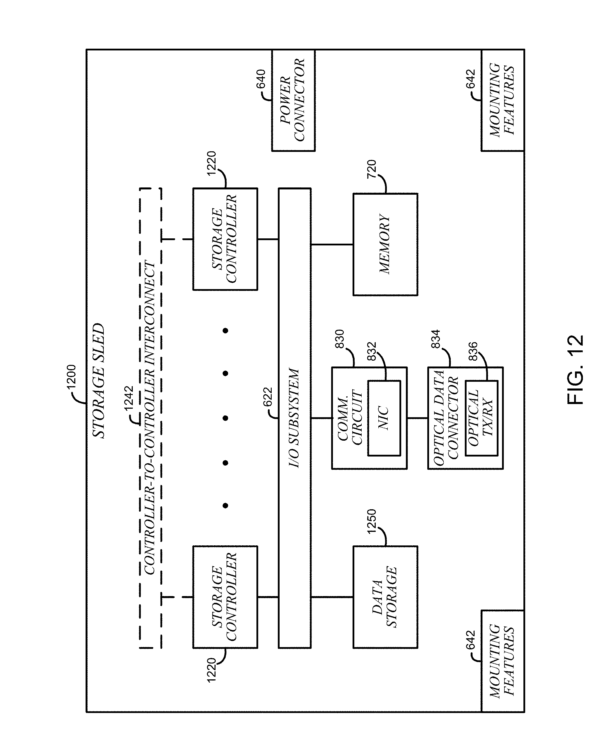
D00013
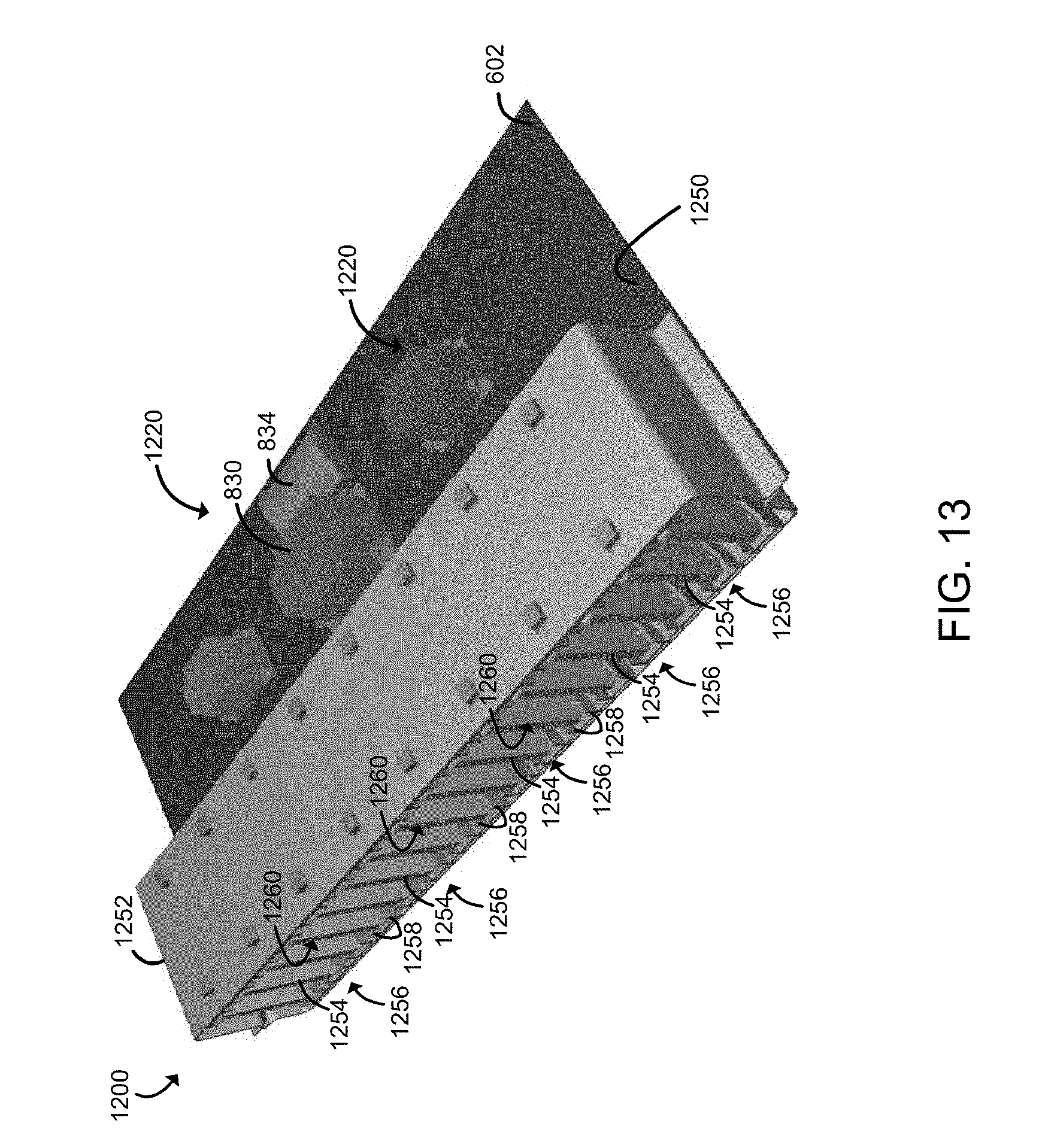
D00014
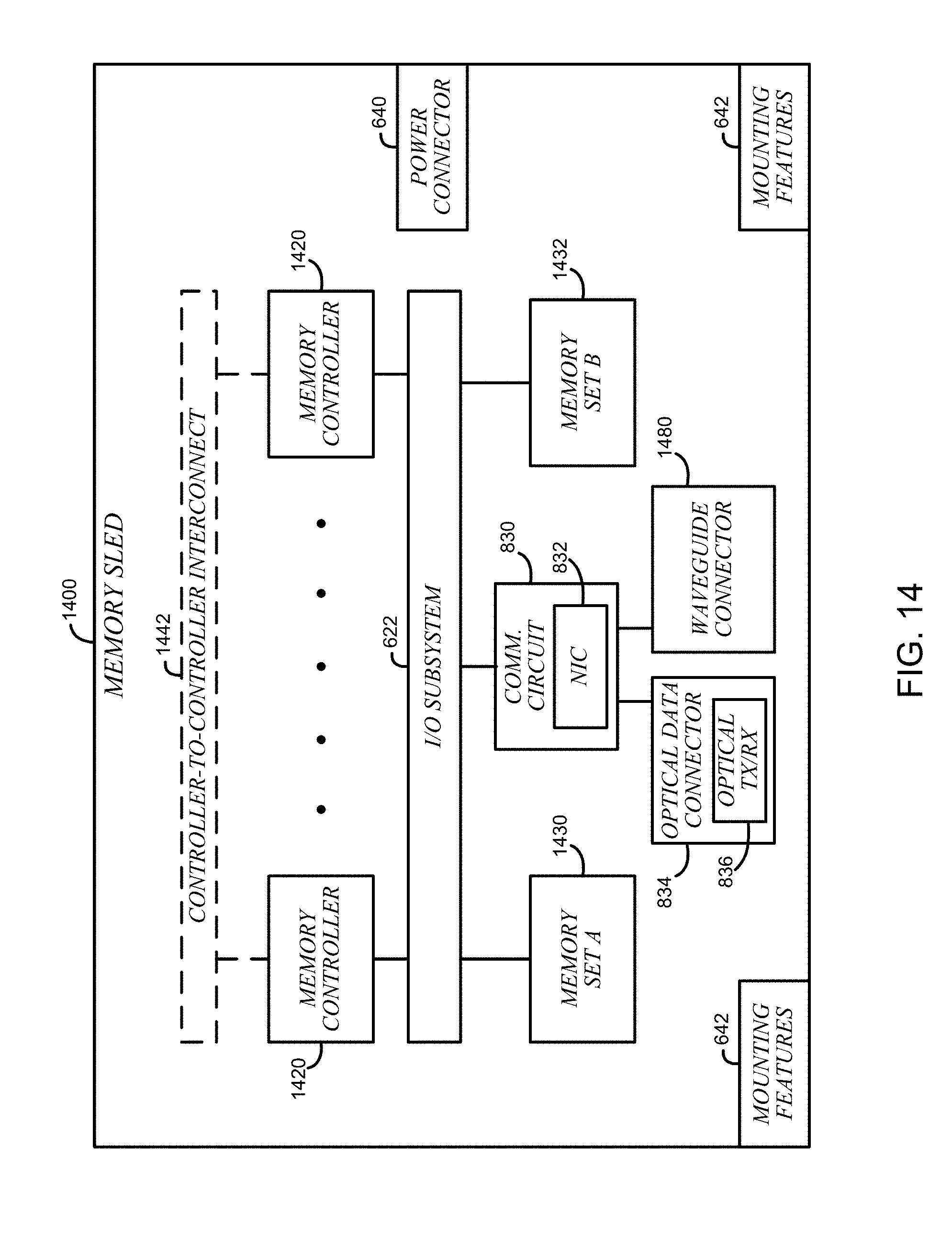
D00015
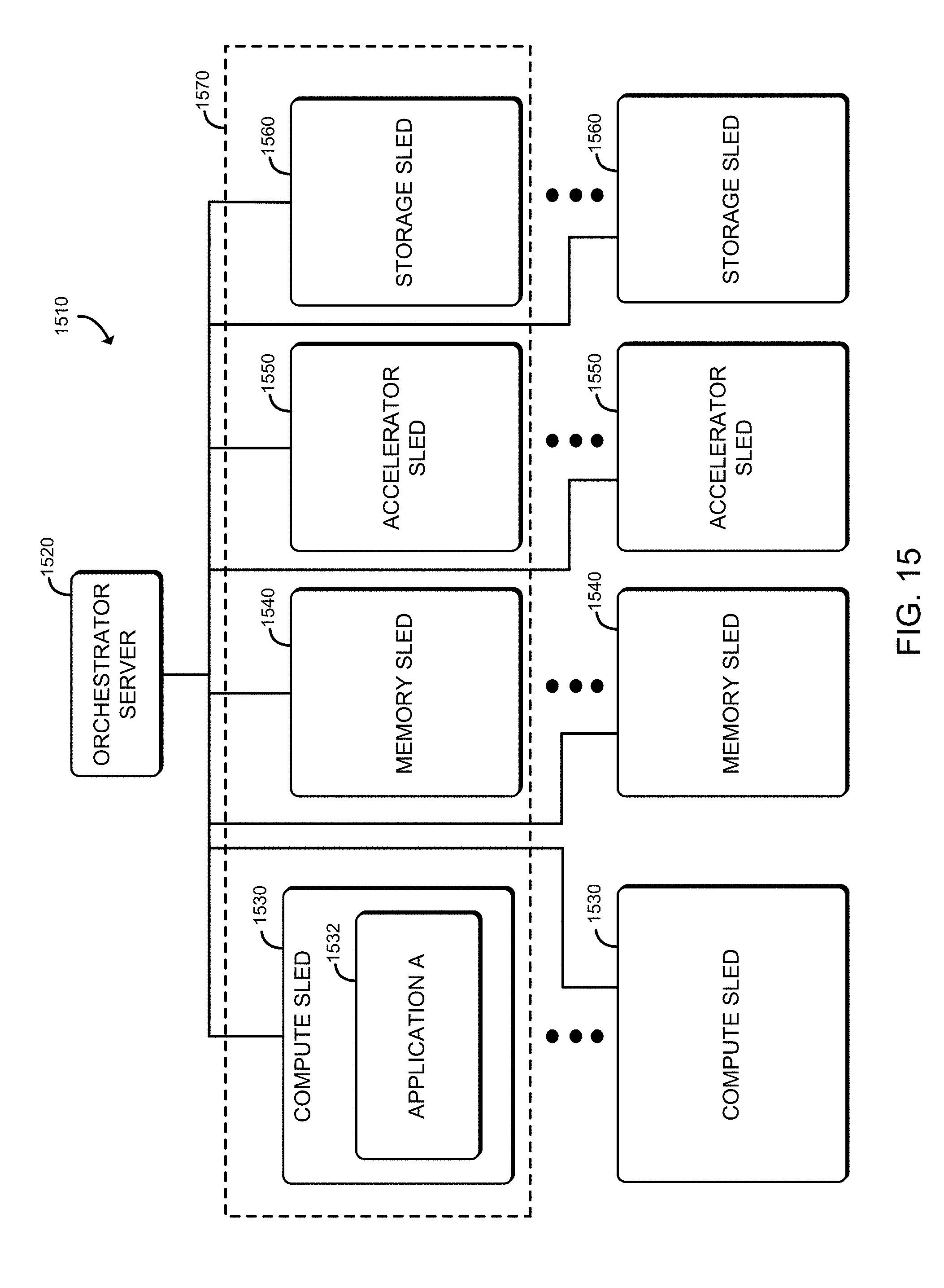
D00016
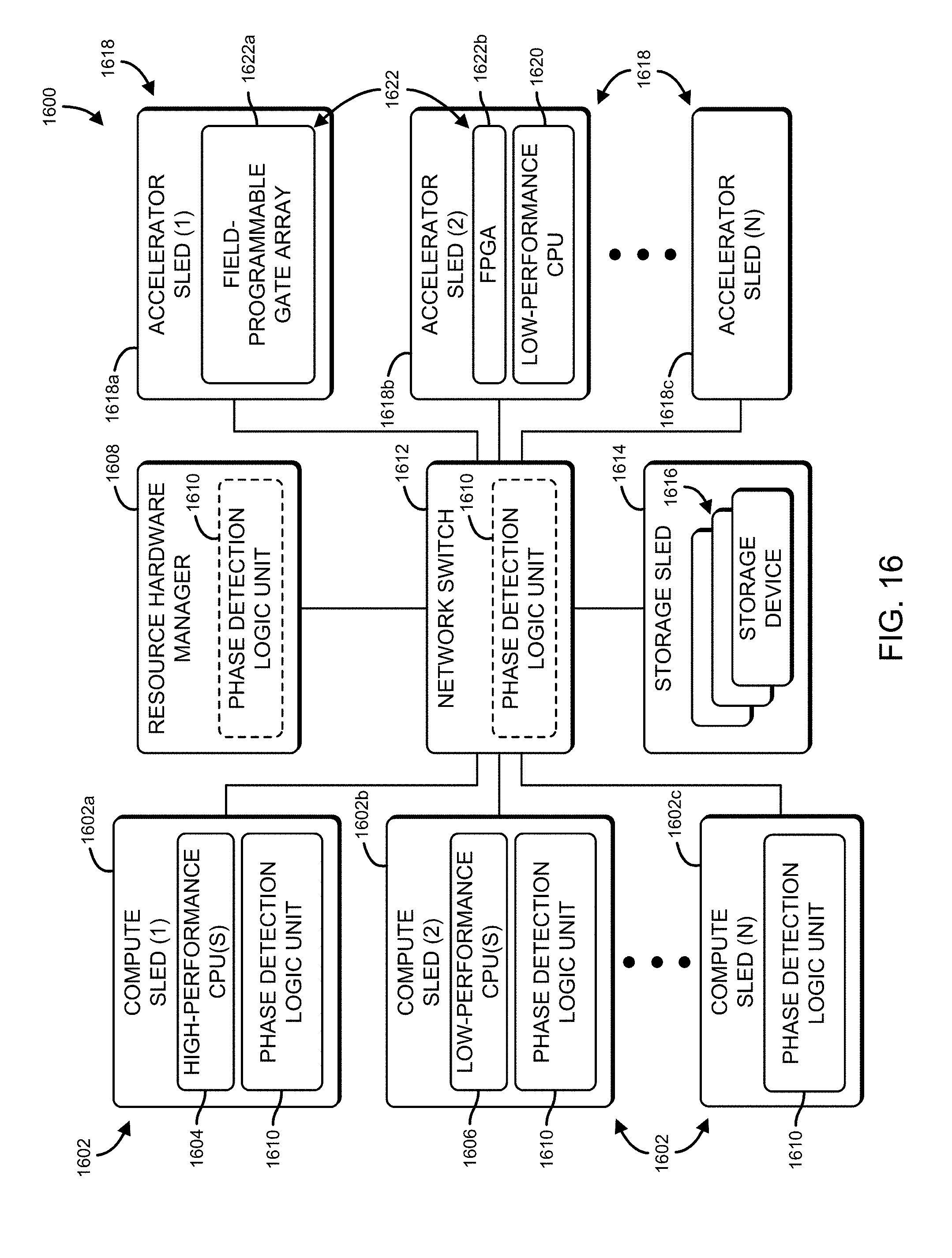
D00017
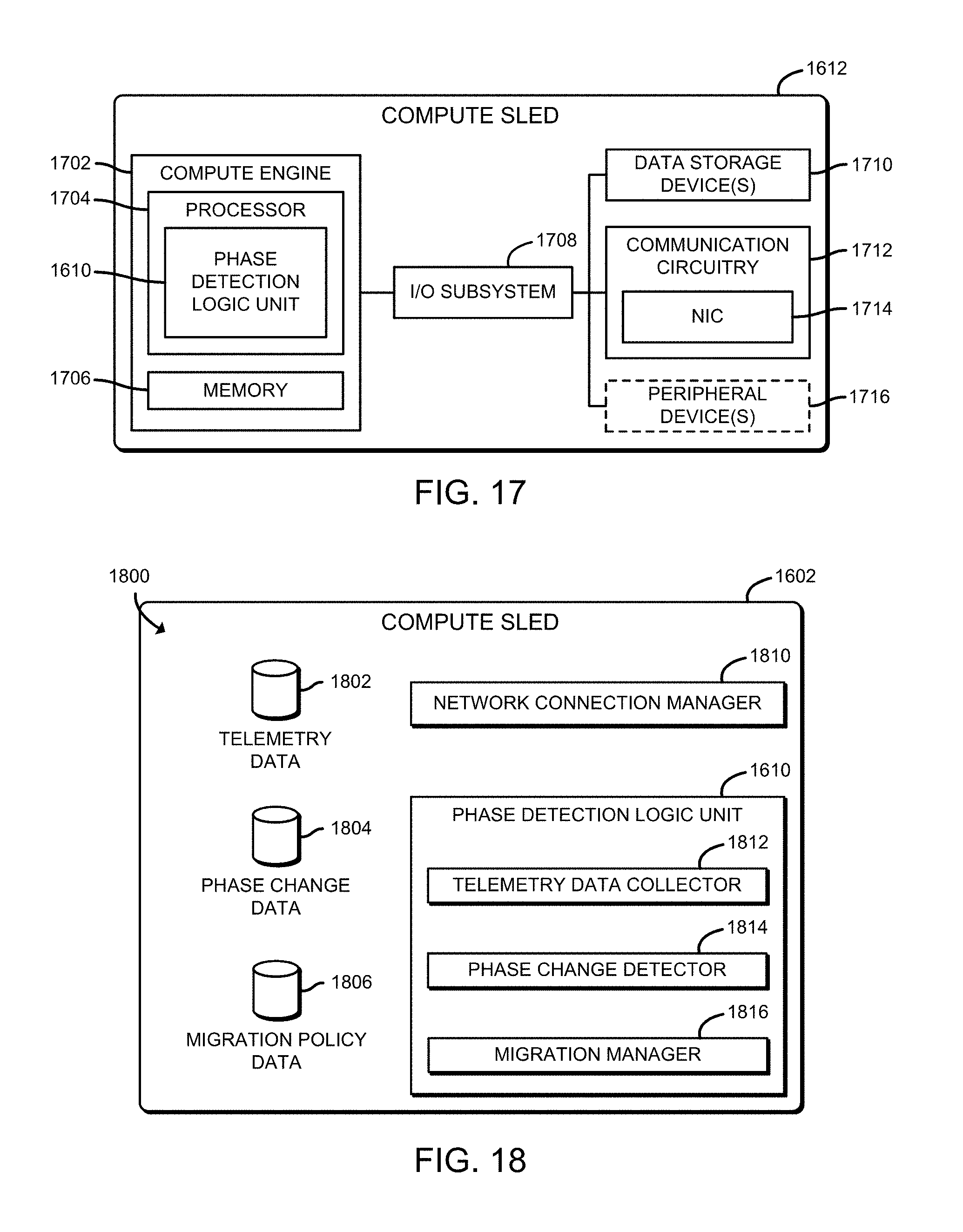
D00018
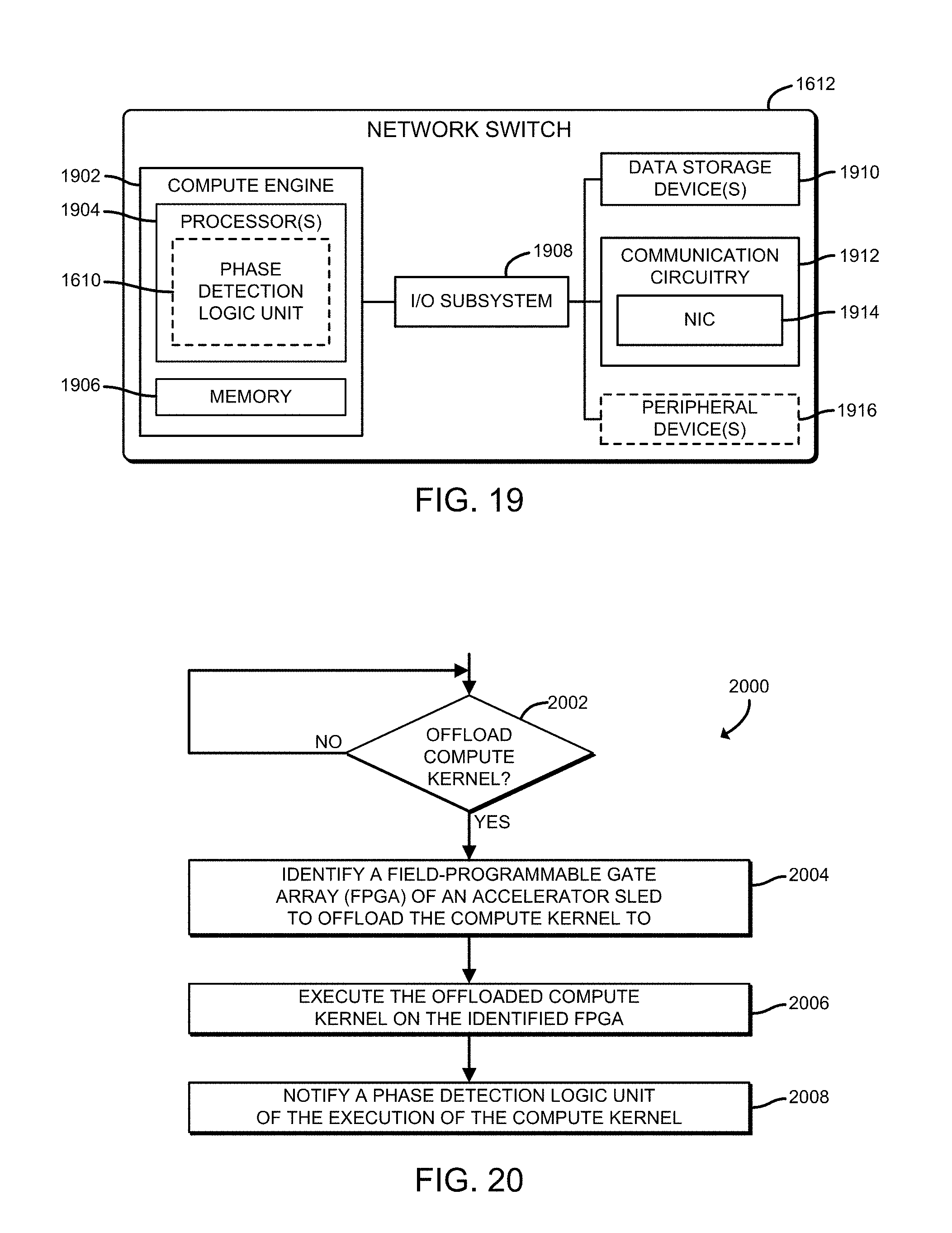
D00019
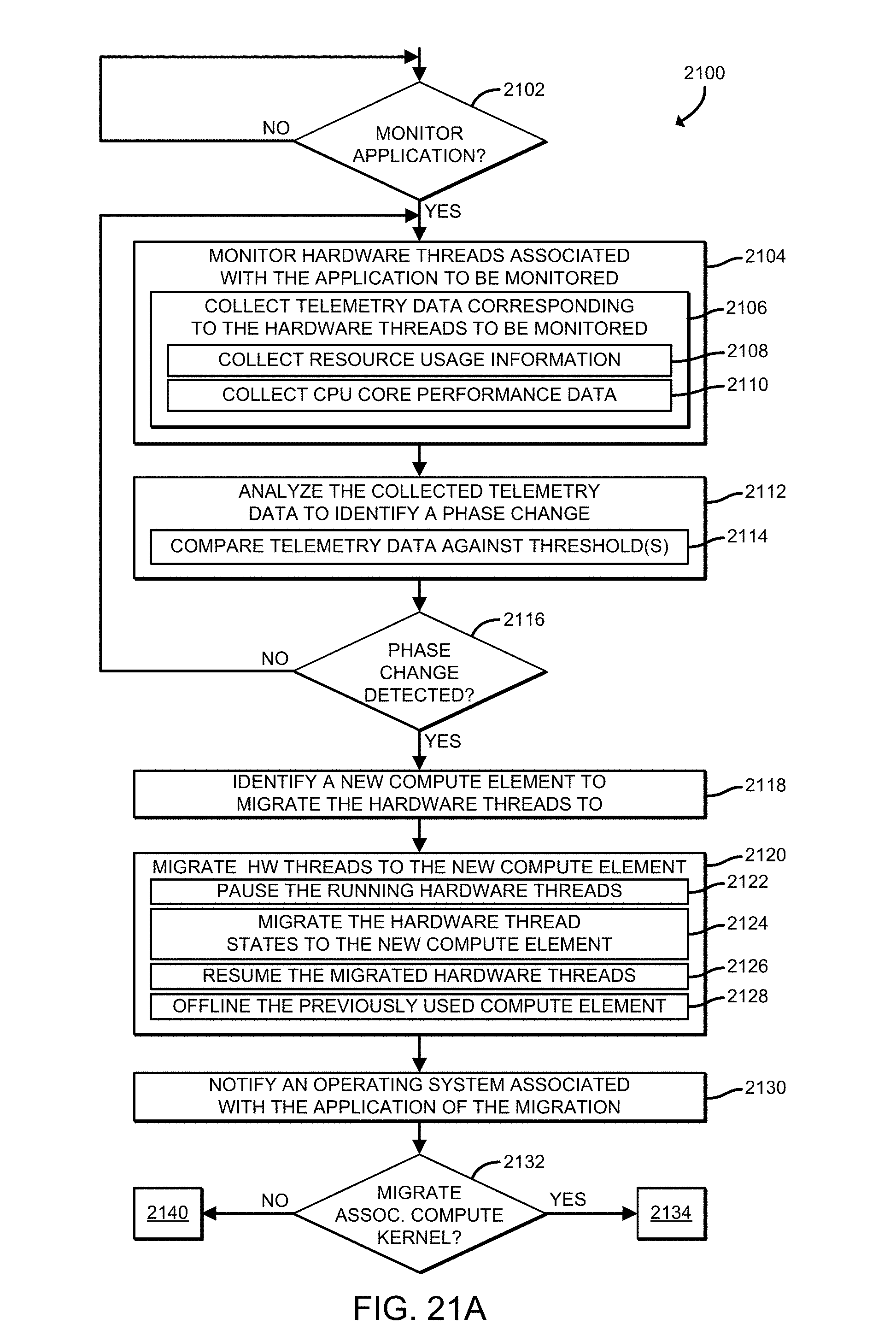
D00020
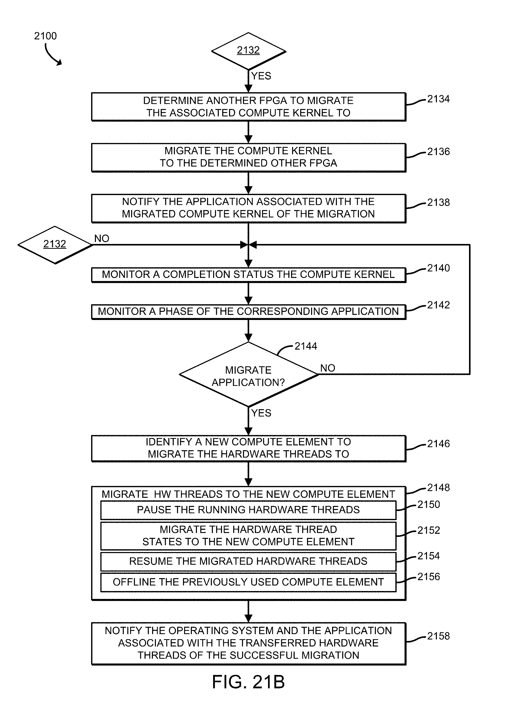
D00021
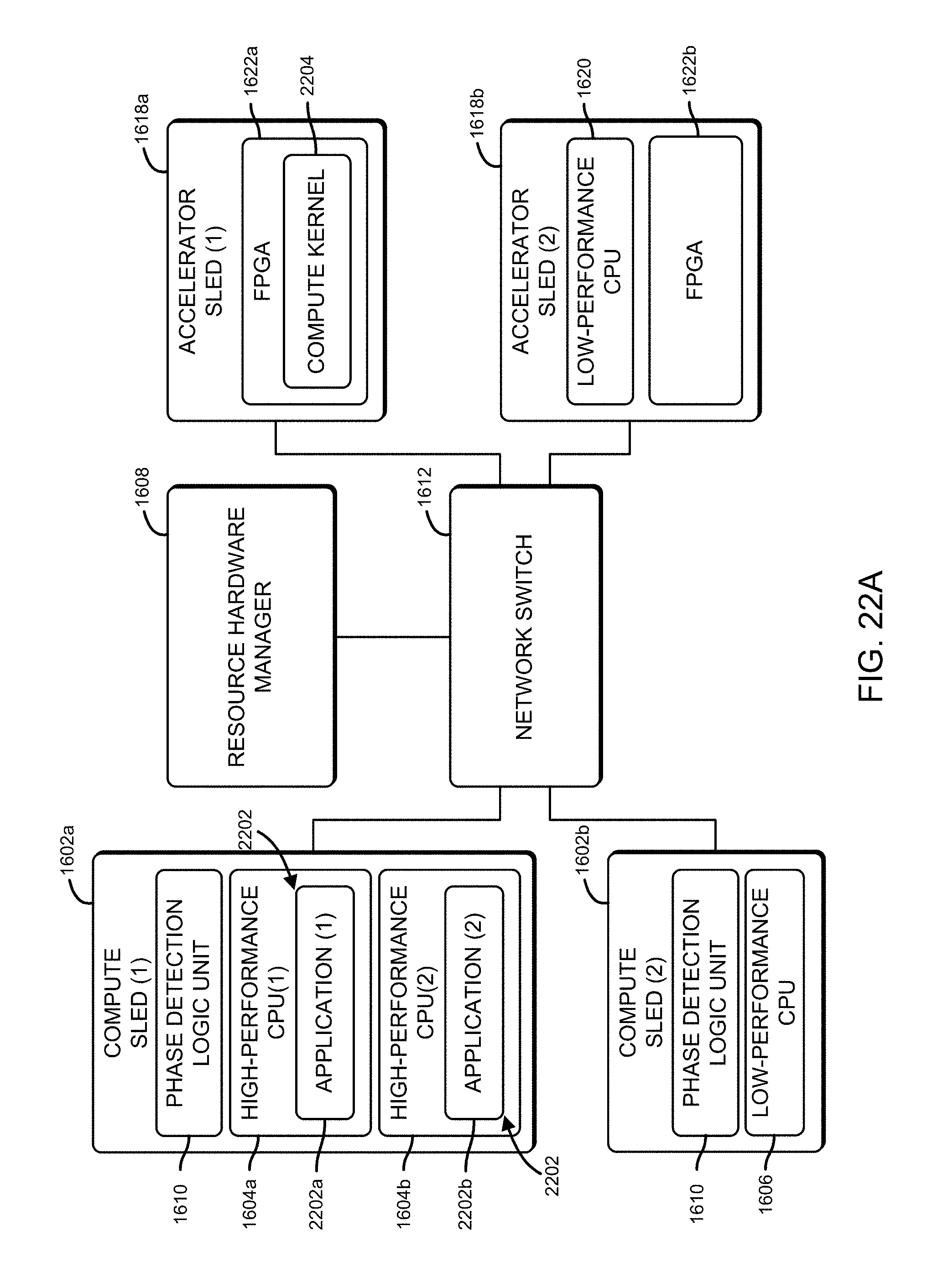
D00022
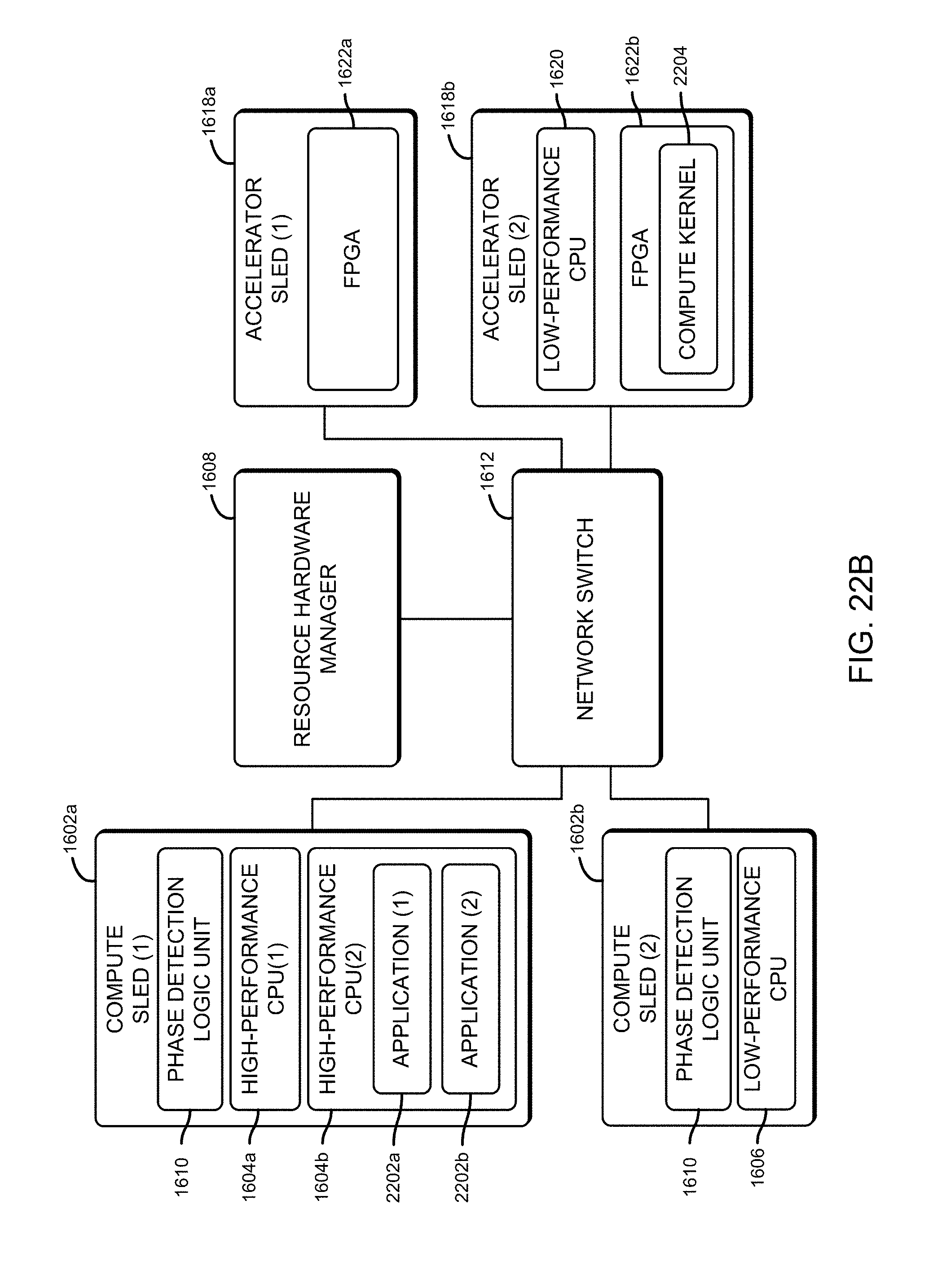
D00023
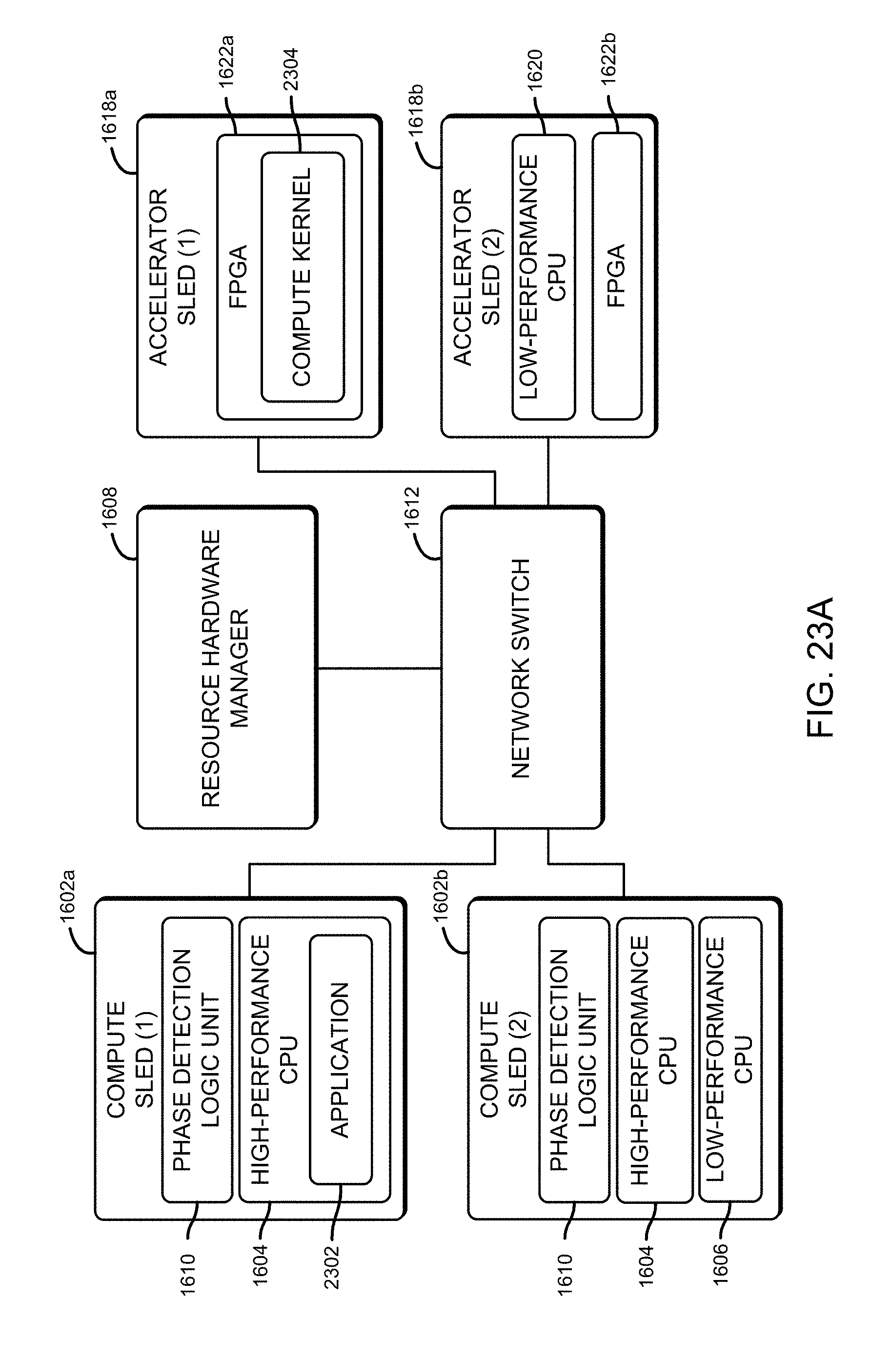
D00024
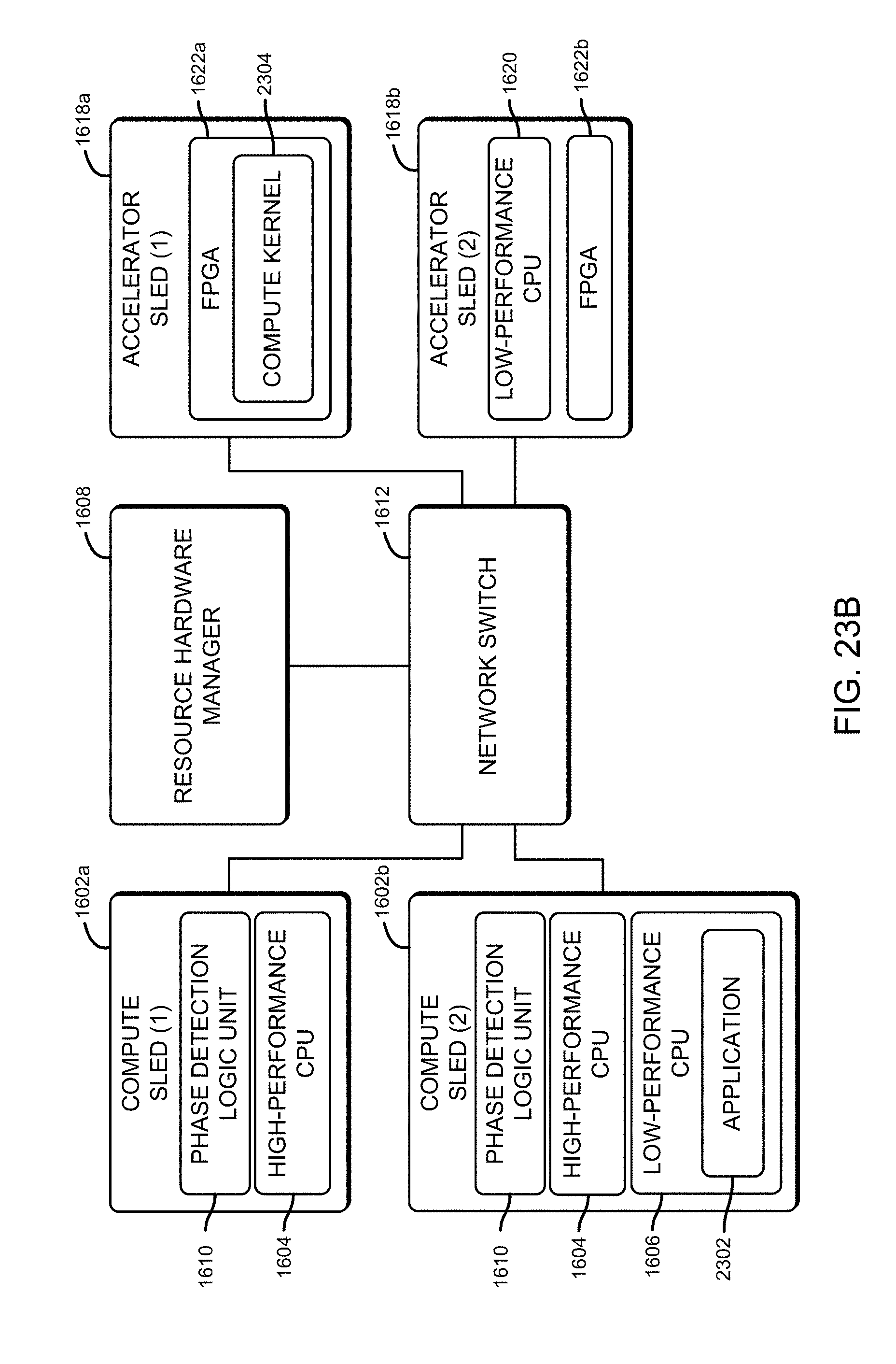
D00025
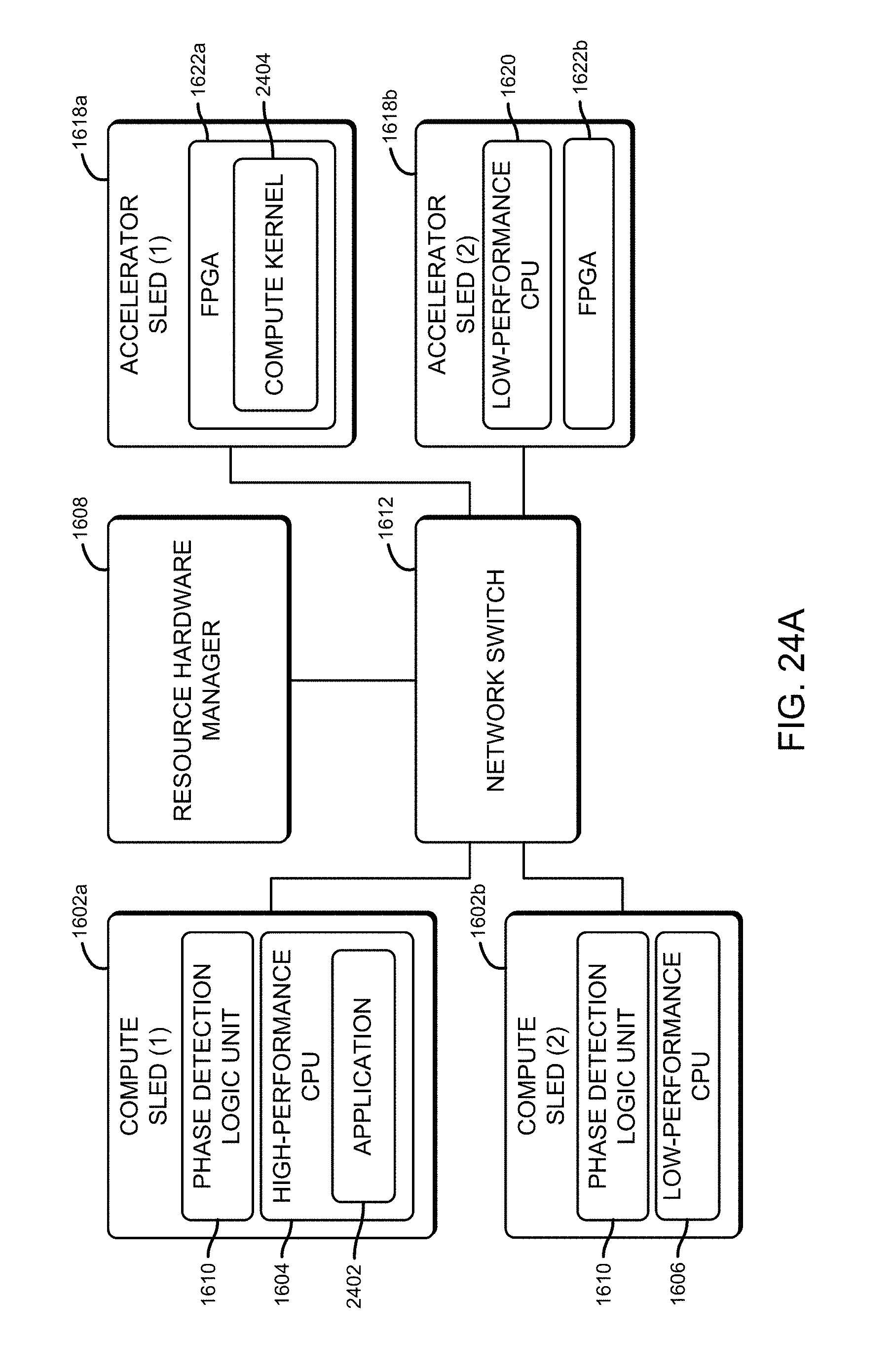
D00026
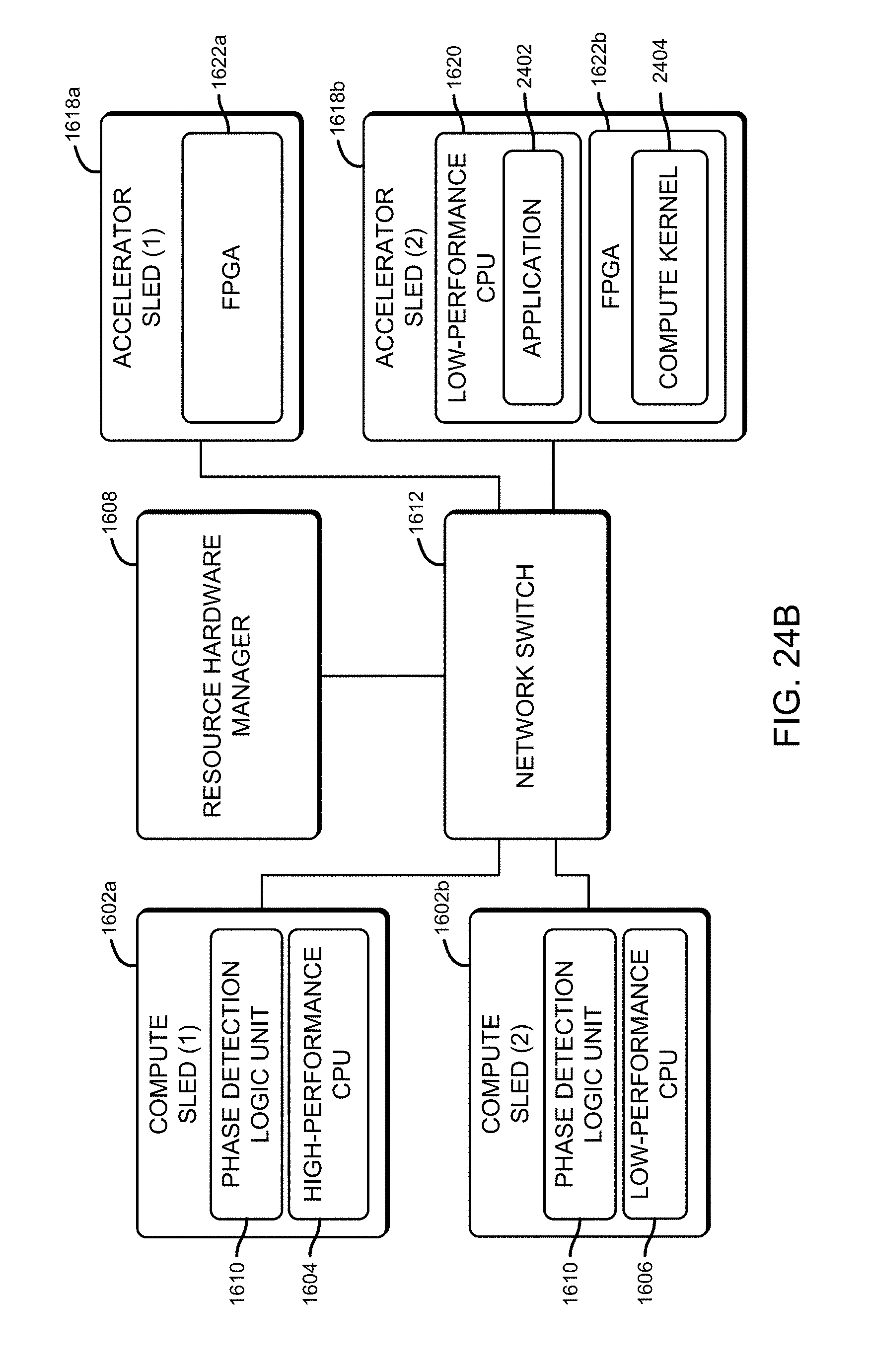
XML
uspto.report is an independent third-party trademark research tool that is not affiliated, endorsed, or sponsored by the United States Patent and Trademark Office (USPTO) or any other governmental organization. The information provided by uspto.report is based on publicly available data at the time of writing and is intended for informational purposes only.
While we strive to provide accurate and up-to-date information, we do not guarantee the accuracy, completeness, reliability, or suitability of the information displayed on this site. The use of this site is at your own risk. Any reliance you place on such information is therefore strictly at your own risk.
All official trademark data, including owner information, should be verified by visiting the official USPTO website at www.uspto.gov. This site is not intended to replace professional legal advice and should not be used as a substitute for consulting with a legal professional who is knowledgeable about trademark law.