Display Device
HYUN; Joobong ; et al.
U.S. patent application number 16/103553 was filed with the patent office on 2019-02-21 for display device. The applicant listed for this patent is LG Display Co., Ltd.. Invention is credited to Kyoseop CHOO, Joobong HYUN, Seungman RYU, Ara YOON.
| Application Number | 20190057238 16/103553 |
| Document ID | / |
| Family ID | 63668180 |
| Filed Date | 2019-02-21 |


| United States Patent Application | 20190057238 |
| Kind Code | A1 |
| HYUN; Joobong ; et al. | February 21, 2019 |
Display Device
Abstract
Disclosed herein is a display device capable of recognizing a fine fingerprint without a complicated construction such as a bulky optical device. The display device comprises a display panel having a display area and a non-display area outside the display area; a light source disposed below the non-display area of the display panel to irradiate the display panel with light; a directional light unit disposed on an upper portion of the display panel, refracting the light supplied from the light source at a first angle to travel from the non-display area to the display area in total internal reflection, reflecting some of the totally internally reflected light at a second angle, and then supplying a light reflected by an object having biometric information to the display panel; and an optical sensor disposed below the display panel and receiving the light exited from the directional light unit.
| Inventors: | HYUN; Joobong; (Paju-si, KR) ; CHOO; Kyoseop; (Paju-si, KR) ; RYU; Seungman; (Paju-si, KR) ; YOON; Ara; (Paju-si, KR) | ||||||||||
| Applicant: |
|
||||||||||
|---|---|---|---|---|---|---|---|---|---|---|---|
| Family ID: | 63668180 | ||||||||||
| Appl. No.: | 16/103553 | ||||||||||
| Filed: | August 14, 2018 |
| Current U.S. Class: | 1/1 |
| Current CPC Class: | G02B 6/4206 20130101; H01L 27/14678 20130101; G06K 9/0004 20130101; G02B 6/4213 20130101 |
| International Class: | G06K 9/00 20060101 G06K009/00; G02B 6/42 20060101 G02B006/42 |
Foreign Application Data
| Date | Code | Application Number |
|---|---|---|
| Aug 16, 2017 | KR | 10-2017-0103812 |
Claims
1. A display device comprising: a display panel having a display area and a non-display area outside the display area; a light source disposed below the non-display area of the display panel to irradiate the display panel with light; a directional light unit disposed on an upper portion of the display panel, and the directional light unit configured to refract the light supplied from the light source at a first angle to travel from the non-display area to the display area in total internal reflection, and reflect some of the totally internally reflected light at a second angle to an object having biometric information, and the directional light unit further configured to supply a light reflected by the object to the display panel; and an optical sensor disposed below the display panel and receiving the light traveling through the directional light unit and the display panel.
2. The display device of claim 1, wherein the directional light unit comprising: a cover substrate disposed to face the display panel to be contacted with the object; an optical element including: a light-exiting element disposed between the cover substrate and the display panel in at least a portion of a region where the light from the light source travels, wherein the at least portion of the region locates at a position corresponding to the display area; and a light-incident element disposed between the cover substrate and the display panel to be overlapped with the light source at a position corresponding to the non-display area; and a first low refractive layer disposed between the optical element and the display panel.
3. The display device of claim 2, wherein the directional light unit further comprises a second low refractive layer disposed between the optical element and the cover substrate.
4. The display device of claim 2, wherein the directional light unit further comprises: an adhesive layer disposed between the optical element and the cover substrate; and a black matrix disposed to overlap the light-incident element and disposed between the cover substrate and the adhesive layer to block some of the light irradiated from the light source.
5. The display device of claim 3, wherein the directional light unit further comprises a black matrix disposed to correspond to the light-incident element and disposed between the cover substrate and the second low refractive layer to block some of the light irradiated from the light source.
6. The display device of claim 3, wherein the directional light unit further comprises: an adhesive layer disposed between the optical element and the second low refractive layer; and a black matrix disposed to overlap the light--incident element between the adhesive layer and the second low refractive layer to block some of the light irradiated from the light source.
7. The display device of claim 4, wherein the light-incident element refracts some of the light incident from the light source at the first angle so as to cause total internal reflection in the cover substrate and make the some of the light travel in the cover substrate, and wherein the light totally internally reflected from an upper surface of the cover substrate and traveling to the light-exiting element is reflected at the second angle smaller than the first angle by the first low refractive layer to be traveled to the cover substrate, and is traveled to the optical sensor after being reflected by the object on the cover substrate.
8. The display device of claim 5, wherein the light-incident element refracts some of the light incident from the light source at the first angle so as to cause total internal reflection in the optical element and make the some of the light travel in the optical element, and wherein the light totally internally reflected from an upper surface of the optical element and traveling to the light-exiting element is reflected at the second angle smaller than the first angle to be traveled to the cover substrate, and is travelled to the optical sensor after being reflected by the object on the cover substrate.
9. The display device of claim 6, wherein the light-incident element refracts some of the light incident from the light source at the first angle so as to cause total internal reflection in the adhesive layer and make the some of the light travel in the adhesive layer, and wherein the light totally internally reflected from an upper surface of the adhesive layer and traveling to the light-exiting element is reflected at the second angle smaller than the first angle to be traveled to the cover substrate, and is travelled to the optical sensor after being reflected by the object on the cover substrate.
10. The display device of claim 7, wherein refractive indexes of the cover substrate, the adhesive layer, and the optical element are the same, and the refractive index of the cover substrate is larger than a refractive index of the first low refractive layer.
11. The display device of claim 8, wherein refractive indexes of the cover substrate and the optical element are the same, a refractive index of the first low refractive layer is the same as that of the second low refractive layer, and a refractive index of the cover substrate is larger than that of the first low refractive layer.
12. The display device of claim 9, wherein refractive indexes of the cover substrate, the adhesive layer and the optical element are the same, a refractive index of the first low refractive layer is the same as that of the second low refractive layer, and a refractive index of the cover substrate is larger than that of the first low refractive layer.
13. The display device of claim 2, wherein the display panel further comprises a polarizing plate disposed between the display panel and the first low refractive layer, and the polarizing plate, the first low refractive layer, and the optical element are substantially similar in size.
14. The display device of claim 2, wherein the display panel further comprises signal lines arranged to bypass a region overlapping the light-incident element of the optical element and the light source.
15. The display device of claim 1, wherein the object includes a fingerprint in which a plurality of ridges and a plurality of valleys are alternately arranged.
Description
CROSS-REFERENCE TO RELATED APPLICATION
[0001] This application claims priority to Republic of Korea Patent Application No. 10-2017-0103812 filed on Aug. 16, 2017 with the Korean Intellectual Property office, which is incorporated herein in its entirety.
BACKGROUND
Field of Technology
[0002] This disclosure relates to a display device, in particular to a display device capable of recognizing a fingerprint using a directional light.
Description of the Related Art
[0003] In recent years, according to development of information communication technology, various information and communication based systems such as notebook computers, tablets, personal computers (PC), smartphones, personal digital assistants (PDA), automated teller machines, and search guidance systems have been developed. As these systems typically store a lot of confidential data such as personal information related to personal privacy as well as business information and trade secret, it is required to enhance security in order to protect the confidential data.
[0004] To do so, one method has been suggested for enhancing the security using an image sensor capable of recognizing a user's biological information. For example, a fingerprint sensor can enhance the security of the systems by registering and authenticating a fingerprint of the user's finger. The fingerprint sensor is for sensing the fingerprint of the user. As the fingerprint sensor, an optical fingerprint sensor has been widely known.
[0005] The optical fingerprint sensor uses a principle of irradiating lights using a light source such as a light emitting diode (LED), and detecting the lights reflected by ridges of the fingerprint using a complementary metal oxide semiconductor (CMOS) image sensor. As the optical fingerprint sensor has to scan the fingerprint using the LED, it is required to equip an additional device for scanning the fingerprint. The additional device increases the size of the optical fingerprint sensor, and thus there are limitations in various applications such as combining with a display device.
[0006] Conventional display devices are configured so that display areas of the display devices can be used as touch areas and fingerprint recognition areas. However, the optical fingerprint sensor uses diffuse light with a significantly lower directionality or directivity as light for recognizing the fingerprint. Therefore, there is a limitation in recognizing patterns of the fingerprint.
[0007] As described above, in the display device having the conventional optical fingerprint sensor, it is difficult to accurately recognize a fingerprint. In order to accurately recognize a fingerprint, a complicated and bulky optical device is required. Accordingly, it is difficult for them to be combined with a portable display device.
SUMMARY
[0008] An object of this disclosure is to provide a display device capable of recognizing a fine fingerprint without a complicated construction such as a bulky optical device.
[0009] Another object of this disclosure is to provide a display device suitable for a display panel with an increased display area and a reduced bezel area.
[0010] A display panel according to this disclosure includes a display panel having a display area and a non-display area outside the display area; a light source disposed below the non-display area of the display panel to irradiate the display panel with light; a directional light unit disposed on an upper portion of the display panel, refracting the light supplied from the light source at a first angle to travel from the non-display area to the display area in total internal reflection, reflecting some of the totally internally reflected light at a second angle, and then supplying a light reflected by an object having biometric information to the display panel; and an optical sensor disposed below the display panel and receiving the light exited from the directional light unit.
[0011] The directional light unit may include a cover substrate disposed to face the display panel to be contacted with the object; an optical element including a light-exiting element disposed between the cover substrate and the display panel in at least a portion of a region where the light from the light source travels at a position corresponding to the display area; and a light-incident element disposed between the cover substrate and the display panel to be overlapped with the light source at a position corresponding to the non-display area; and a first low refractive layer disposed between the optical element and the display panel.
[0012] The directional light unit may further include a second low refractive layer disposed between the optical element and the cover substrate.
[0013] The directional light unit may further include an adhesive layer disposed between the optical element and the cover substrate; and a black matrix disposed to correspond to the optical element between the cover substrate and the adhesive layer to block some of the light irradiated from the light source.
[0014] The directional light unit may further include a black matrix disposed to correspond to the light-incident element between the cover substrate and the second low refractive layer to block some of the light irradiated from the light source.
[0015] The directional light unit may further include an adhesive layer disposed between the optical element and the second low refractive layer; and a black matrix disposed to correspond to the light-incident element between the adhesive layer and the second low refractive layer to block some of the light irradiated from the light source.
[0016] The light-incident element refracts some of the light incident from the light source at a first angle which causes total internal reflection in the cover substrate and progresses it to the cover substrate. The light totally internally reflected from an upper surface of the cover substrate and traveling to the light-exiting element is reflected at a second angle smaller than the first angle by the first low refractive layer to be traveled to the cover substrate, and is traveled to the optical sensor after being reflected by the object on the cover substrate.
[0017] The light-incident element refracts some of the light incident from the light source at a third angle which causes total internal reflection in the optical element and progresses it to the optical element. The light totally internally reflected from an upper surface of the optical element and traveling to the light-exiting element is reflected at a fourth angle smaller than the third angle to be traveled to the cover substrate, and is travelled to the optical sensor after being reflected by the object on the cover substrate.
[0018] The light-incident element refracts some of the light incident from the light source at a fifth angle which causes total internal reflection in the adhesive layer and progresses it to the adhesive layer. The light totally internally reflected from an upper surface of the adhesive layer and traveling to the light-exiting element is reflected at a sixth angle smaller than the fifth angle to be traveled to the cover substrate, and is travelled to the optical sensor after being reflected by the object on the cover substrate.
[0019] Refractive indexes of the cover substrate, the adhesive layer, and the optical element are the same, and the refractive index of the cover substrate is larger than a refractive index of the first low refractive layer.
[0020] Refractive indexes of the cover substrate and the optical element are the same, a refractive index of the first low refractive layer is the same as that of the second low refractive layer, and a refractive index of the cover substrate is larger than that of the first low refractive layer.
[0021] Refractive indexes of the cover substrate, the adhesive layer and the optical element are the same, a refractive index of the first low refractive layer is the same as that of the second low refractive layer, and a refractive index of the cover substrate is larger than that of the first low refractive layer.
[0022] The display panel further comprises a polarizing plate disposed between the display panel and the first low refractive layer, and the polarizing plate, the first low refractive layer, and the optical element have the same size.
[0023] The display panel further comprises signal lines of arranged to bypass a region overlapping the light-incident element of the optical element and the light source.
[0024] The object includes a fingerprint in which a plurality of ridges and a plurality of valleys are alternately arranged
[0025] In the display device according to this disclosure described above, it is possible to reconstruct an image sensed using a directional light unit and an optical sensor. Therefore, it is possible to correctly recognize a fine fingerprint without a complicated structure such as a bulky optical apparatus.
[0026] In addition, it is possible to easily adapt to a display panel having a reduced bezel area (non-display area) since a light-incident element of optical element and a light source are disposed on the non-display portion of the display panel.
BRIEF DESCRIPTION OF THE DRAWINGS
[0027] The accompanying drawings, which are included to provide a further understanding of the invention and are incorporated in and constitute a part of this specification, illustrate embodiments of the invention and together with the description serve to explain the principles of the invention. In the drawings:
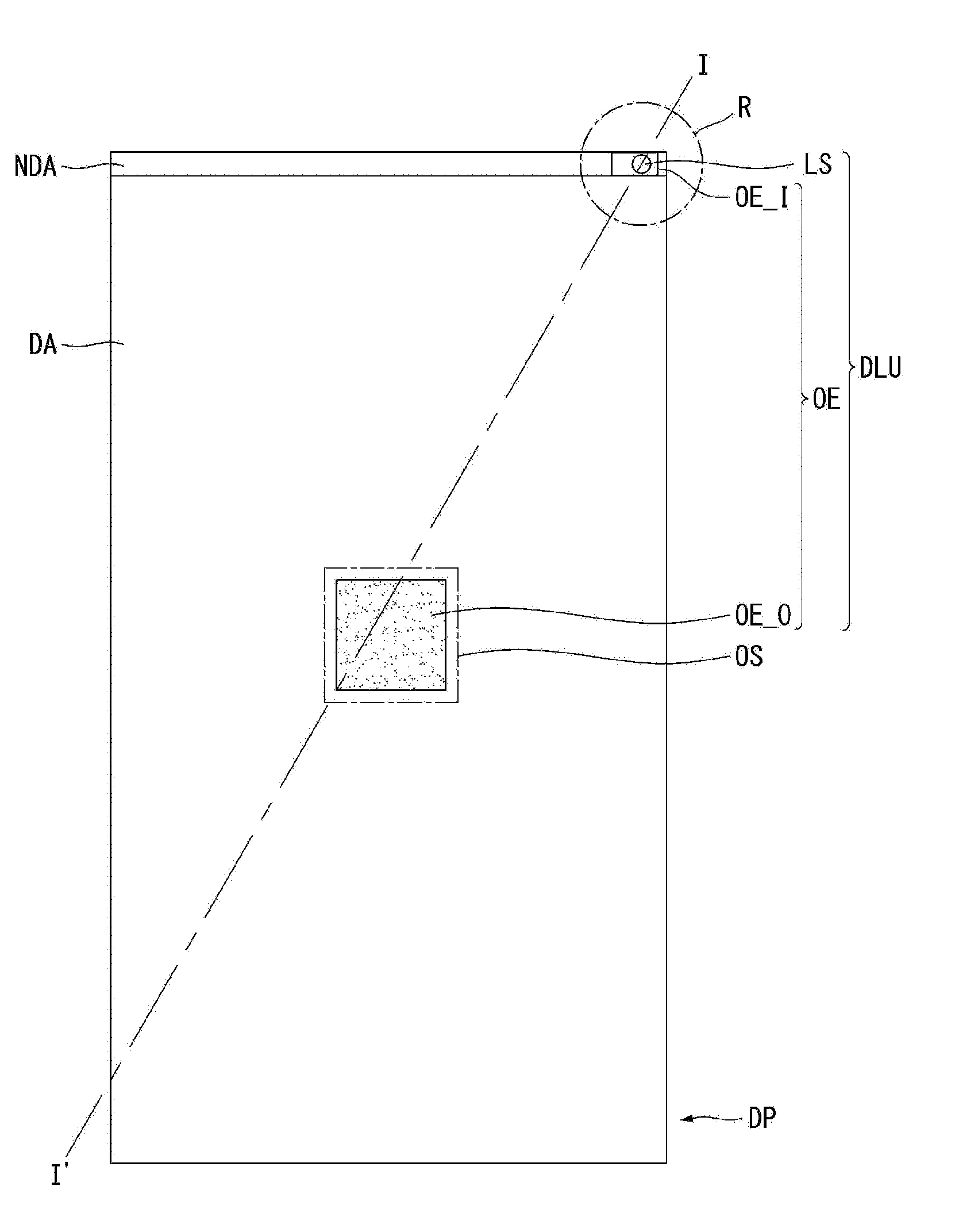
[0028] FIG. 1A is a planar view illustrating a display device according to an embodiment of this disclosure;
[0029] FIG. 1B is an enlarged planar view for illustrating a region R shown in FIG. 1A according to an embodiment of this disclosure;
[0030] FIG. 2 is a planar view illustrating an optical element included in a directional light unit of the display device shown in FIG. 1A according to an embodiment of this disclosure;
[0031] FIG. 3A is a cross-sectional view illustrating a display device according to a first embodiment of this disclosure taken along a line I-I' shown in FIG. 1A, and showing a light path traveling through a total internal reflection in the directional light unit according to an embodiment of this disclosure;
[0032] FIG. 3B is a cross-sectional view illustrating a display device according to the first embodiment of this disclosure taken along a line I-I' shown in FIG. 1A, and showing a light path in which the light refracted by a light-exiting element of the optical element is converged on an optical sensor according to an embodiment of this disclosure;
[0033] FIG. 4A is a cross-sectional view illustrating a display device according to a second embodiment of this disclosure taken along a line I-I' shown in FIG. 1A according to an embodiment of this disclosure, and showing a light path traveling through a total internal reflection in the directional light unit;
[0034] FIG. 4B is a cross-sectional view illustrating a display device according to the second embodiment of this disclosure taken along a line I-I' shown in FIG. 1A, and showing a light path in which the light refracted by a light-exiting element of the optical element is converged on an optical sensor according to an embodiment of this disclosure;
[0035] FIG. 5A is a cross-sectional view illustrating a display device according to a third embodiment of this disclosure taken along a line I-I' shown in FIG. 1A, and showing a light path traveling through a total internal reflection in the directional light unit according to an embodiment of this disclosure; and
[0036] FIG. 5B is a cross-sectional view illustrating a display device according to the third embodiment of this disclosure taken along a line I-I' shown in FIG. 1A, and showing a light path in which the light refracted by a light-exiting element of the optical element is converged on an optical sensor according to an embodiment of this disclosure.
DETAILED DESCRIPTION
[0037] Hereinafter, embodiments of this disclosure are described in detail with reference to the accompanying drawings. In the specification, the same reference numerals denote the same elements. In the following description, a detailed description of the known functions and constitutions will be omitted if it is deemed to obscure the embodiments of the present invention. Furthermore, the names of elements used in the following description have been selected by taking into consideration only the ease of writing this specification and may be different from the names of actual parts. Also, as an example of the touch sensor integrated type display device, a touch sensor integrated type liquid crystal display device will be described in detail.
[0038] A display device according to an embodiment of this disclosure is described below with reference to FIGS. 1A and 1B.
[0039] FIG. 1A is a planar view illustrating a display device according to an embodiment of this disclosure, and FIG. 1B is an enlarged planar view for illustrating a region R shown in FIG. 1A.
[0040] Referring to FIGS. 1A and 1B, the display device according to the embodiment of this disclosure includes a display panel DP having a display area DA and a non-display area NDA, a directional light unit DLU coupled with the display panel DP, and an optical sensor OS.
[0041] As the display panel DP, any display panel may be used as long as the non-display area NDA can transmit light. In typical, a display panel of an electroluminescent display device using a flexible translucent substrate may be used. A plurality of signal lines SL for supplying various control signals and data signals to display elements of the display area DA may be disposed in the non-display area NDA of the display panel DP. It is preferable that the plurality of signal lines SL are disposed to avoid a light source LS of the directional light unit DLU and a light-incident element OE_I of an optical element OE so as not to obstruct a path of the light supplied from the light source LS.
[0042] The directional light unit DLU may include the light source LS, the optical element OE, and a cover substrate (not shown).
[0043] The light source LS is disposed below the non-display area NDA of the display panel DP to irradiate the display panel DP with light. It is preferable to use a light source that supplies a collimated light capable of providing a light having a high collimation, such as an infrared laser.
[0044] The optical element OE refracts the light supplied from the light source LS at a first angle to travel the light from the non-display area NDA to the display area DA in a total internal reflection, and then reflects some of the totally internally reflected light at a second angle smaller than the first angle. And then, the optical element OE supplies the light reflected by an object having biometric information to the display panel DP.
[0045] The optical element OE includes a light-incident element OE_I and the light-exiting element OE_O separated from each other at a predetermined distance. The light-incident element OE_I and the light-exiting element OE_O are transparent holographic recording films, and the refractive index of each of the light-incident element OE_I and the light-exiting element OE_O may be the same as or slightly larger than that of a cover substrate.
[0046] The light-incident element OE_I converts the light supplied from the light source LS into a progressing light. The progressing light is converted to have a constant diffusion angle e in a horizontal plane consisting of a longitudinal axis and a widthwise axis. Also, the progressing light maintains its original collimated state in a vertical plane consisting of the longitudinal axis and a thickness direction axis. The diffusion angle .theta. may be set to be equal to or larger than an inner angle formed by two line segments connecting an incident point at which light is incident and the two end points of the other side of the cover substrate shown in FIG. 2. The progressing light advances while spreading in a triangular shape having the diffusion angle .theta.. The triangular area occupied by the diffusion of the progressing light becomes an image recognition area ISA.
[0047] If no object is present on a surface of the cover substrate, the progressing light 100 may be totally internally reflected in the cover substrate to travel inside the cover substrate. However, if there is an object on the surface of the cover substrate, some of the progressing light 100 are refracted by the object and is exited to the outside of the cover substrate CS. For example, if an object having biometric information is brought into contact with the image recognition area ISA of the cover substrate CS, some of the light is reflected or absorbed by the object, and some of the light is reflected and propagated inside the cover substrate.
[0048] Specifically, the object having biometric information may include a finger having a fingerprint in which a plurality of ridges and a plurality of valleys are alternately arranged. If the object is a finger, the progressing light travelling to the ridge portion of the fingerprint of the finger is absorbed by the ridge of the fingerprint and is exited to the outside of the cover substrate. On the other hand, the progressing light travelling to the valley portion of the fingerprint is reflected in the cover substrate and proceeds.
[0049] The light-exiting element OE_O exits some of the progressing light 100 travelling inside the cover substrate to the display panel DP. If an object having an image (for example, a human finger having a fingerprint) is touched on the upper surface of the cover substrate CS, the light-exiting element OE_O makes some of the light refracted by the finger to be supplied to the display panel DP.
[0050] The cover substrate may include a predetermined area capable of recognizing the object having biometric information. The predetermined area may be taken from a portion area of the image sensing area as shown in FIG. 2. The cover substrate CS can be made of transparent reinforced glass with a refractive index of about 1.5.
[0051] The optical sensor OS receives the light exited through the optical element OE and supplies the light to a host system (not shown).
[0052] On the other hand, the directional light unit DLU may further include a low refractive layer or the like. The specific configuration of the directional light unit DLU will be described later in detail with reference to FIGS. 3A to 5B.
[0053] In the display device according to this disclosure described above, it is possible to reconstruct an image sensed using the directional light unit DLU and the optical sensor OS. Therefore, it is possible to correctly recognize a fine fingerprint without a complicated structure such as a bulky optical apparatus.
[0054] A display device according to a first embodiment of this disclosure is described below with reference to FIGS. 3A and 3B.
[0055] FIG. 3A is a cross-sectional view illustrating a display device according to a first embodiment of this disclosure taken along a line I-I' shown in FIG. 1A, and showing a light path traveling through a total internal reflection in the directional light unit. FIG. 3B is a cross-sectional view illustrating a display device according to the first embodiment of this disclosure taken along a line I-I' shown in FIG. 1A, and showing a light path in which the light refracted by a light-exiting element of the optical element is converged on an optical sensor.
[0056] Referring to FIGS. 3A and 3B, the display device according to the first embodiment of this disclosure includes a display panel DP having a display area DA and a non-display area NDA, a light source LS disposed to correspond to the non-display area NDA, a directional light unit coupled with the display panel DP to progress and exit the light from the light source LS, and an optical sensor OS which senses or detects the light from the directional light unit DLU.
[0057] As the display panel DP, any display panel may be used as long as the non-display area NDA can transmit light. In typical, a display panel of an electroluminescent display device using a flexible translucent substrate may be used. However, this disclosure is not limited thereto. A liquid crystal display (LCD), a plasma display panel (PDP), a field emission display (FED) or the like may be used in this disclosure if their non-display areas can transmit light. A polarizing plate POL may be attached to an upper side of the display panel DP to improve visibility.
[0058] The light source LS is disposed below the non-display area NDA of the display panel DP to irradiate the display panel DP with light. The light source LS may be a light source that supplies a collimated light capable of providing a light having a high collimation, such as an infrared laser in one embodiment.
[0059] The directional light unit may include a cover substrate CS, a low refractive layer LR and the light source LS. The directional light unit refracts the light supplied from the light source LS to progress it from the non-display area NDA to the display area DA in a total internal reflection, reflects some of the totally internally reflected light, and supplies the light reflected by the object having biometric information to the display panel DP and the optical sensor OS.
[0060] The cover substrate CS may include a predetermined area capable of recognizing the object having biometric information. The cover substrate CS can be made of transparent reinforced glass with a refractive index of about 1.5. A black matrix BM may be attached to the edge of the cover substrate CS to correspond to the light source LS. The object having biometric information may include a finger having a fingerprint F in which a plurality of valleys V and a plurality of ridges R are alternately arranged.
[0061] The low refraction layer LR is disposed between the cover substrate CS and the display panel DP. It is preferable that the low refraction layer LR has a refractive index lower than that of the cover substrate CS. The refractive index of the low refractive layer LR is preferably similar to the refractive index of the object to be recognized. For example, if the display device of this disclosure is applied to fingerprint recognition, the low refractive layer LR may have a refractive index of about 1.4 similar to the refractive index of human skin of 1.39.
[0062] The optical element OE is disposed between the cover substrate CS and the low refractive layer LR and may include the light-incident element OE_I and the light-exiting element OE_O. The light-incident element OE_I and the light-exiting element OE_O are transparent holographic recording films. The refractive index of the light-incident element OE_I and the light-exiting element OE_O may be the same as or slightly larger than that of the cover substrate CS.
[0063] The light-incident element OE_I is disposed to correspond to the non-display area NDA, and is arranged so as to overlap the black matrix BM and the light source LS. The light-incident element OE_I refracts some of the light incident from the light source LS at a first angle 01 which causes total internal reflection in the cover substrate CS, and progresses it to the cover substrate CS. Since the progressing light has already been described with reference to FIG. 2, further explanation is omitted.
[0064] The light-exiting element OE_O may be disposed in at least a portion of area where light from the light source LS travels at a position corresponding to at least a portion of the image recognition area ISA defined by the progressing light. In this case, the light-exiting element OE_O may be disposed at a predetermined distance from the light-incident element OE_I. The light-exiting element OE_O reflects the incident light at a second angle .theta.2 smaller than the first angle .theta.1 and exits the reflected light to the cover substrate CS. The light is reflected by the object and is progressed to the display panel DP and an optical sensor OS.
[0065] The optical sensor OS is disposed outside the display panel DP at a position corresponding to the light-exiting element OE_O of the optical element OE. The optical sensor OS senses the amount of light transmitted through the display panel DP.
[0066] An adhesive layer AD may be further disposed between the cover substrate CS and the optical element OE. The adhesive layer AD is for coupling the cover substrate CS with the optical element OE. The refractive index of the adhesive layer AD may be substantially the same as that of the cover substrate CS.
[0067] In the embodiment of FIGS. 3A and 3B, it is possible to integrate the polarizing plate POL, the low refractive layer LR and the optical element OE in only one process because they have substantially a same size.
[0068] Next, referring to FIGS. 3A and 3B, there will be described about a case in which light emitted from the light source is converted into the progressing light by the optical element to travel in the display area, and a case in which after the progressing light is reflected by the object, the reflected light is converged to the optical sensor to sense an image of the object.
[0069] Referring to FIG. 3A, the light emitted from the light source LS is transmitted through the display panel DP, the polarizing plate POL and the low refractive layer LR, and incident to the light-incident element OE_I of the optical element OE. The light-incident element OE_I refracts the incident light at a first angle .theta.1 to cause total internal reflection in the cover substrate CS. Some of the light that has passed through the light-incident element OE_I travels to the black matrix BM, and the remaining of the light is refracted at the first angle .theta.1 to travel from the non-display area NDA to the display area DA. Accordingly, it is possible prevent the light from leaking in the non-display area NDA because the light arrived at the black matrix BM is blocked by the black matrix BM. The adhesive layer AD and the cover substrate CS disposed on the optical element OE and the cover substrate CS have substantially the same refractive index so that the light refracted from the light-incident element OE_I and then advancing in the display area DA is arrived at the upper surface of the cover substrate CS, and is totally internally reflected. The totally internally reflected light is transmitted through the cover substrate CS and the adhesive layer AD and is totally internally reflected again on the lower surface of the optical element OE. That is, since the refractive index of the optical element OE is substantially similar to that of the cover substrate and the adhesive layer, and the refractive index of the low refractive layer LR disposed under the optical element OE is smaller than that of the cover substrate, the light totally internally reflected at the upper surface of the cover substrate CS does not transmit the low refractive layer LR but is totally internally reflected by the low refractive layer LR, thereby traveling back to the cover substrate CS. Like this, some of the light emitted from the light source LS and refracted by the light-incident element OE_I is reflected by total internal reflection between the upper surface of the cover substrate CS and the lower surface of the optical element OE, thereby traveling to the area corresponding to the display area DA as shown in FIG. 3A. In FIG. 3A, in case that an object (for example, a finger) having a fingerprint F with biometric information is touched on the upper surface of the cover substrate CS, the light is absorbed when it meets the ridge R of the fingerprint F, but the light is reflected when it meets the valley V of the fingerprint F. Accordingly, the light traveling to the top surface of the cover substrate CS keeps a total-reflection state and progresses in the display area DA.
[0070] Referring to FIG. 3B, some of the light totally internally reflected at the upper surface of the cover substrate CS reaches to the light-exiting element OEO. The light scattered by patterns of the light-exiting element OE_O among the light reached the light-exiting element OE_O, reflected at a second angle .theta.2 smaller than the first angle .theta.1, and maintaining the total-reflection, is advanced into the cover substrate CS via the adhesive layer AD. At this time, when the finger is touched on the cover substrate CS, the light reached to the ridge R of the fingerprint F is absorbed, and the light reached to the valley V of the fingerprint F is reflected to transmit the adhesive layer AD, the optical element OE, the low refractive layer LR, the polarizing plate POL, and the display panel DP. The optical sensor OS located below the display panel DP senses the amount of light reflected by the ridge R and the valley V of the fingerprint F. The light sensed by the optical sensor OS can be used to reconstruct the fingerprint pattern of the finger after being supplied to an image sensing IC (not shown) through lead-out lines.
[0071] In the display device according to the embodiment of FIGS. 3A and 3B of this disclosure, it is possible to reconstruct an image sensed using the directional light unit and the optical sensor. Therefore, it is possible to correctly recognize a fine fingerprint without a complicated structure such as a bulky optical apparatus.
[0072] In addition, it is possible to easily adapt to a display panel having a reduced bezel area since a light-incident element of an optical element and a light source are disposed on the non-display portion of the display panel.
[0073] Hereafter, a display device according to a second embodiment of this disclosure is described with reference to FIGS. 4A and 4B.
[0074] FIG. 4A is a cross-sectional view illustrating a display device according to a second embodiment of this disclosure taken along a line I-I' shown in FIG. 1A, and showing a light path traveling through a total internal reflection in the directional light unit. FIG. 4B is a cross-sectional view illustrating a display device according to the second embodiment of this disclosure taken along a line I-I' shown in FIG. 1A, and showing a light path in which the light refracted by a light-exiting element of the optical element is converged on an optical sensor.
[0075] Referring to FIGS. 4A and 4B, the display device according to the second embodiment of this disclosure includes a display panel DP having a display area DA and a non-display area NDA, a light source LS disposed to correspond to the non-display area NDA, a directional light unit coupled with the display panel DP to progress and exit the light from the light source LS, and an optical sensor OS senses or detects the light from the directional light unit DLU.
[0076] As the display panel DP, any display panel may be used as long as the non-display area NDA can transmit light. In typical, a display panel of an electroluminescent display device using a flexible translucent substrate may be used. However, this disclosure is not limited thereto. A liquid crystal display (LCD), a plasma display panel (PDP), a field emission display (FED) or the like may be used in this disclosure if their non-display areas can transmit light. A polarizing plate POL may be attached to an upper side of the display panel DP to improve visibility.
[0077] The light source LS is disposed below the non-display area NDA of the display panel DP to irradiate the display panel DP with light. It is preferable to use a light source that supplies a collimated light capable of providing a light having a high collimation, such as an infrared laser.
[0078] The directional light unit may include a first low refractive layer LR1, an optical element OE, a second low refractive layer LR2 and a cover substrate CS. The directional light unit refracts the light supplied from the light source LS to progress it from the non-display area NDA to the display area DA in a total internal reflection, reflects some of the totally internally reflected light, and supplies the light reflected by an object having biometric information to the display panel DP and the optical sensor OS.
[0079] The cover substrate CS may include a predetermined area capable of recognizing the object having biometric information. The cover substrate CS can be made of transparent reinforced glass with a refractive index of about 1.5. A black matrix BM may be attached to the edge of the cover substrate CS to correspond to the light source LS. The object having biometric information may include a finger having a fingerprint F in which a plurality of valleys V and a plurality of ridges R are alternately arranged.
[0080] The first low refraction layer LR1 is disposed between the cover substrate CS and the display panel DP. The second low refraction layer LR2 is disposed between the cover substrate CS and the optical element OE. The first and second low refraction layers LR1 and LR2 may have a refractive index lower than that of the cover substrate CS in one embodiment. The refractive index of the first and second low refractive layers LR1 and LR2 is preferably similar to the refractive index of the object to be recognized. For example, when the display device of this disclosure is applied to fingerprint recognition, the first and second low refractive layers LR1 and LR2 may have a refractive index of about 1.4 similar to the refractive index of human skin of 1.39.
[0081] The optical element OE disposed between the first and second low refractive layers LR1 and LR2 include a light-incident element OE_I and a light-exiting element OE_O. The light-incident element OE_I and the light-exiting element OE_O are transparent holographic recording films. The refractive index of the light-incident element OE I and the light-exiting element OE_O may be the same as or slightly larger than that of the cover substrate CS.
[0082] The light-incident element OE_I is disposed to correspond to the non-display area NDA, and is arranged so as to overlap the black matrix BM and the light source LS. The light-incident element OE_I refracts some of the light incident from the light source LS at a first angle 01 which causes total internal reflection in the optical element OE, and progresses it to the optical element OE. Since the first low refractive layers LR1 having a refractive index smaller than the optical element OE is disposed under side of the optical element OE and the second low refractive layers LR2 having a refractive index smaller than the optical element OE is disposed upper side of the optical element OE, the light traveling into the optical element OE does not leak out of the optical element OE, but is progressed in a total-reflection in the optical element OE.
[0083] The light-exiting element OE_O may be disposed in at least a portion of area where light from the light source LS travels at a position corresponding to at least a portion of the image recognition area ISA defined by the progressing light. In this case, the light-exiting element OE_O may be separated from the light-incident element OE_I at a predetermined distance. The light-exiting element OE_O reflects the incident light at a second angle .theta.2 smaller than the first angle .theta.1 and exits the reflected light to the cover substrate CS. The light is reflected by the object, thereby progressing to the display panel DP and an optical sensor OS.
[0084] The optical sensor OS is disposed outside the display panel DP at a position corresponding to the light-exiting element OE_O of the optical element OE. The optical sensor OS senses the amount of light transmitted through the display panel DP.
[0085] In the embodiment of FIGS. 4A and 4B, it is possible to integrate the polarizing plate POL, the firs low refractive layer LR1 and the optical element OE in only one process because they have substantially a same size.
[0086] Next, referring to FIGS. 4A and 4B, there will be described about a case in which light emitted from the light source is converted into the progressing light by the optical element to travel in the display area, and a case in which after the progressing light is reflected by the object, the reflected light is converged to the optical sensor to sense an image of the object.
[0087] Referring to FIG. 4A, the light emitted from the light source LS is transmitted through the display panel DP, the polarizing plate POL and the first low refractive layer LR1 and incident to the light-incident element OE_I of the optical element OE. The light-incident element OE_I refracts the incident light at a first angle .theta.1 to cause total internal reflection in the optical element OE. Some of the light that has passed through the light-incident element OE_I travel to the black matrix BM, and the remaining of the light is refracted at the first angle .theta.1 to travel from the non-display area NDA to the display area DA. Accordingly, it is possible prevent the light from leaking in the non-display area NDA because the light arrived at the black matrix BM is blocked by the black matrix BM. The light refracted from the light-incident element OE_I and then advancing in the display area DA is totally internally reflected in the optical element OE since the first and second low refraction layers LR1 and LR2 are respectively disposed on the lower surface and upper surface of the optical element OE. That is, the light totally internally reflected on the upper surface of the optical element OE is totally internally reflected again on the lower surface of the optical element OE, thereby advancing in a total-reflection state in the optical element OE. Like this, some of the light emitted from the light source LS and refracted by the light-incident element OE_I is incident to area corresponding to the display area DA by the total internal reflection between the upper surface of the optical element OE and the lower surface of the optical element OE as shown in FIG. 4A.
[0088] Referring to FIG. 4B, the light progressing in the total-reflection in the optical element OE reaches to the light-exiting element OE_O. The light reached to the light-exiting element OE_O is scattered by patterns of the light-exiting element OE_O and reflected at a second angle .theta.2 smaller than the first angle .theta.1. The light reflected at the second angle .theta.2 passes through the light-exiting element OE_O and then is travelled to the cover substrate CS via the second low refractive layer LR2. At this time, when the finger is touched on the cover substrate CS, the light reached to the ridge R of the fingerprint F is absorbed, and the light reached to the valley V of the fingerprint F is reflected to the second low refractive layer LR2, the optical element OE, the first low refractive layer LR1, the polarizing plate POL, and the display panel DP. The optical sensor OS located below the display panel DP senses the amount of light reflected by the ridge R and the valley V of the fingerprint F. The light sensed by the optical sensor OS can be used to reconstruct the fingerprint pattern of the finger after being supplied to an image sensing IC (not shown) through lead-out lines.
[0089] In the display device according to the embodiment of FIGS. 4A and 4B of this disclosure, it is possible to reconstruct an image sensed using the directional light unit and the optical sensor. Therefore, it is possible to correctly recognize a fine fingerprint without a complicated structure such as a bulky optical apparatus.
[0090] In addition, it is possible to easily adapt to a display panel having a reduced bezel area since a light-incident element of optical element and a light source are disposed on a non-display portion of a display panel.
[0091] In the display device according to the embodiment of FIGS. 4A and 4B of this disclosure, the optical element is disposed between the first low refractive layer and the second low refractive layer. Therefore, compared to the embodiment of FIGS. 3A and 3B in which the second low refractive layer is not provided, the scattered light is reduced, thereby capable of improving the resolution of the image sensed from the object without being affected by the scattered light.
[0092] Hereafter, a display device according to a third embodiment of this disclosure is described with reference to FIGS. 5A and 5B.
[0093] FIG. 5A is a cross-sectional view illustrating a display device according to a third embodiment of this disclosure taken along a line I-I' shown in FIG. 1A, and showing a light path traveling through a total internal reflection in the directional light unit. FIG. 5B is a cross-sectional view illustrating a display device according to the third embodiment of this disclosure taken along a line I-I' shown in FIG. 1A, and showing a light path in which the light refracted by a light-exiting element of the optical element is converged on an optical sensor.
[0094] Referring to FIGS. 5A and 5B, the display device according to the third embodiment of this disclosure includes a display panel DP having a display area DA and a non-display area NDA, a light source LS disposed to correspond to the non-display area NDA, a directional light unit coupled with the display panel DP to progress and exit the light from the light source LS, and an optical sensor OS senses or detects the light from the directional light unit DLU.
[0095] As the display panel DP, any display panel may be used as long as the non-display area NDA can transmit light. In typical, a display panel of an electroluminescent display device using a flexible translucent substrate may be used. However, this disclosure is not limited thereto. A liquid crystal display (LCD), a plasma display panel (PDP), a field emission display (FED) or the like may be used in this disclosure if their non-display areas can transmit light. A polarizing plate POL may be attached to an upper side of the display panel DP to improve visibility.
[0096] The light source LS is disposed below the non-display area NDA of the display panel DP to irradiate the display panel DP with light. It is preferable to use a light source that supplies a collimated light capable of providing a light having a high collimation, such as an infrared laser.
[0097] The directional light unit may include a first low refractive layer LR1, an optical element OE, an adhesive layer AD, a second low refractive layer LR2 and a cover substrate CS. The directional light unit refracts the light supplied from the light source LS to progress it from the non-display area NDA to the display area DA in a total internal reflection, reflects some of the totally internally reflected light, and supplies the light reflected by an object having biometric information to the display panel DP and the optical sensor OS.
[0098] The cover substrate CS may include a predetermined area capable of recognizing the object having biometric information. The cover substrate CS can be made of transparent reinforced glass with a refractive index of about 1.5. The object having biometric information may include a finger having a fingerprint F in which a plurality of valleys V and a plurality of ridges R are alternately arranged.
[0099] The first low refraction layer LR1 is disposed between the cover substrate CS and the display panel DP.
[0100] The second low refraction layer LR2 is attached to a lower surface of the cover substrate CS between the cover substrate CS and the optical element OE. A black matrix BM may be attached to the edge of the second low refractive layer LR2 to correspond to the light source LS.
[0101] It is preferable that the first and second low refraction layers LR1 and LR2 have a refractive index smaller than that of the cover substrate CS. The refractive index of the first and second low refractive layers LR1 and LR2 may be similar to the refractive index of the object to be recognized in one embodiment. For example, when the display device of this disclosure is applied to fingerprint recognition, the first and second low refractive layers LR1 and LR2 may have a refractive index of about 1.4 similar to the refractive index of human skin of 1.39.
[0102] The optical element OE is disposed between the first and second low refractive layers LR1 and LR2. An adhesive layer AD may be disposed between the optical element OE and the second low refractive layer LR2 to couple the optical element OE with the second low refractive layers LR2.
[0103] The optical element OE disposed between the adhesive layer AD and the low refractive layers LR1 includes a light-incident element OE_I and a light-exiting element OE_O. The light-incident element OE_I and the light-exiting element OE_O are transparent holographic recording films. The refractive index of the light-incident element OE_I and the light-exiting element OE_O may be the same as or slightly larger than that of the cover substrate CS.
[0104] The light-incident element OE_I is disposed to correspond to the non-display area NDA, and is arranged so as to overlap the black matrix BM and the light source LS. The light-incident element OE_I refracts some of the light incident from the light source LS at a first angle 01 which causes total internal reflection in the adhesive layer AD, and progresses it to the optical element OE. Since the first low refractive layers LR1 having a refractive index smaller than the optical element OE is disposed under side of the optical element OE, and the second low refractive layers LR2 having a refractive index smaller than the optical element OE is disposed upper side of the adhesive layer AD, the light traveling from the light incident element OE_I to the display area DA progresses in a total internal reflection between the upper surface of the adhesive layer AD and the lower surface of the optical element OE.
[0105] The light-exiting element OE_O may be disposed in at least a portion of area where light from the light source LS travels at a position corresponding to at least a portion of the image recognition area ISA defined by the progressing light. In this case, the light-exiting element OE_O may be separated from the light-incident element OE_I at a predetermined distance. The light-exiting element OE_O reflects the incident light at a second angle .theta.2 smaller than the first angle .theta.1 and exits the reflected light to the cover substrate CS. The light is reflected by the object, thereby progressing to the display panel DP and an optical sensor OS.
[0106] The optical sensor OS is disposed outside the display panel DP at a position corresponding to the light-exiting element OE_O of the optical element OE. The optical sensor OS senses the amount of light transmitted through the display panel DP.
[0107] In the embodiment of FIGS. 5A and 5B, it is possible to integrate the polarizing plate POL, the first low refractive layer LR1 and the optical element OE in only one process because they have substantially a same size.
[0108] Next, referring to FIGS. 5A and 5B, there will be described about a case in which light emitted from the light source is converted into the progressing light by the optical element to travel in the display area, and a case in which after the progressing light is reflected by the object, the reflected light is converged to the optical sensor to sense an image of the object.
[0109] Referring to FIG. 5A, the light emitted from the light source LS is transmitted through the display panel DP, the polarizing plate POL and the first low refractive layer LR1 and is incident to the light-incident element OE_I of the optical element OE. The light-incident element OE_I refracts the incident light at a first angle .theta.1 to cause total internal reflection in the adhesive layer AD.
[0110] Some of the light that has passed through the light-incident element OE I travels to the black matrix BM, and the remaining of the light is refracted to travel from the non-display area NDA to the display area DA. Accordingly, it is possible prevent the light from leaking in the non-display area NDA because the light arrived at the black matrix BM is blocked by the black matrix BM.
[0111] The light refracted from the light-incident element OE_I and then advancing in the display area DA is totally internally reflected between the upper surface of the adhesive layer AD and the lower surface of the optical element OE since the first low refraction layers LR1 is disposed on the lower surface of the optical element OE, and the second low refraction layers LR2 is disposed on the upper surface of the adhesive layer AD. The light totally internally reflected on the upper surface of the adhesive layer AD is totally internally reflected again on the lower surface of the optical element OE, thereby advancing in a total-reflection state in the adhesive layer AD and the optical element OE. Like this, some of the light emitted from the light source LS and refracted by the light-incident element OE_I travel to a region corresponding to the display area DA by total internal reflection between the upper surface of the adhesive layer AD and the lower surface of the optical element OE as shown in FIG. 5A.
[0112] Referring to FIG. 5B, the light progressing in the total-reflection in the adhesive layer AD and the optical element OE reaches to the light-exiting element OE_O. The light reached to the light-exiting element OE_O is scattered by patterns of the light-exiting element OE_O and reflected at a second angle 02 smaller than the first angle 01. The light reflected in the light-exiting element OE_O progresses in the cover substrate CS via the adhesive layer AD and the second low refractive layer LR2. At this time, when the finger is touched on the cover substrate CS, the light reached to the ridge R of the fingerprint F is absorbed, and the light reached to the valley V of the fingerprint F is reflected, thereby transmitting the second low refractive layer LR2, the adhesive layer AD, the optical element OE, the first low refractive layer LR1, the polarizing plate POL, and the display panel DP. The optical sensor OS located below the display panel DP senses the amount of light reflected by the ridge R and the valley V of the fingerprint F. The light sensed by the optical sensor OS can be used to reconstruct the fingerprint pattern of the finger after being supplied to an image sensing IC (not shown) through lead-out lines.
[0113] In the display device according to the embodiment of FIGS. 5A and 5B of this disclosure, it is possible to reconstruct an image sensed using the directional light unit and the optical sensor. Therefore, it is possible to correctly recognize a fine fingerprint without a complicated structure such as a bulky optical apparatus.
[0114] In addition, it is possible to easily adapt to a display panel having a reduced bezel area since the light-incident element of the optical element and the light source are disposed on the non-display portion of the display panel.
[0115] In the display device according to the embodiment of FIGS. 5A and 5B of this disclosure, the display device may be provided with the adhesive layer between the second low refractive layer and the optical element, thereby increasing a pitch of the traveling light travelling between the first low refractive layer and the second low refractive layer. Therefore, compared to the embodiment of FIGS. 4A and 4B, it is possible to improve the resolution of the image sensed from the object by further reducing affection by the scattered light.
[0116] Those skilled in the art will understand that the disclosure may be changed and modified in various ways without departing from the disclosure through the aforementioned contents. Accordingly, the technical scope of the disclosure is not limited to the contents described in the detailed description of the specification, but should be determined by the claims.
* * * * *
D00000
D00001
D00002
D00003
D00004
D00005
XML
uspto.report is an independent third-party trademark research tool that is not affiliated, endorsed, or sponsored by the United States Patent and Trademark Office (USPTO) or any other governmental organization. The information provided by uspto.report is based on publicly available data at the time of writing and is intended for informational purposes only.
While we strive to provide accurate and up-to-date information, we do not guarantee the accuracy, completeness, reliability, or suitability of the information displayed on this site. The use of this site is at your own risk. Any reliance you place on such information is therefore strictly at your own risk.
All official trademark data, including owner information, should be verified by visiting the official USPTO website at www.uspto.gov. This site is not intended to replace professional legal advice and should not be used as a substitute for consulting with a legal professional who is knowledgeable about trademark law.