Unreleased Plane Acoustic Wave Resonators
Yen; Ting-Ta
U.S. patent application number 15/671996 was filed with the patent office on 2019-02-14 for unreleased plane acoustic wave resonators. The applicant listed for this patent is Texas Instruments Incorporated. Invention is credited to Ting-Ta Yen.
| Application Number | 20190052247 15/671996 |
| Document ID | / |
| Family ID | 65275888 |
| Filed Date | 2019-02-14 |
| United States Patent Application | 20190052247 |
| Kind Code | A1 |
| Yen; Ting-Ta | February 14, 2019 |
UNRELEASED PLANE ACOUSTIC WAVE RESONATORS
Abstract
Unreleased plane acoustic wave (PAW) resonators are disclosed. An example unreleased PAW resonator includes a substrate, a first acoustic reflector disposed on the substrate, and a piezoelectric layer disposed on the first acoustic reflector, wherein the first acoustic reflector and the piezoelectric layer are unreleased from the substrate.
| Inventors: | Yen; Ting-Ta; (San Jose, CA) | ||||||||||
| Applicant: |
|
||||||||||
|---|---|---|---|---|---|---|---|---|---|---|---|
| Family ID: | 65275888 | ||||||||||
| Appl. No.: | 15/671996 | ||||||||||
| Filed: | August 8, 2017 |
| Current U.S. Class: | 1/1 |
| Current CPC Class: | H03H 9/0561 20130101; H03H 9/0533 20130101; H03H 9/25 20130101; H03H 9/175 20130101; H01L 41/18 20130101; H03H 9/02228 20130101 |
| International Class: | H03H 9/25 20060101 H03H009/25; H01L 41/18 20060101 H01L041/18; H03H 9/05 20060101 H03H009/05 |
Claims
1. An unreleased plane acoustic wave (PAW) resonator, comprising: a substrate; a first acoustic reflector disposed on the substrate; and a piezoelectric layer disposed on the first acoustic reflector, wherein the first acoustic reflector and the piezoelectric layer are unreleased from the substrate.
2. The unreleased PAW resonator of claim 1, further including a second acoustic reflector disposed on the substrate adjacent a first edge of the piezoelectric layer.
3. The unreleased PAW resonator of claim 2, wherein the first acoustic reflector faces a first surface of the piezoelectric layer, and the second acoustic reflector faces a first edge of the piezoelectric layer, and further including a third acoustic reflector disposed on the substrate facing a second edge of the piezoelectric layer, the second edge opposite the first edge.
4. The unreleased PAW resonator of claim 3, further including: a first electrode having a first plurality of fingers disposed on a second surface of the piezoelectric layer; and a second electrode having a second plurality of fingers disposed on the second surface, the first plurality of fingers interdigitated with the second plurality of fingers, the second surface opposite the first surface.
5. The unreleased PAW resonator of claim 3, wherein: the first acoustic reflector confines acoustic energy in a first direction; the second acoustic reflector confines acoustic energy in a second direction perpendicular to the first direction; and the third acoustic reflector confines acoustic energy in a third direction opposite the second direction.
6. The unreleased PAW resonator of claim 2, wherein the second acoustic reflector includes alternating layers of a first material and a second material, the first material and the second material having different refractive indices.
7. The unreleased PAW resonator of claim 2, wherein the second acoustic reflector includes a phononic crystal.
8. The unreleased PAW resonator of claim 1, wherein the piezoelectric layer includes at least one of aluminum nitride, or zinc oxide.
9. An integrated circuit (IC) package comprising: an unreleased plane acoustic wave (PAW) resonator.
10. The IC package of claim 9, wherein the unreleased PAW resonator includes: a substrate; a first acoustic reflector unreleasably disposed on the substrate; and a piezoelectric layer disposed on the first acoustic reflector.
11. The IC package of claim 10, wherein the PAW resonator includes a second acoustic reflector disposed on the substrate adjacent a first edge of the piezoelectric layer.
12. The IC package of claim 11, wherein the first acoustic reflector faces a first surface of the piezoelectric layer, and the second acoustic reflector faces the first edge of the piezoelectric layer, and further including a third acoustic reflector disposed on the substrate facing a second edge of the piezoelectric layer, the second edge opposite the first edge.
13. The IC package of claim 12, wherein: the first acoustic reflector confines acoustic energy in a first direction; the second acoustic reflector confines acoustic energy in a second direction perpendicular to the first direction; and the third acoustic reflector confines acoustic energy in a third direction opposite the second direction.
14. The IC package of claim 12, wherein the unreleased PAW resonator further includes: a first electrode having a first plurality of fingers disposed on a second surface of the piezoelectric layer; and a second electrode having a second plurality of fingers disposed on the second surface, the first plurality of fingers interlaced with the second plurality of fingers, the second surface opposite the first surface.
15. The IC package of claim 11, wherein the second acoustic reflector includes alternating layers of a first material and a second material, the first material and the second material having different refractive indices.
16. The IC package of claim 11, wherein the second acoustic reflector includes a phononic crystal.
17. An unreleased plane acoustic wave (PAW) resonator, comprising: a substrate; a first acoustic reflector disposed on the substrate; a piezoelectric layer disposed on the first acoustic reflector, and the first acoustic reflector facing a first surface of the piezoelectric layer; a second acoustic reflector disposed on the substrate adjacent facing a first edge of the piezoelectric layer; a third acoustic reflector disposed on the substrate facing a second edge of the piezoelectric layer, the second edge opposite the first edge; a first electrode having a first plurality of fingers disposed on a second surface of the piezoelectric layer; and a second electrode having a second plurality of fingers disposed on the second surface, the first plurality of fingers interlaced with the second plurality of fingers, the second surface opposite the first surface.
18. The unreleased PAW resonator of claim 17, wherein: the first acoustic reflector confines acoustic energy in a first direction; the second acoustic reflector confines acoustic energy in a second direction perpendicular to the first direction; and the third acoustic reflector confines acoustic energy in a third direction opposite the second direction.
19. The unreleased PAW resonator of claim 17, wherein the second acoustic reflector includes alternating layers of a first material and a second material, the first material and the second material having different refractive indices.
20. The unreleased PAW resonator of claim 17, wherein the second acoustic reflector includes a phononic crystal.
Description
FIELD OF THE DISCLOSURE
[0001] This disclosure relates generally to plane acoustic wave (PAW) resonators, and, more particularly, to unreleased PAW resonators.
BACKGROUND
[0002] In PAW resonators, interdigitated electrodes (e.g., fingers, strip, etc.) on the surface of a piezoelectric layer provide voltage bias to excite acoustic waves through piezoelectric (and reverse piezoelectric) effect. Plane acoustic waves of specific frequencies are generated within the piezoelectric layer, forming an electrical resonance response.
SUMMARY
[0003] Unreleased PAW resonators are disclosed. An example unreleased PAW resonator includes a substrate, a first acoustic reflector disposed on the substrate, and a piezoelectric layer disposed on the first acoustic reflector, wherein the first acoustic reflector and the piezoelectric layer are unreleased from the substrate.
BRIEF DESCRIPTION OF THE DRAWINGS
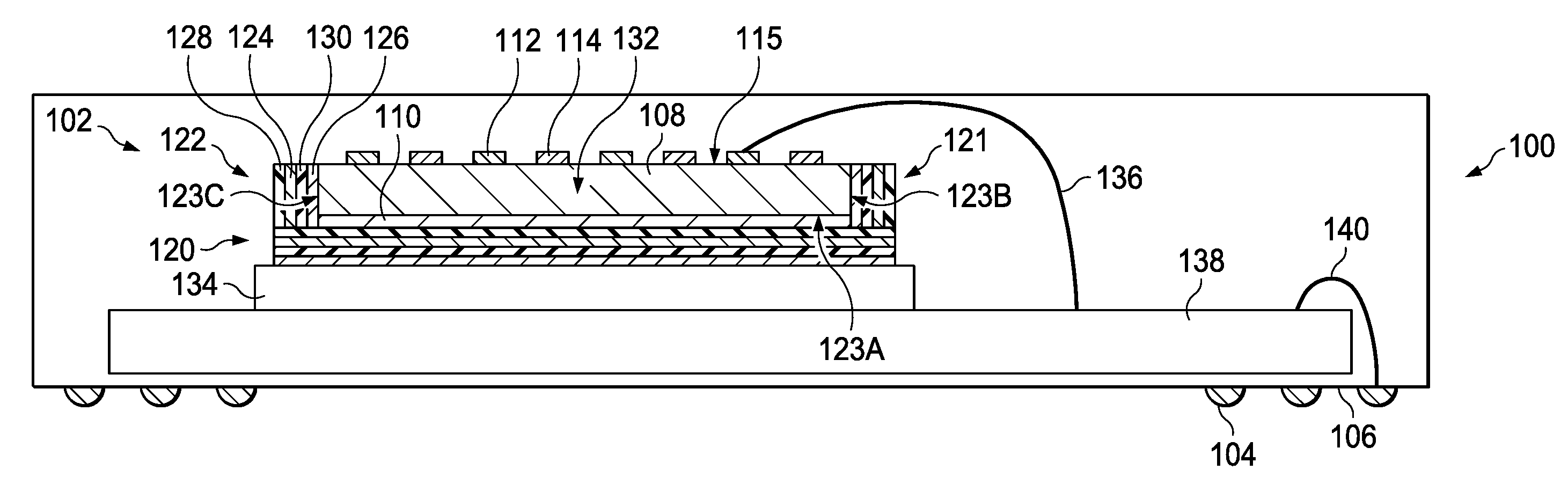
[0004] FIG. 1 is a side cross-section view of an example integrated circuit (IC) package including an example unreleased PAW resonator, constructed according to this disclosure.
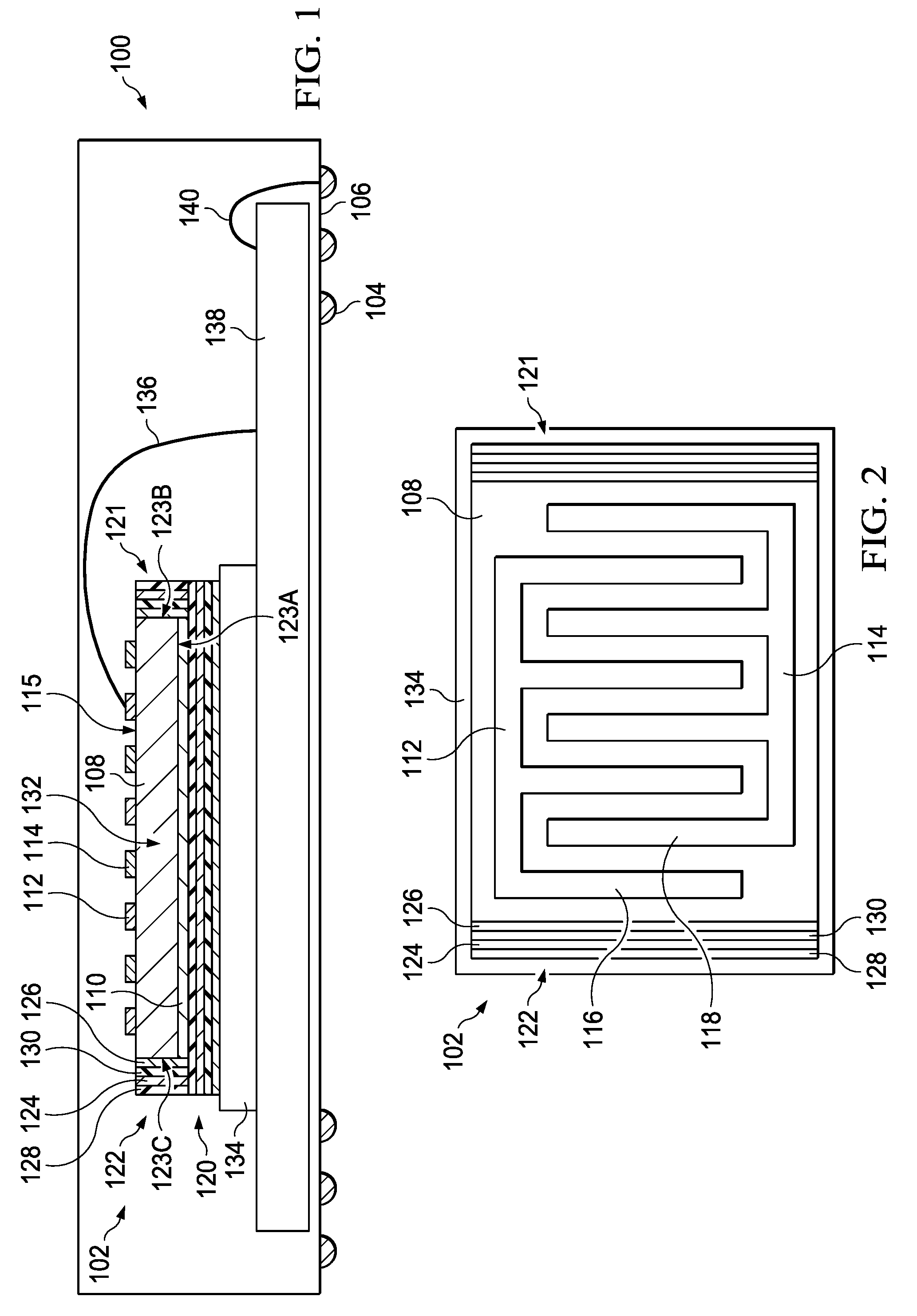
[0005] FIG. 2 is a top view of the example unreleased PAW resonator of FIG. 1.
[0006] The figures are not to scale. Instead, to clarify multiple layers and regions, the thickness of the layers may be enlarged in the drawings. Wherever possible, the same reference numbers will be used throughout the drawing(s) and accompanying written description to refer to the same or like parts. As used in this patent, stating that any part (e.g., a layer, film, area, or plate) is in any way positioned on (e.g., positioned on, located on, disposed on, or formed on, etc.) another part, indicates that the referenced part is either in contact with the other part, or that the referenced part is above the other part with one or more intermediate part(s) located therebetween. Stating that any part is in contact with another part means that there is no intermediate part between the two parts. Use of terms such as up, down, top, bottom, side, end, front, back, etc. herein are used with reference to a currently considered or illustrated orientation. If a different orientation is considered, such terms must be correspondingly modified. Connecting lines or connectors shown in the various figures presented are intended to represent example functional relationships and/or physical or logical couplings between the various elements.
DETAILED DESCRIPTION
[0007] The resonance frequency of bulk acoustic wave (BAW) resonators are determined, in part, by the thickness of their piezoelectric layer. In semiconductor implementations, piezoelectric layers are, by necessity, thin, which limits the range of frequencies implementable by BAW resonators. In contrast, the resonance frequencies of PAW resonators (a.k.a. contour mode resonators, or Lamb wave resonators) are determined, in part, by their lateral dimensions, for example, by the pitch of their interdigitated electrodes and the length and width of the piezoelectric layer. Accordingly, PAW resonators can implement a wider range of resonance frequencies than BAW resonators. However, known PAW resonators require the device to be released from (e.g., removed from, detached from, etc.) the substrate on which the PAW resonator is initially formed to confine acoustic energy in the PAW resonator, and then attached with tethers to other structures. Releasing a PAW resonator from a substrate can result in damage to the PAW resonator from mechanical stresses (e.g., vibration, shock, etc.). Moreover, released PAW resonator requires costly wafer-level packaging. The use of tethers may be unsuitable for high-power applications due to non-linear effects, and may cause high resistivity and heat dissipation issues.
[0008] Example unreleased PAW resonators that overcome at least these deficiencies of known PAW and BAW resonators are disclosed herein. The disclosed example unreleased PAW resonators include example acoustic reflectors (e.g., vertical and/or lateral) that confine acoustic energy in the unreleased PAW resonator, obviating the need to release the PAW resonator from the substrate on which it was formed. Thus, avoiding the disadvantages (e.g., mechanical stress, tethers, costly wafer-level packaging, limited heat dissipation, non-linearity, etc.) of known PAW resonators. In some disclosed examples, the unreleased PAW resonator is formed on a high-resistivity substrate that implements, among other things, a heat sink for the PAW resonator. In, for example, high power applications, the dissipation of heat improves the linearity of the PAW resonator.
[0009] In some examples, an unreleased PAW resonator, or variants thereof, means a PAW resonator that is intended to be, for all intents, formed (e.g., deposited, disposed, etc.) on a substrate to be permanently attached, coupled, connected, affixed, assembled or otherwise joined to the substrate in a way that is, by design, not intended for reversal. Even though an unreleased PAW resonator and substrate may be disassembled through, for example, sufficient knowledge, force, or tool does not negate the fact that they were intended, by design, to be fixedly assembled at manufacture of the unreleased PAW resonator. In stark contrast, released PAW resonators are, during manufacture, formed on a substrate, and then released (e.g., removed, detached, etc.) from the substrate.
[0010] Reference will now be made in detail to non-limiting examples of this disclosure, examples of which are illustrated in the accompanying drawings. The examples are described below by referring to the drawings.
[0011] FIG. 1 is a side cross-section view of an example IC package 100 having an example unreleased PAW resonator 102 disposed in the example IC package 100. FIG. 2 is a top view of the example PAW resonator 102 of FIG. 1. The example IC package 100 of FIG. 1 is a surface mount device with a plurality of contacts (an example of which is designated at reference numeral 104) on a bottom side 106. However, the example IC package 100 may be of any type, and may have any form, material(s), shape, dimension(s), number of contacts, shape of contacts, etc. Moreover, the unreleased PAW resonator 102 and/or any other components may be packaged, mounted, etc. in the IC package 100 in any way. The example IC package 100 may be, for example, a semiconductor-based device. In some examples, the IC package 100 is a wafer-level package, or a die-level package.
[0012] The example unreleased PAW resonator 102 of FIGS. 1 and 2 includes a piezoelectric layer 108 formed (e.g., deposited, disposed, etc.) on an example grounded electrode 110. In the case of a semiconductor-based IC package, the example piezoelectric layer 108 may include a piezoelectric material compatible with a semiconductor (e.g., complementary metal-oxide-semiconductor (CMOS)) manufacturing process, such as aluminum nitride (AlN), zinc oxide (ZnO), etc.
[0013] To excite acoustic waves in the unreleased PAW resonator 102, the example unreleased PAW resonator 102 of FIGS. 1 and 2 includes a first electrode 112 and a second electrode 114 on a top surface 115 of the piezoelectric layer 108. As shown in FIG. 2, the first electrode 112 includes a plurality of example fingers, one of which is designated at reference numeral 116, and the second electrode 114 includes a plurality of example fingers, one of which is designated at reference numeral 118. In the example of FIG. 2, the fingers 116 are interlaced with the fingers 118. Other electrodes having other configurations may be used. In the case of a semiconductor-based IC package, the example electrodes 110, 112 and 114 are formed of a conductive material compatible with a semiconductor manufacturing process.
[0014] To increase retention of acoustic energy in the unreleased PAW resonator 102, the example unreleased PAW resonator 102 includes an example horizontal (in the illustrated orientation of FIG. 1) acoustic reflector 120, and example vertical (in the illustrated orientation of FIG. 1) acoustic reflectors 121 and 122. Acoustic reflectors 120-122 are also known as dielectric mirrors, Bragg mirrors, etc. The example acoustic reflector 120 of FIG. 1 reduces acoustic energy leakage vertically through a bottom surface 123A of the piezoelectric layer 108. The example acoustic reflector 121 of FIGS. 1 and 2 reduces acoustic energy leakage laterally through the right end or edge 123B of the piezoelectric layer 108. The example acoustic reflector 122 of FIGS. 1 and 2 reduces acoustic energy leakage laterally through the left end or edge 123C of the piezoelectric layer 108.
[0015] Any known or future Bragg mirror, dielectric mirror, acoustic reflector, etc. may be used to implement the acoustic reflectors 120-122. The example acoustic reflectors 120-122 of FIGS. 1 and 2 include alternating layers of materials with different refractive indices. In some examples, the acoustic reflectors 120-122 include alternating flat conductive members (e.g., layers, sheets, plates, etc. of metal), two of which are designated at reference numerals 124 and 126, and flat dielectric members (e.g., layers, sheets, plates, etc. of a dielectric material), two of which are designated at reference numerals 128 and 130. The thickness(es) of and distances between the conductive members 124 and 126 are selected, based on an intended resonance frequency of the unreleased PAW resonator 102, to cause constructive interference at that frequency, resulting in the acoustic reflectors 120-122 reducing spurious modes, and confining (e.g., reflecting, directing, containing, etc.) at least some main mode of acoustic energy at that frequency in a resonant cavity portion 132 of the unreleased PAW resonator 102. In some examples, confining main mode acoustic energy refers to confining a portion of the main mode of acoustic energy. Thus, retention of acoustic energy at the intended resonance frequency in the unreleased PAW resonator 102 is increased, and the quality factor (Q) of the unreleased PAW resonator 102 is increased, and, in turn, the performance of a system including the example unreleased PAW resonator 102 and/or the example IC package 100. In some examples, the conductive members 124 and 126 include tungsten (W), titanium tungsten (TiW), or copper (Cu), and the dielectric members 128 and 130 includes silicon dioxide (SiO2), or a carbon doped oxide dielectric such as SiCOH, or aluminum nitride (AlN). In some examples, one or more of the acoustic reflectors 120-122 are implemented using a two-dimensional (2D) or a three-dimensional phononic crystal.
[0016] As shown in FIG. 1, the example acoustic reflector 120 is formed on example substrate 134 (e.g., a carrier wafer, etc.), forming the PAW resonator 102 as an unreleased PAW resonator 102. As shown in FIGS. 1 and 2, the acoustic reflectors 121 and 122 are disposed on the substrate 134 adjacent respective right and left (e.g., lateral) edges of the piezoelectric layer 108. Thus, the acoustic reflector 120 confines acoustic energy in the up-down direction, and the acoustic reflectors 121 and 122 confine acoustic energy in the lateral (e.g., right-left) directions. In some examples, the acoustic reflectors 121 and 122 can be omitted and use the air cavity as the lateral reflector. This configuration is also an unreleased PAW resonator since the resonator 102 is still attached on the vertical acoustic reflector 120 and the substrate 134. In some examples, the substrate 134 is formed of a high resistivity material, and the substrate 134 implements a heat sink for the unreleased PAW resonator 102, thus, improving the linearity of the unreleased PAW resonator 102 in, for example, high power applications.
[0017] The example electrodes 112 and 114 of FIGS. 1 and 2 may be electrically coupled with other components in the IC package 100 and/or external components. For example, the electrode 112 and/or the electrode 114 may be electrically coupled (shown conceptually by an example bone wire 136) to an IC 138 (e.g., a digital logic circuit, an analog circuit, a processor core, a digital signal processor (DSP) core, etc.) implemented in the IC package 100. In some examples, the IC 138 controls and/or uses a clock signal generated using the unreleased PAW resonator 102 to perform one or more functions (e.g., down conversion, up conversion, modulation, de-modulation, etc.). In some examples, the unreleased PAW resonator 102 is coupled with other acoustic resonators of different sizes to form a filtering function. The IC 138 and/or one of the electrodes 112 and 114 may be electrically coupled to the external contact 104, as shown in FIG. 1 with a bond wire 140. In some examples, the IC 138 is an IC die, and the unreleased PAW resonator 102 is a microelectromechanical system (MEMS) die.
[0018] The example acoustic reflectors 120-122 of FIGS. 1 and 2 may be formed using any number and/or type(s) of steps, processes, methods, etc. In some examples, the acoustic reflectors 120-122 are formed using conformal deposition to form alternating layers of metal and dielectric materials. In some examples, the acoustic reflectors 121 and 122 are formed by encompassing the piezoelectric layer 108 in a dielectric material, forming vertical trenches in the dielectric material to receive conductive material, filling the trenches with the conductive material, and then using chemical and mechanical polishing to remove excess conductive and dielectric materials.
[0019] While an example manner of implementing the IC package 100 including an unreleased PAW resonator 102, in accordance with this disclosure, is illustrated in FIGS. 1 and 2, one or more of the parts illustrated in FIGS. 1 and 2 may be combined, divided, re-arranged, omitted, eliminated and/or implemented in any other way. Further, an IC package including an unreleased PAW resonator having a convex surface in accordance with this disclosure may include one or more parts in addition to, and/or instead of, those illustrated in FIGS. 1 and 2, and/or may include more than one of any or all the illustrated parts. For example, acoustic reflectors may be included.
[0020] "Including" and "comprising" (and all forms and tenses thereof) are used herein to be open ended terms. Thus, whenever a claim lists anything following any form of "include" or "comprise" (e.g., comprises, includes, comprising, including, etc.), it is to be understood that additional elements, terms, etc. may be present without falling outside the scope of the corresponding claim. As used herein, when the phrase "at least" is used as the transition term in a preamble of a claim, it is open-ended in the same manner as the term "comprising" and "including" are open ended. Conjunctions such as "and," "or," and "and/or" are inclusive unless the context clearly dictates otherwise. For example, "A and/or B" includes A alone, B alone, and A with B. In this specification and the appended claims, the singular forms "a," "an" and "the" do not exclude the plural reference unless the context clearly dictates otherwise.
[0021] Any references, including publications, patent applications, and patents, cited herein are hereby incorporated by reference to the same extent as if each reference were individually and specifically indicated to be incorporated by reference and were set forth in its entirety herein.
[0022] Although certain example methods, apparatus and articles of manufacture have been disclosed herein, the scope of coverage of this patent is not limited thereto. On the contrary, this patent covers all methods, apparatus and articles of manufacture fairly falling within the scope of the claims of this patent.
* * * * *
D00000
D00001
XML
uspto.report is an independent third-party trademark research tool that is not affiliated, endorsed, or sponsored by the United States Patent and Trademark Office (USPTO) or any other governmental organization. The information provided by uspto.report is based on publicly available data at the time of writing and is intended for informational purposes only.
While we strive to provide accurate and up-to-date information, we do not guarantee the accuracy, completeness, reliability, or suitability of the information displayed on this site. The use of this site is at your own risk. Any reliance you place on such information is therefore strictly at your own risk.
All official trademark data, including owner information, should be verified by visiting the official USPTO website at www.uspto.gov. This site is not intended to replace professional legal advice and should not be used as a substitute for consulting with a legal professional who is knowledgeable about trademark law.