Ceramic Antenna Molds
HOSSEINI; Alister
U.S. patent application number 16/038106 was filed with the patent office on 2019-02-14 for ceramic antenna molds. The applicant listed for this patent is Energous Corporation. Invention is credited to Alister HOSSEINI.
| Application Number | 20190052115 16/038106 |
| Document ID | / |
| Family ID | 59088494 |
| Filed Date | 2019-02-14 |


| United States Patent Application | 20190052115 |
| Kind Code | A1 |
| HOSSEINI; Alister | February 14, 2019 |
CERAMIC ANTENNA MOLDS
Abstract
An example antenna may include: (i) an electromagnetic band gap (EBG) ground plane, and (ii) a dipole antenna, coupled with a via that extends to the EBG ground plane, configured to transmit a wireless power signal having a wavelength to a wireless power receiver, the dipole antenna being positioned approximately one-quarter of the wavelength above the EBG ground plane. Furthermore, the via is configured to conduct the wireless power signal, and the wireless power receiver is configured to convert the wireless power signal into usable power.
| Inventors: | HOSSEINI; Alister; (Phoenix, AZ) | ||||||||||
| Applicant: |
|
||||||||||
|---|---|---|---|---|---|---|---|---|---|---|---|
| Family ID: | 59088494 | ||||||||||
| Appl. No.: | 16/038106 | ||||||||||
| Filed: | July 17, 2018 |
Related U.S. Patent Documents
| Application Number | Filing Date | Patent Number | ||
|---|---|---|---|---|
| 15059354 | Mar 3, 2016 | 10027159 | ||
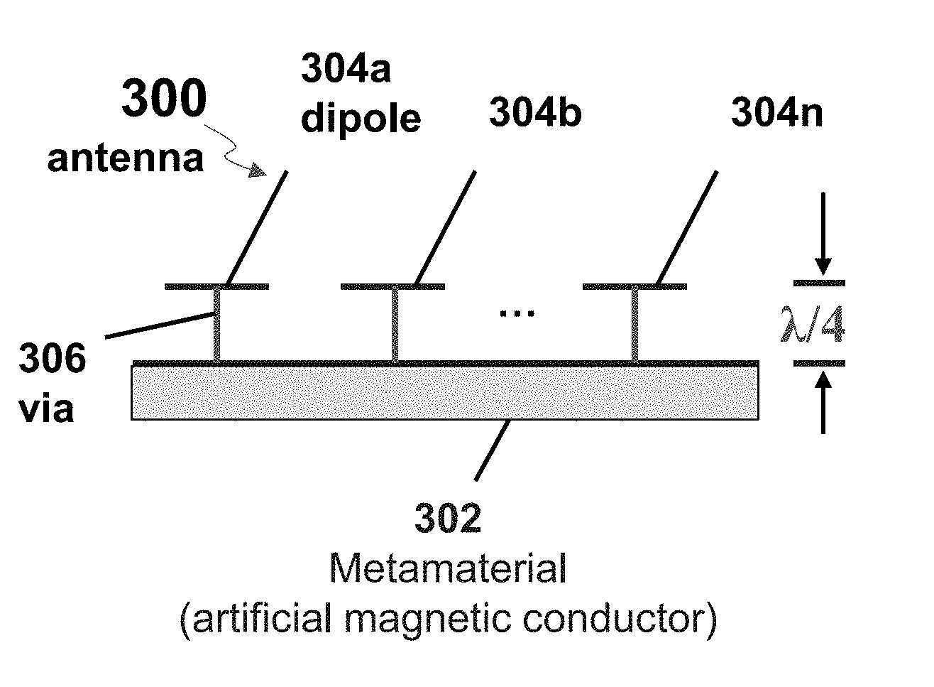
| 16038106 | ||||
| 62387207 | Dec 24, 2015 | |||
| Current U.S. Class: | 1/1 |
| Current CPC Class: | H02J 7/025 20130101; H02J 7/0042 20130101; H02J 50/23 20160201 |
| International Class: | H02J 7/02 20060101 H02J007/02; H02J 7/00 20060101 H02J007/00; H02J 50/23 20060101 H02J050/23 |
Claims
1. (canceled)
2. An antenna comprising: an electromagnetic band gap (EBG) ground plane; and a dipole antenna, coupled with a via that extends to the EBG ground plane, configured to transmit a wireless power signal having a wavelength to a wireless power receiver, the dipole antenna being positioned approximately one-quarter of the wavelength above the EBG ground plane, wherein: the via is configured to conduct the wireless power signal, and the wireless power receiver is configured to convert the wireless power signal into usable power.
3. The antenna of claim 2, further comprising a plurality of unit cells, periodically spaced apart from each other, formed over the EBG ground plane, wherein the dipole antenna is part of one of the plurality of unit cells.
4. The antenna of claim 2, wherein the dipole antenna is a dipole-slot antenna.
5. The antenna of claim 2, wherein the dipole antenna is a dual-polarized dipole antenna.
6. The antenna of claim 2, wherein the dipole antenna is configured to transmit the wireless power signal with a frequency in a range between 900 MHz to 100 GHz.
7. The antenna of claim 2, wherein the dipole antenna is embedded within a ceramic.
8. The antenna of claim 2, wherein the ceramic is composed of a silica.
9. The antenna of claim 3, further comprising a plurality of dipole antennas, each coupled with a respective via that extends to the EBG ground plane, configured to transmit wireless power signals each having a wavelength to the wireless power receiver, each of the plurality of dipole antennas being positioned approximately one-quarter of the wavelength above the EBG ground plane.
10. The antenna of claim 9, wherein the EBG ground plane comprises a metamaterial configured to reduce cross-coupling between adjacent dipole antennas of the plurality of dipole antennas respectively included in the plurality of unit cells.
11. The antenna of claim 10, further comprising: a plurality of metallic walls configured to separate the plurality of unit cells, wherein: each metallic wall is disposed between adjacent unit cells of the plurality of unit cells, and each metallic wall is configured to operate as a waveguide to reduce cross-coupling between adjacent dipole antennas of the plurality of dipole antennas.
12. A method of manufacturing an antenna, comprising: forming an electromagnetic band gap (EBG) ground plane; forming a via that extends from the EBG ground plane; and forming a dipole antenna that is: (i) coupled to the via and (ii) positioned approximately one-quarter of the wavelength above the EBG ground plane, the dipole antenna being configured to transmit a wireless power signal having a wavelength to a wireless power receiver, wherein: the via is configured to conduct the wireless power signal, and the wireless power receiver is configured to convert the wireless power signal into usable power.
13. The method of claim 12, further comprising forming a plurality of unit cells, periodically spaced from each other, formed over the EBG ground plane, wherein the dipole antenna is part of one of the plurality of unit cells.
14. The method of claim 12, wherein the dipole antenna is a dipole-slot antenna.
15. The method of claim 12, wherein the dipole antenna is a dual-polarized dipole antenna.
16. The method of claim 12, wherein the dipole antenna is configured to transmit the wireless power signal with a frequency in a range between 900 MHz to 100 GHz.
17. The method of claim 12, wherein the dipole antenna is embedded within a ceramic.
18. The method of claim 13, further comprising: forming a plurality of vias; and forming a plurality of dipole antennas, each of which is (i) coupled to one of the plurality of vias and (ii) positioned approximately one-quarter of the wavelength above the EBG ground plane, the plurality of dipole antennas being configured to transmit a plurality of wireless power signals each having a wavelength to the wireless power receiver.
19. The method of claim 18, wherein the EBG ground plane comprises a metamaterial configured to reduce cross-coupling between adjacent dipole antennas of the plurality of dipole antennas respectively included in the plurality of unit cells.
20. The method of claim 19, further comprising: forming a plurality of metallic walls configured to separate the plurality of unit cells, wherein: each metallic wall is disposed between adjacent unit cells of the plurality of unit cells, and each metallic wall is configured to operate as a waveguide to reduce cross-coupling between adjacent dipole antennas of the plurality of dipole antennas.
21. A method of manufacturing an antenna, comprising: forming a dipole antenna configured to transmit a wireless power signal having a wavelength to a wireless power receiver, coupling the dipole antenna to a via extending from an electromagnetic band gap (EBG) ground plane, the dipole antenna being positioned approximately one-quarter of the wavelength above the EBG ground plane, wherein: the via is configured to conduct the wireless power signal, and the wireless power receiver is configured to convert the wireless power signal into usable power.
Description
CROSS-REFERENCE TO RELATED APPLICATIONS
[0001] This application is a continuation of U.S. patent application Ser. No. 15/059,354, filed on Mar. 3, 2016, entitled "Antenna For Transmitting Wireless Power Signals," which claims the benefit of U.S. Provisional Patent Application Ser. No. 62/387,207, entitled "Ceramic Antenna Molds," filed Dec. 24, 2015, each of which is herein fully incorporated by reference in its respective entirety.
TECHNICAL FIELD
[0002] The subject matter disclosed herein generally relates to wireless charging systems, and in particular, to transmitter antennas that transmitter wireless power signals used to power electronic devices.
BACKGROUND
[0003] Wireless charging of batteries of electronic devices has historically been performed by using inductive coupling. A charging base station receiver of an electronic device may have one or more coils in which a current may be applied to produce a magnetic field such that when another coil is placed in close proximity, a transformer effect is created and power is transferred between the coils. However, such inductive coupling has a limited short range, such as a few inches or less. Examples of such wireless charging include electronic toothbrushes that are placed on a charging stand and inductive pads inclusive of one or more coils to enable electronic devices with coil(s) to be placed on the pads to be charged.
[0004] While inductive charging is helpful to eliminate users having to plug power cords into electronic devices for charging, the limited range at which electronic devices have to be positioned from charging stations is a significant shortcoming of the inductive charging technology. For example, if a user of a mobile device, such as a mobile telephone, is in a conference room without a charging pad or sufficient number of charging pads, then the user is unable to charge his or her phone without a traditional power cord.
[0005] Remote wireless charging has recently been developed. Remote wireless charging operates by generating a wireless signal carrying sufficient power that can be directed to charge a battery of an electronic device or to operate the wireless device. Such technology, however, has been limited due to technology advancements being a challenge, as transmitters, receivers, antennas, communications protocols, and intelligence of transmitters have all had to be developed (i) so that sufficient wireless power is able to be wirelessly directed to charge electronic devices and (ii) so that the remote wireless charging is effective and safe for people.
[0006] Electronic devices are becoming smaller and as such, receivers and antennas for receiving wireless power to charge the electronic devices are also to become smaller. Such receivers and antennas are to be able to receive multi-polarized wireless power signals in order to be more efficient in receiving and charging wireless power signals. One problem that exists with smaller antennas is that their efficiency can become lower especially as an array of closely spaced antennas are used in receiving RF signals.
SUMMARY
[0007] To provide for a receiver antenna that is small and efficient, an antenna configured with a plurality of unit cells with a metamaterial ground plane may be utilized. The metamaterial ground plane may include a magnetic conductor, such as a perfect magnetic conductor (PMC) or artificial magnetic conductor (AMC), as understood in the art. Such metamaterials may include FR4.
[0008] One embodiment of an embodiment of an antenna may include an electromagnetic band gap (EBG) ground plane, and a plurality of unit cells that are periodically spaced and inclusive of respective dipole antennas, and positioned over the EBG ground plane.
[0009] One embodiment of a method of manufacturing an antenna may include forming an electromagnetic band gap (EBG) ground plane, and forming a plurality of unit cells that are periodically spaced and inclusive of respective dipole antennas, and positioned over the EBG ground plane.
[0010] Additional features and advantages of an embodiment will be set forth in the description which follows, and in part will be apparent from the description. The objectives and other advantages of the invention will be realized and attained by the structure particularly pointed out in the exemplary embodiments in the written description and claims hereof as well as the appended drawings.
[0011] It is to be understood that both the foregoing general description and the following detailed description are exemplary and explanatory and are intended to provide further explanation of the invention as claimed.
BRIEF DESCRIPTION OF THE DRAWINGS
[0012] The accompanying drawings constitute a part of this specification and illustrate an embodiment of the invention and together with the specification, explain the invention.
[0013] FIG. 1 is an illustration of an illustrative wireless power environment in which transmitters may be configured to identify locations of are one or more receivers inclusive of dipole antennas that utilize metamaterials, and to communicate wireless power signals to those receiver(s) to form energy pocket(s) thereat, according to an exemplary embodiment.
[0014] FIG. 2 is an illustration of an antenna inclusive of a plurality of unit cells on which dipole antennas are utilized, according to an exemplary embodiment.
[0015] FIG. 3 is an illustration of an antenna inclusive of a plurality of unit cells on which dipole antennas are utilized, according to an exemplary embodiment.
[0016] FIG. 4 is an illustration of an antenna inclusive of a plurality of Yagi dipole antennas embedded within a ceramic are disposed, according to an exemplary embodiment.
[0017] FIG. 5 is an illustration of an illustrative antenna inclusive of a plurality of slot dipole antennas, according to an exemplary embodiment.
[0018] FIG. 6 is a flow diagram of an illustrative process for manufacturing an antenna, according to an exemplary embodiment.
DETAILED DESCRIPTION
[0019] The present disclosure is herein described in detail with reference to embodiments illustrated in the drawings, which form a part here. Other embodiments may be used and/or other changes may be made without departing from the spirit or scope of the present disclosure. The illustrative embodiments described in the detailed description are not meant to be limiting of the subject matter presented here. Alterations and further modifications of the inventive features illustrated herein, and additional applications of the principles of the inventions as illustrated herein, which would occur to one skilled in the relevant art and having possession of this disclosure, are to be considered within the scope of the invention.
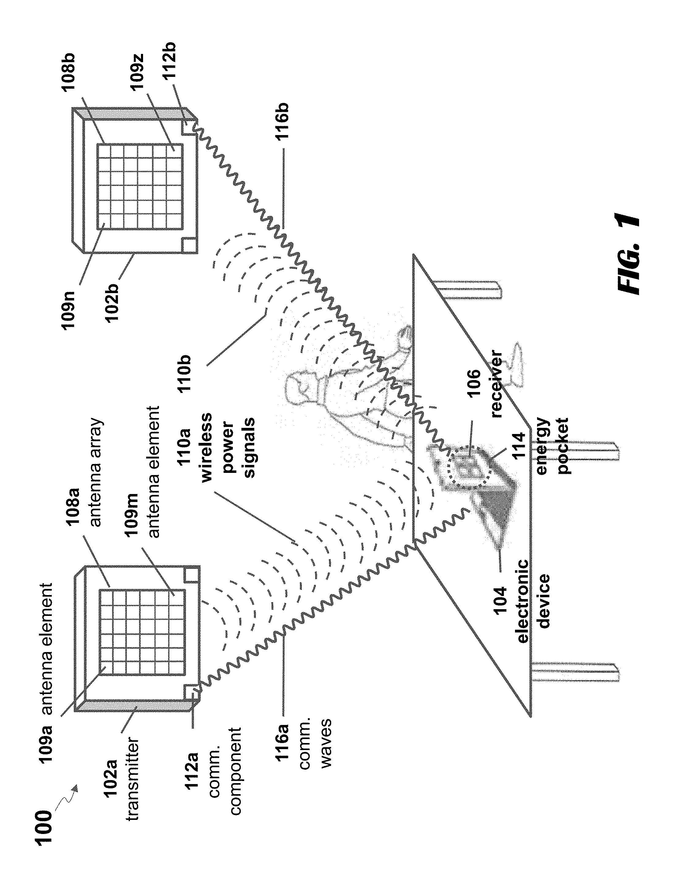
[0020] Referring to FIG. 1, an illustration of an illustrative wireless power environment 100 in which transmitters 102a, 102b (collectively 102) are configured to identify a location of an electronic device 104 with a receiver 106 (or multiple receivers) inclusive of one or more receiver antennas (e.g., cross-polarized dipole antenna), and transmit wireless power signals or waves to the receiver 106 to cause RF signal anti-nodes to form at the receiver 106 is shown. Although the wireless power environment is shown with multiple transmitters 102, it should be understood that a single transmitter may be utilized. The transmitters 102 each include antenna arrays 108a, 108b (collectively 108) inclusive of respective antenna elements 109a-109m, 109n-109z (collectively 109), and used to transmit wireless power signals 110a, 110b (collectively 110). In one embodiment, the antenna arrays 108a, 108b have the same number of antenna elements. Alternatively, the antenna arrays 108a, 108b have a different number of antenna elements. Still yet, the antenna arrays 108a, 108b may have the same or different layouts or configurations of antenna elements. The antenna arrays 108a, 108b may have regularly spaced antenna elements or multiple sets of antenna elements with different spacings that are used for different types of transmissions.
[0021] Because the transmitters 102 may be positioned in households and commercial settings, such as conference rooms, the transmitters 102 are to be sized in a manner that results in a small footprint and/or profile. Although the size of the footprint (e.g., width of overall antenna arrays) in some cases has to have a certain length for creating small energy pockets at various distances, the profiles (e.g., length of the antenna elements 109 along the z-axis, which defines the distance that the transmitters 102 extend from a wall) can be reduced to be more commercially viable for adoption by consumers and businesses.
[0022] The transmitters 102 may also include communication components 112a, 112b (collectively 112) that communicate with the electronic device 104. In one embodiment, the receiver 106 may be configured with a transmitter or other circuitry that enables communication with the communication components 112, thereby enabling the transmitters 102 to focus the wireless power signals 110 at the receiver 106 to form an energy pocket 114. The energy pocket 114 may be a localized region at which waves from the wireless power signals 110 form an anti-node (i.e., alignment and therefore constructive addition of peaks of wireless power waves) that produces a combination of peak signals from each of the wireless power signals 110, as understood in the art.
[0023] Because the antenna arrays 108 may have orientations that cause the wireless power signals 110 to be transmitted at different polarizations depending on an orientation of the electronic device with respect to the respective antenna arrays 108, the receiver 106 may include a dual-polarized dipole antenna, for example, so that orientation of the receiver 106 with respect to the antenna arrays 108 has minimal impact in the amount of power that is received from the wireless power signals 110.
[0024] With regard to FIG. 2, an illustration of an antenna 200 inclusive of a plurality of unit cells 204a-204n (collectively 204) on which dipole antennas are utilized is shown. The antenna may include a metamaterial for a ground plane 202. For example, the ground plane may be an EBG ground plane. The EBG ground plane may be formed of FR4 material. As understood, the EBG ground plane limits the amount of the backscatter radiation, and may be used to mimic a perfect magnetic conductor (PMC) over a finite frequency range. The unit cells may each include an antenna element, such as a dipole. The dipole may be a dual dipole and may be disposed in a periodic manner. In one embodiment, the dipole may be positioned one-quarter wavelength above the EBG ground plane. If the antenna is configured as a receiver antenna, the antenna may be low-profile due to the properties of the EBG ground plane. The antenna configuration may utilize the same or similar configuration principles as provided in co-pending U.S. patent application Ser. No. 14/925,374, entitled "Antenna for Wireless Charging Systems," which is hereby incorporated by reference in its entirety. If the antenna is configured to transmit RF signals, the antenna element may be a 31) antenna element embedded within a substrate, such as a ceramic. The ceramic may be composed of silica. Whether configured as a receiver or transmitter antenna, the use of the metamaterial for the ground plane 202 enables a reduction in size and improvement in performance of the antenna 200.
[0025] With regard to FIG. 3, an illustration of an antenna 300 inclusive of a plurality of unit cells on which dipole antennas are utilized is shown. The antenna 300 is shown to include a an EBG ground plane 302 composed of a metamaterial. The EBG ground plane may be an artificial magnetic conductor (AMC). Multiple dipole antennas 304 may be positioned above the ground plane 302 at one-quarter wavelength. Spacing of the multiple dipole antennas 30 may be closely separated and be periodic. As shown, a via 306 may extend below the dipole antennas and be connected to the EBG ground plane. As understood in the art, the use of a conventional ground plane and closely spaced antenna causes cross-coupling of signals between antennas, and, hence, a drop of power by several decibels (e.g., 3 dBs), which causes a drop in transmit power by 50%. The use of metamaterials, however, causes lower cross-coupling between adjacent antennas, such that overall power of the antenna 300 may be increased by 50% or more as compared to conventional antennas. In being unit cells, metallic walls (not shown) or other structure that define and separate the unit cells may be utilized. The metallic walls may operate as waveguide walls, thereby further reducing cross-coupling between antennas 304.
[0026] With regard to FIG. 4, an illustration of an antenna 400 configured to operate as a transmitter antenna may be inclusive of a plurality of 3D antennas 402 embedded within a ceramic 404 is shown. The 3D antennas 402 shown are Yagi dipole antennas. The ceramic may be used to reduce the size of the 3D antennas 402. The 3D antennas 402 may be printed or otherwise disposed on a printed circuit board (PCB). Alternatively, the 3D antennas 402 may be a wire configured as a dipole disposed within a ceramic or otherwise supported. In one embodiment, the antennas may be helical antennas embedded within a ceramic or any other antenna type embedded within a ceramic, as described in co-pending U.S. patent application Ser. No. 14/882,185, entitled "3D Ceramic Mold Antenna," may be utilized and is hereby incorporated by reference in its entirety. In another embodiment, a flat, cross-polarized antenna, as described in co-pending U.S. patent application Ser. No. 14/882,146, entitled "Cross-Polarized Dipole Antenna," may be utilized and is hereby incorporated by reference in its entirety. As a result of the ceramic in which resonator members are embedded, cross-coupling that would otherwise result due to the high reflection properties of the EBG ground plane 406 are substantially reduced, thereby providing for higher directivity and gain of the overall antenna. The 3D antennas 402 may be disposed on an EBG ground plane 406, as previously described.
[0027] In an embodiment, the wireless RF signal is over 1 GHz. However, the antenna can be configured to operate at frequencies in a range from 900 MHz to 100 GHz. More specifically, the center frequency may be about 1 GHz, 5.8 GHz, 24 GHz, 60 GHz, and 72 GHz with bandwidths suitable for operation (e.g., 200 MHz-5 GHz bandwidths), and the dimensions of the antenna may be configured to accommodate the frequencies of operation.
[0028] With regard to FIG. 5, an illustration of an illustrative antenna 500 inclusive of a plurality of slot dipole antennas is shown. The antenna 500 includes a metamaterial ground plane 502, where the metamaterial is an EBG ground plane. The metamaterial ground plane 502 may have a substrate beneath the metamaterial layer. Multiple, periodically spaced slot dipoles 504 may be positioned above the metamaterial ground plane 502. The positioning may be one-quarter wavelength of the RF signal above the metamaterial ground plane 502. Within the slot dipoles 504 may be elements 506 that define the slot dipoles 504. As shown, the slot dipoles 504 may be circular, and the elements 506 are circular. Alternative shapes, such as oval, may be used to define a slot dipole. A via (not shown) that extends from elements 506 and/or outside the elements within each of the unit cells may be connected to the metamaterial ground plane 502. Again, the configuration of the slot antenna with the EBG ground plane may use the same or similar principles and configurations as those described in co-pending U.S. patent application Ser. No. 14/925,469, entitled, "Antenna for Wireless Charging Systems."
[0029] With regard to FIG. 6, a flow diagram of an illustrative process 600 for manufacturing an antenna as described herein is shown. The process 600 starts at step 602 at which an electromagnetic band gap (EBG) ground plane may be formed. The EBG may be formed of a variety of EBG materials, such as FR4 material. The EBG materials may be artificial magnetic conductor. At step 604, multiple unit cells that are periodically spaced and inclusive of respective dipole antennas, and positioned over the EBG ground plane may be formed. The unit cells may be cells that are defined by a structure, such as metallic walls, that define and separate unit cells that are adjacent to one another. Each of the unit cells may have an antenna, such as a dipole or dual dipole antenna, that is used to receive RF signals. A via extending from the antenna, such as a dual dipole, may connect to the EBG ground plane. The RF signals may be over 1 GHz, and be wireless power signals that may be used to charge a battery or otherwise power an electronic device. The dipole may be disposed one-quarter wavelength above the EBG ground plane. If the antenna is a transmit antenna, a 3D antenna embedded within a substrate, such as a ceramic, may be disposed over the EBG ground plane.
[0030] The foregoing method descriptions and the process flow diagrams are provided merely as illustrative examples and are not intended to require or imply that the steps of the various embodiments must be performed in the order presented. The steps in the foregoing embodiments may be performed in any order. Words such as "then," "next," etc. are not intended to limit the order of the steps; these words are simply used to guide the reader through the description of the methods. Although process flow diagrams may describe the operations as a sequential process, many of the operations can be performed in parallel or concurrently. In addition, the order of the operations may be re-arranged. A process may correspond to a method, a function, a procedure, a subroutine, a subprogram, etc. When a process corresponds to a function, its termination may correspond to a return of the function to the calling function or the main function.
[0031] The preceding description of the disclosed embodiments is provided to enable any person skilled in the art to make or use the present invention. Various modifications to these embodiments will be readily apparent to those skilled in the art, and the generic principles defined herein may be applied to other embodiments without departing from the spirit or scope of the invention. Thus, the present invention is not intended to be limited to the embodiments shown herein but is to be accorded the widest scope consistent with the following claims and the principles and novel features disclosed herein.
* * * * *
D00000
D00001
D00002
D00003
D00004
XML
uspto.report is an independent third-party trademark research tool that is not affiliated, endorsed, or sponsored by the United States Patent and Trademark Office (USPTO) or any other governmental organization. The information provided by uspto.report is based on publicly available data at the time of writing and is intended for informational purposes only.
While we strive to provide accurate and up-to-date information, we do not guarantee the accuracy, completeness, reliability, or suitability of the information displayed on this site. The use of this site is at your own risk. Any reliance you place on such information is therefore strictly at your own risk.
All official trademark data, including owner information, should be verified by visiting the official USPTO website at www.uspto.gov. This site is not intended to replace professional legal advice and should not be used as a substitute for consulting with a legal professional who is knowledgeable about trademark law.