Chip Package Structure, Terminal Device, and Method
Zhou; Yibao ; et al.
U.S. patent application number 16/079459 was filed with the patent office on 2019-02-14 for chip package structure, terminal device, and method. The applicant listed for this patent is Guangdong Oppo Mobile Telecommunications Corp. Ltd.. Invention is credited to Wenzhen Zhang, Yibao Zhou.
| Application Number | 20190051574 16/079459 |
| Document ID | / |
| Family ID | 56396038 |
| Filed Date | 2019-02-14 |

| United States Patent Application | 20190051574 |
| Kind Code | A1 |
| Zhou; Yibao ; et al. | February 14, 2019 |
Chip Package Structure, Terminal Device, and Method
Abstract
A chip package apparatus includes a substrate, a chip on the substrate, and a filling layer on the substrate and surrounding a portion of the chip. The filling layer is made of epoxy molding compound (EMC) and the EMC is white. An electronic device with the chip package apparatus and a method for manufacturing the chip apparatus structure are provided.
| Inventors: | Zhou; Yibao; (Dongguan, Guangdong, CN) ; Zhang; Wenzhen; (Dongguan, Guangdong, CN) | ||||||||||
| Applicant: |
|
||||||||||
|---|---|---|---|---|---|---|---|---|---|---|---|
| Family ID: | 56396038 | ||||||||||
| Appl. No.: | 16/079459 | ||||||||||
| Filed: | April 6, 2017 | ||||||||||
| PCT Filed: | April 6, 2017 | ||||||||||
| PCT NO: | PCT/CN2017/079593 | ||||||||||
| 371 Date: | August 23, 2018 |
| Current U.S. Class: | 1/1 |
| Current CPC Class: | G06K 9/00053 20130101; H01L 23/562 20130101; H01L 2224/12105 20130101; H01L 2224/73265 20130101; H01L 2224/45144 20130101; H01L 23/488 20130101; H01L 2224/48091 20130101; H01L 2224/1601 20130101; H01L 24/16 20130101; H01L 24/32 20130101; H01L 23/3185 20130101; H01L 27/14678 20130101; H01L 2224/13101 20130101; H01L 2224/18 20130101; H01L 2224/32225 20130101; H01L 2224/16225 20130101; G06K 9/00006 20130101; H01L 23/29 20130101; H01L 2924/186 20130101; H01L 23/3121 20130101; H01L 2224/48225 20130101; H01L 24/48 20130101; H01L 24/45 20130101; H01L 24/13 20130101; H01L 24/96 20130101; H01L 21/56 20130101; H01L 2224/45144 20130101; H01L 2924/00014 20130101; H01L 2224/13101 20130101; H01L 2924/014 20130101; H01L 2924/00014 20130101; H01L 2224/48091 20130101; H01L 2924/00014 20130101 |
| International Class: | H01L 23/31 20060101 H01L023/31; H01L 23/00 20060101 H01L023/00; H01L 21/56 20060101 H01L021/56; G06K 9/00 20060101 G06K009/00 |
Foreign Application Data
| Date | Code | Application Number |
|---|---|---|
| Apr 8, 2016 | CN | 201610219333.2 |
Claims
1. A chip package apparatus, comprising: a substrate; a chip on the substrate; and a filling layer on the substrate and surrounding a portion of the chip, and the filling layer being made of epoxy molding compound and the epoxy molding compound being white.
2. The chip package apparatus of claim 1, wherein the chip is coupled with the substrate through solder balls, and the solder balls are disposed on the substrate in array.
3. The chip package apparatus of claim 1, wherein the chip is coupled with the substrate through conductive wires.
4. The chip package apparatus of claim 3, wherein the chip and the substrate are adhesively coupled through transparent optical adhesive.
5. The chip package apparatus of claim 2, wherein each solder ball has a diameter ranging from 0.22 mm to 0.3 mm or a distance between neighbor solder balls ranges from 0.46 mm to 0.55 mm.
6. The chip package apparatus of claim 1, wherein the chip package apparatus further comprises a reinforcement member disposed on the substrate to avoid the warpage of the substrate.
7. The chip package apparatus of claim 6, wherein the thermal conductivity of the reinforcement member is greater than that of the substrate.
8. The chip package apparatus of claim 6, wherein the substrate and the reinforcement member are adhesively coupled through transparent optical adhesive.
9. An electronic device, comprising: a white panel glass; and a chip package apparatus attached to the white panel glass, the chip package apparatus comprising: a substrate; a chip on the substrate; and a filling layer on the substrate and surrounding a portion of the chip, and the filling layer being made of epoxy molding compound and the epoxy molding compound being white.
10. The electronic device of claim 9, wherein the chip is coupled with the substrate through solder balls, and the solder balls are disposed on the substrate in array.
11. The electronic device of claim 9, wherein the chip is coupled with the substrate through conductive wires.
12. The electronic device of claim 11, wherein the chip and the substrate are adhesively coupled through transparent optical adhesive.
13. The electronic device of claim 10, wherein each solder ball has a diameter ranging from 0.22 mm to 0.3 mm or a distance between neighbor solder balls ranges from 0.46 mm to 0.55 mm.
14. The electronic device of claim 9, wherein the chip package apparatus further comprises a reinforcement member disposed on the substrate to avoid the warpage of the substrate.
15. The electronic device of claim 14, wherein the thermal conductivity of the reinforcement member is greater than that of the substrate.
16. The electronic device of claim 14, wherein the reinforcement member and the substrate are adhesively coupled through transparent optical adhesive.
17. The chip package apparatus of claim 2, wherein each solder ball has a diameter ranging from 0.22 mm to 0.3 mm and a distance between neighbor solder balls ranges from 0.46 mm to 0.55 mm.
18. A method for manufacturing a chip package electronic device, comprising: providing a substrate; disposing a chip on the substrate; and disposing a filling layer surrounding a portion of the chip on the substrate, the filling layer being made of epoxy molding compound, and the epoxy molding compound being white.
19. The method of claim 18, wherein solder balls are formed between the chip and the substrate, and each solder ball has a diameter ranging from 0.22 mm to 0.3 mm or a distance between neighbor solder balls ranges from 0.46 mm to 0.55 mm.
20. The method of claim 18, wherein the chip package apparatus further comprises a reinforcement member disposed on the substrate to avoid the warpage of the substrate, and the thermal conductivity of the reinforcement member is greater than that of the substrate.
Description
CROSS-REFERENCE TO RELATED APPLICATION(S)
[0001] This application claims priority to Chinese Patent Application No. 201610219333.2, filed on Apr. 8, 2016, the content of which is herein incorporated by reference in its entirety.
TECHNICAL FIELD
[0002] The present disclosure relates to the technology field of chip package, and more particularly, to a chip package apparatus, an electronic device with the chip package apparatus, and a method for manufacturing the chip package apparatus.
BACKGROUND
[0003] Electronic devices have entered the era of surface mount technology (SMT). With the development of miniaturization of electronic devices, the outlines of the SMT components have gradually miniaturized.
[0004] With the progress of science and technology, fingerprint recognition has become the standard of smart phones, tablet computers, and other terminal devices. At present, fingerprint unit chips (also known as fingerprint module chips) have a variety of shapes, such as round, square, rectangle and so on. In practical applications, packaging a fingerprint unit chip or other chips needs to consider various factors, such as performance, cost, appearance, and so on. It can be seen that how to provide a chip package apparatus with quick response has become an urgent problem to be solved.
SUMMARY
[0005] The technical problem to be solved in the embodiments of the present disclosure is to provide a chip package apparatus with quick response, an electronic device with the chip package apparatus, and a method for manufacturing the chip package apparatus.
[0006] In a first aspect, an embodiment of the present disclosure provides a chip package apparatus. The chip package apparatus includes a substrate, a chip on the substrate, and a filling layer on the substrate and surrounding a portion of the chip. The filling layer is made of an epoxy molding compound and the epoxy molding compound is white.
[0007] In a second aspect, an embodiment of the present disclosure provides an electronic device. The electronic device includes a white panel glass, and a chip package apparatus attached to the white panel glass. The chip package apparatus includes a substrate, a chip, and a filling layer. The chip is on the substrate. The filling layer is on the substrate and surrounds a portion of the chip. The filling layer is made of an epoxy molding compound and the epoxy molding compound is white.
[0008] In a third aspect, an embodiment of the present disclosure provides a method for manufacturing a chip package apparatus. The method includes providing a substrate, disposing a chip on the substrate, and disposing a filling layer surrounding a portion of the chip on the substrate. The material of the filling layer is epoxy molding compound and the epoxy molding compound is white.
BRIEF DESCRIPTION OF THE DRAWINGS
[0009] To better illustrate the technical solutions of embodiments of the present disclosure or of the prior art, the following descriptions will briefly illustrate the accompanying drawings described in the embodiments or in the prior art. Obviously, the following described accompanying drawings are merely some embodiments of the present disclosure. Those skilled in the art can obtain other accompanying drawings according to the described accompanying drawings without creative efforts.
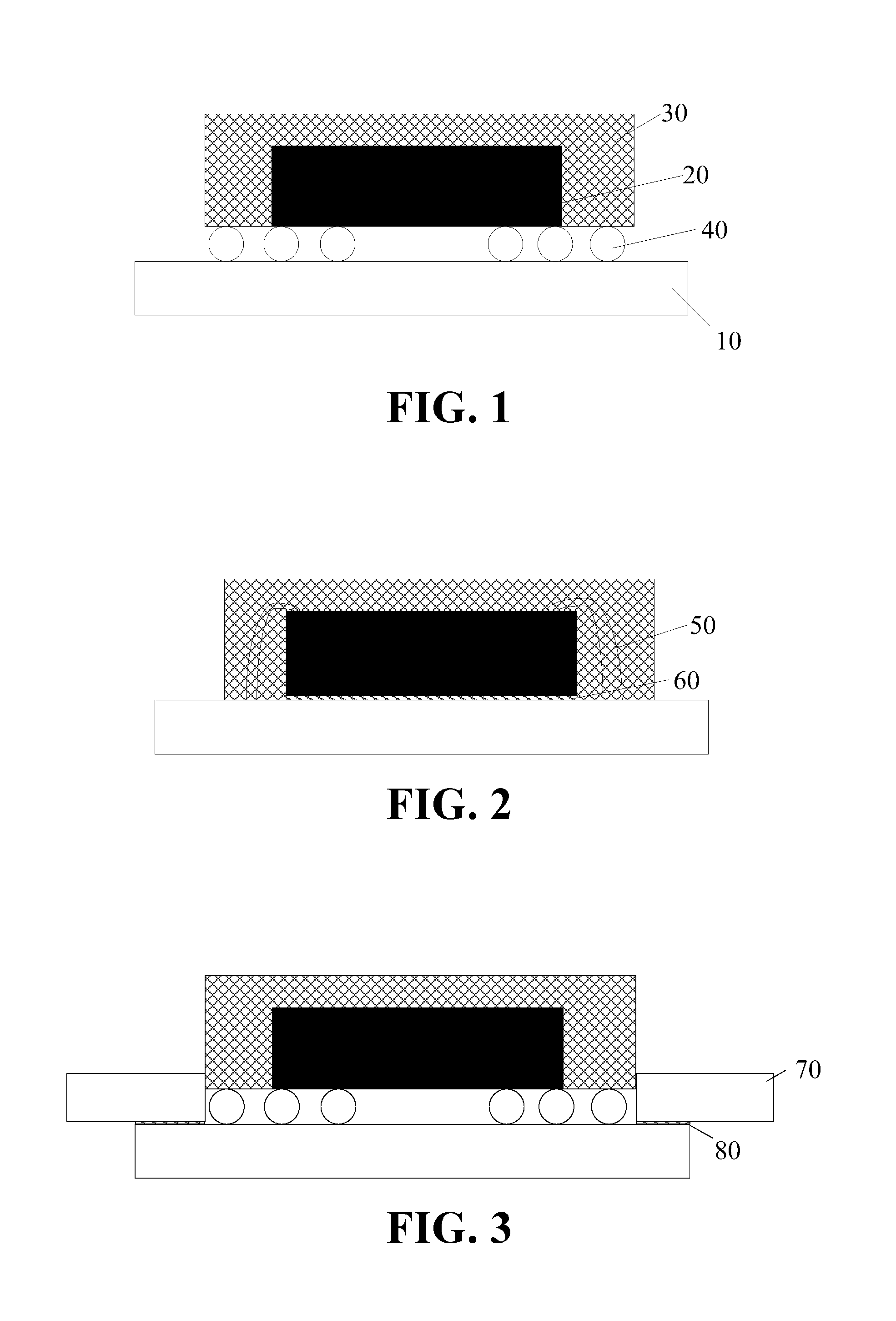
[0010] FIG. 1 is a schematic cross-sectional view of a chip package apparatus according to a first embodiment of the present disclosure.
[0011] FIG. 2 is a schematic cross-sectional view of a chip package apparatus according to a second embodiment of the present disclosure.
[0012] FIG. 3 is a schematic cross-sectional view of a chip package apparatus according to a third embodiment of the present disclosure.
[0013] FIG. 4 is a schematic view of an electronic device with a chip package apparatus according to an embodiment of the present disclosure.
[0014] FIG. 5 is a flow chart of a method for manufacturing a chip package apparatus according to an embodiment of the present disclosure.
DETAILED DESCRIPTION
[0015] In order to enable those skilled in the art to better understand the solutions of the present disclosure, the technical solutions of embodiments of the present disclosure will be described clearly and completely in combination with the accompanying drawings of the embodiments of the present disclosure. Obviously, the described embodiments are merely a part of embodiments of the present disclosure, but not all of the embodiments. All other embodiments obtained by those skilled in the art without creative efforts based on the embodiments of the present disclosure shall fall within the protection scope of the present disclosure.
[0016] Unless defined otherwise, technical or scientific terms used herein should be interpreted as a generic meaning understood by those skilled in the art. Terms "first", "second", "third", "fourth" and so on used in the present disclosure are used to distinguish different objects, rather than describe any specific sequence, quantity, or importance. Similarly, terms such as "a", "an" or "the" do not denote a limitation of quantity, but are used to indicate at least one. Similarly, the term "include" or "comprise" and the like means that the element or object that appears ahead of the word covers the element or object that appears after the word and its equivalent, and does not exclude other elements or objects. The term "couple" or the like is not limited to physical or mechanical connections, but may include electrical connections, whether direct or indirect. The terms "up", "down", "left", "right" and the like are only used to represent relative positional relationships. When the absolute position of the described object is changed, the relative positional relationship may also be changed accordingly.
[0017] For clarity, the thickness of layers or regions in the drawings is enlarged rather than according to the actual scale. When an element such as a layer, a film, a region, or a substrate and the like is referred to as being "on" another element, the element may be "directly" on another element or an intervening element may exist.
[0018] The "embodiment" mentioned herein means that particular features, structures, or characteristic described with reference to the embodiments may be included in at least one embodiment of the present disclosure. Phrases appearing at various positions of the specification neither always refer to the same embodiment, nor separate or alternative embodiments that are mutually exclusive with other embodiments. It is explicitly and implicitly understood by those skilled in the art that the embodiments described herein may be combined with other embodiments.
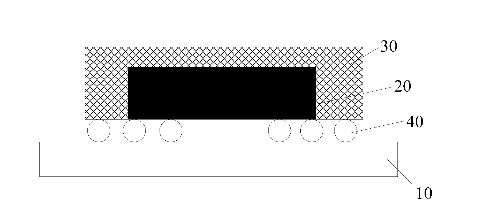
[0019] FIG. 1 is schematic cross-sectional views of a chip package apparatus according to a first embodiment of the present disclosure. The chip package apparatus includes a substrate 10, a chip 20, a filling layer 30. The chip 20 is disposed on the substrate 10. The filling layer 30 is disposed on the substrate 10 and surrounds a portion of the chip 20. The material of the filling layer 30 is epoxy molding compound (EMC) and the EMC is white. It can be seen that as the filling layer 30 is white, when the chip package apparatus is applied to an electronic device with a white panel glass, a surface cover of the chip (such as a fingerprint chip or other chips) need not be provided with an ink layer. This may omit a process and reduce the cost. In addition, as the thickness of the ink layer is reduced, a distance from the finger to the chip becomes shorter, and the entire response of capacitors and the strength of signals become stronger. The electronic device may obtain information with better quality. It is beneficial to enhance the response speed of the electronic device.
[0020] Therein, the substrate 10 may include a dielectric material, such as organic material. The organic material may be at least one of polypropylene (PP), epoxy resin, polyimide. The filling layer 30 may prevent the chip 20 from being damaged and/or being contaminated. The chip 20 is a fingerprint unit chip (also known as fingerprint module chip). Of course, the chip 20 may be other chips.
[0021] In at least one implementation, the chip package apparatus may further include another substrate. The substrate may be, such as but not limited to, a print circuit board. The substrate 10 and the chip 20 may be disposed on a top surface of another substrate. In one embodiment, a thickness of the substrate 10 may be less than that of another substrate.
[0022] In at least one implementation, the chip package apparatus may further include a conductive member. The conductive member is disposed between another substrate and the chip 20. Electrical signals may be transferred between another substrate and the chip 20 through the conductive member.
[0023] In at least one implementation, the chip 20 is coupled with the substrate 10 through solder balls 40. The solder balls 40 are disposed on the substrate 10 in an array (also known as arrayed solder balls).
[0024] In at least one implementation, each solder ball 40 has a diameter ranging from 0.22 mm to 0.3 mm.
[0025] In at least one implementation, the distance between neighbor solder balls 40 ranges from 0.46 mm to 0.55 mm.
[0026] Therein, the distance between neighbor solder balls 40 may be equal or not equal. For example, the distance between the outmost row of the arrayed solder balls and the secondary outmost row of the arrayed solder balls is less than that between other neighbor rows of the solder balls, and the distance between the outmost column of the arrayed solder balls and the secondary outmost column of the arrayed solder balls is less than that between other neighbor columns of the solder balls. For example, the distance between neighbor rows of the solder balls in array gradually increases along a direction towards or away from a center of the chip package apparatus, and the distance between neighbor columns of the solder balls in array gradually increases along the direction of the center towards or away from the chip package apparatus, and so on, which is not limited in the present disclosure.
[0027] FIG. 2 is a schematic cross-sectional view of a chip package apparatus according to a second embodiment of the present disclosure. The chip package apparatus of the second embodiment is similar to the chip package apparatus of the first embodiment except that the chip 20 is adhesively coupled with (also known as adhesively bonded to) the substrate 10 through transparent optical adhesive 60 and conductive wires 50. The conductive wires 50 may be selected from a group consisting of gold wires, silver wires, and copper wires.
[0028] Therein, in the structure of the chip 20 coupled with the substrate 10 through conductive wires 50, in order to enhance the reliability and the structural stability of the chip package apparatus, the substrate 10 and the chip 20 are adhesively coupled through the transparent optical adhesive 60. Of course, the optical adhesive 60 may be replaced by other glues with the functions of adhesive bonding, which is not limited in the present disclosure.
[0029] FIG. 3 is a schematic cross-sectional view of a chip package apparatus according to a third embodiment of the present disclosure. The chip package apparatus of the third embodiment is similar to the chip package apparatus of the first embodiment except that a reinforcement member 70 is adhesively coupled with the substrate 10 through transparent optical adhesive 80.
[0030] In at least one implementation, the thermal conductivity of reinforcement member 70 is greater than that of the substrate 10.
[0031] In at least one implementation, the reinforcement member 70 extends from an edge of the substrate 10.
[0032] Therein, based on the demand for lightness, thinness, and integration of electronic devices, the size of the chip package apparatus has been continuously reduced. The thickness of the substrate 10 is reduced accordingly. For example, the thickness of the substrate 10 may range from 100 .mu.m.about.200 .mu.m, or range from 20 .mu.m.about.80 .mu.m. As the thickness of the substrate 10 is reduced, the structural strength of the substrate 10 is accordingly decreased. The substrate 10 supporting the chip 20 may exist a problem of the warpage such that the step of disposing the substrate on other electronic components is difficult to be implemented. Therefore, the reliability and the structural stability of the chip package apparatus are insufficient. To enhance the reliability and the structural stability of the chip package apparatus, the reinforcement member 70 is disposed on the substrate 10 to avoid the warpage of the substrate 10. In addition, the thermal conductivity of the reinforcement member 70 is greater than that of the substrate 10. In this way, not only the reliability and the structural stability of the chip package apparatus are reinforced, but also the heat dissipation of the chip 20 during operation is improved. The reinforcement member 70 may include, but not limited to, stainless steel, copper, aluminum, gold, silver, alloys of different metal material, or combinations of the foregoing. In order to enhance the adhesively coupling between the reinforcement member 70 and the substrate 10, the reinforcement member 70 and the substrate 10 may be adhesively coupled through the transparent optical adhesive 80. Of course, the transparent optical adhesive 80 may be replaced by other glues, which is not limited in the present disclosure.
[0033] FIG. 4 is a schematic structural view of an electronic device according to an embodiment of the present disclosure. In FIG. 4, "A" denotes the chip package apparatus illustrated in FIGS. 1 to 3 and "B" denotes a white panel glass. The chip package apparatus may be attached to the white panel glass, for example, the chip package apparatus may be disposed below the white panel glass or in an opening of the white panel glass. In the embodiment, the chip package apparatus may be disposed in the opening of the white panel glass. The chip package apparatus includes a substrate 10, a chip 20, a filling layer 30. The chip 20 is disposed on the substrate 10. The filling layer 30 is disposed on the substrate 10 and surrounds a portion of the chip 20. The material of the filling layer 30 is epoxy molding compound (EMC) and the EMC is white.
[0034] Therein, "mobile terminal" or "terminal device" referred in the embodiments of the present disclosure is also referred to user equipment (UE), which is a kind of device providing voice and/or data communication to the user, such as handheld devices having wireless communication functions, in-vehicle devices, and so on. The common electronic device, such as, includes, mobile phones, tablet computers, notebook computers, palm computers, mobile internet devices (MIDs), wearable devices, such as smart watches, and smart wristbands.
[0035] In at least one implementation, the chip 20 is coupled with the substrate through solder balls 40. The solder balls 40 are disposed on the substrate 10 in the array.
[0036] In at least one implementation, each the solder ball 40 has a diameter ranging from 0.22 mm to 0.3 mm.
[0037] In at least one implementation, a distance between neighbor solder balls 40 ranges from 0.46 mm to 0.55 mm.
[0038] In at least one implementation, the chip 20 is coupled with the substrate 10 through conductive wires 50, such as gold wires, silver wires, copper wires, and so on.
[0039] In at least one implementation, the chip 20 and the substrate 10 are adhesively coupled through transparent optical adhesive 60.
[0040] In at least one implementation, the chip package apparatus further includes a reinforcement member 70 disposed on the substrate 10.
[0041] In at least one implementation, the thermal conductivity of reinforcement member 70 is greater than that of the substrate 10.
[0042] In at least one implementation, the substrate 10 and the reinforcement member 70 are adhesively coupled through transparent optical adhesive 80.
[0043] In at least one implementation, the reinforcement member 70 extends from an edge of the substrate 10.
[0044] It can be seen that in the embodiment, when the chip apparatus structure is applied to the electronic device with the white panel glass and the filling layer 30 is white, a surface cover of the chip (such as fingerprint chips or other chips) need not be provided with an ink layer. This may omit a process and reduce the cost. In addition, as the thickness of the ink layer is reduced, a distance from the finger to the chip becomes shorter, and the entire response of capacitors and the strength of signals become stronger. The electronic device may obtain information with better quality. It is beneficial to enhance the response speed of the electronic device.
[0045] FIG. 5 is a flow chart of a method for manufacturing a chip package apparatus according to an embodiment of the present disclosure. The method in the embodiment of the present disclosure may include the operations at blocks illustrated in FIG. 5.
[0046] At block 501, a substrate 10 is provided.
[0047] At block 502, a chip 20 is disposed on the substrate 10.
[0048] At block 503, a filling layer 30 is disposed on the substrate 10 and surrounds a portion of the chip 20. The filling layer 30 is made of epoxy molding compound (EMC) and the EMC is white.
[0049] In at least one implementation, solder balls 40 are disposed on the substrate 10 in the array to enable the chip 20 to be coupled with the substrate 10 through the solder balls 40.
[0050] In at least one implementation, conductive wires 50 are disposed between the substrate 10 and the chip 20 to enable the chip 20 to be coupled with the substrate 10 through the conductive wires 50. The conductive wires 50 may be selected from a group consisting of gold wires, silver wires, and copper wires.
[0051] In at least one implementation, in the structure of the chip 20 coupled with the substrate 10 through conductive wires 50, in order to enhance the reliability and the structural stability of the chip package apparatus, a transparent optical adhesive 60 is disposed between the substrate 10 and the chip 20 to adhesively couple the chip 20 and the substrate 10.
[0052] In at least one implementation, each solder ball 40 has a diameter ranging from 0.22 mm to 0.3 mm.
[0053] In at least one implementation, a distance between neighbor solder balls 40 ranges from 0.46 mm to 0.55 mm.
[0054] In at least one implementation, in order to enhance the reliability and the structural stability of the chip package apparatus, a reinforcement member 70 is disposed on the substrate 10 to avoid the warpage of the substrate 10.
[0055] In at least one implementation, in order to enhance heat dissipation of the chip 20 during operation, the thermal conductivity of reinforcement member 70 is set to be greater than that of the substrate 10.
[0056] In at least one implementation, in order to enhance the adhesive coupling between the substrate 10 and the reinforcement member 70, a transparent optical adhesive 80 is disposed between the substrate 10 and the reinforcement member 70 to adhesively couple the reinforcement member 70 and the substrate 10.
[0057] It can be seen that as the filling layer 30 is white, when the chip package apparatus is applied to a electronic device with a white panel glass, a surface cover of the chip (such as a fingerprint chip or other chips) need not to be provided with an ink layer. This may omit a process and reduce the cost. In addition, as the thickness of the ink layer is reduced, a distance from the finger to the chip becomes shorter, and the entire response of capacitors and the strength of signals become stronger. The electronic device may obtain information with better quality. It is beneficial to enhance the response speed of the electronic device.
[0058] The above embodiments are only used to illustrate the technical solution of the present disclosure rather than to limit the present disclosure. Referring to the foregoing embodiments, the present disclosure is described in detail, the skilled in art should understand that the technical solution recited in the foregoing embodiments may be modified or some technical features may be replaced equivalently, those modifications or replacements will not make the essence of the corresponding technical solutions deviate from the scope of the technical solutions of the embodiments of the present disclosure.
* * * * *
D00000
D00001
D00002
XML
uspto.report is an independent third-party trademark research tool that is not affiliated, endorsed, or sponsored by the United States Patent and Trademark Office (USPTO) or any other governmental organization. The information provided by uspto.report is based on publicly available data at the time of writing and is intended for informational purposes only.
While we strive to provide accurate and up-to-date information, we do not guarantee the accuracy, completeness, reliability, or suitability of the information displayed on this site. The use of this site is at your own risk. Any reliance you place on such information is therefore strictly at your own risk.
All official trademark data, including owner information, should be verified by visiting the official USPTO website at www.uspto.gov. This site is not intended to replace professional legal advice and should not be used as a substitute for consulting with a legal professional who is knowledgeable about trademark law.