Hand worn interface device
Hogbin; Matthew Richard William
U.S. patent application number 16/040536 was filed with the patent office on 2019-02-14 for hand worn interface device. This patent application is currently assigned to Matthew Richard William Hogbin. The applicant listed for this patent is Matthew Richard William Hogbin. Invention is credited to Matthew Richard William Hogbin.
| Application Number | 20190050052 16/040536 |
| Document ID | / |
| Family ID | 65015891 |
| Filed Date | 2019-02-14 |


| United States Patent Application | 20190050052 |
| Kind Code | A1 |
| Hogbin; Matthew Richard William | February 14, 2019 |
Hand worn interface device
Abstract
A wearable device comprises a flexible substrate carrying multiple conducting loops which are formed into a zig zag pattern so as to be able to accommodate a stretching of the substrate. The substrate is formed into a glove and the loops positioned such that they are aligned with the anatomical joints. As the anatomical joints move, the loops change shape and accordingly change their inductance--this is measured by the electronics in the glove and used to calculate the joint angles in a processor which transmits the angles to an external computer system. Some of the loops are attached to current drivers in the electronics module, and a magnet positioned close to the loop, providing means for a force to be generated between magnet and loop when the current driver passes current through the loop, thereby providing tactile feedback to the user.
| Inventors: | Hogbin; Matthew Richard William; (St Albans, GB) | ||||||||||
| Applicant: |
|
||||||||||
|---|---|---|---|---|---|---|---|---|---|---|---|
| Assignee: | Hogbin; Matthew Richard
William St Albans GB |
||||||||||
| Family ID: | 65015891 | ||||||||||
| Appl. No.: | 16/040536 | ||||||||||
| Filed: | July 19, 2018 |
Related U.S. Patent Documents
| Application Number | Filing Date | Patent Number | ||
|---|---|---|---|---|
| 62534413 | Jul 19, 2017 | |||
| 62535991 | Jul 24, 2017 | |||
| Current U.S. Class: | 1/1 |
| Current CPC Class: | G06F 3/014 20130101; G06F 3/0346 20130101; G01B 7/30 20130101; G01R 27/2611 20130101; G06F 3/016 20130101 |
| International Class: | G06F 3/01 20060101 G06F003/01; G06F 3/0346 20060101 G06F003/0346; G01R 27/26 20060101 G01R027/26 |
Claims
1} A wearable device providing means of body joint angle measurement comprising; a) A flexible, elastic substrate. b) Means for attaching said substrate to the body. c) Conductive loops mounted upon or within the substrate in positions aligned to body joints when the device is worn. d) Inductance measurement circuits attached to some or all of the conductive loops by means of conductive wires passing within or upon the garment. e) A processor attached to the inductance measuring circuits, providing means to collect the values together from each circuit and from the inductance values to calculate body joint angles.
2} The wearable device of claim 1 wherein said conductive loops are provided with zigzag edges so that they may expand as the corresponding body joint moves.
3} The wearable device of claim 1 wherein said conductive loops consist of multiple turns.
4} The wearable device of claim 1 wherein said conductive loops are positioned opposite the main direction of flexion of the corresponding body joint.
5} The wearable device of claim 2 wherein the device is attached to the users hand.
6} The wearable device of claim 5 wherein multiple hand joints are provided with one or more extensible conductive loops.
7} The wearable device of claim 6 wherein the metacarpal phalangeal joints of digits are provided with two extensible conductive loops placed opposite the primary direction of joint flexion and either side of
8} The wearable device of claim 1 wherein permanent magnets are placed in proximity to some of the conductive loops, and current driving circuitry attached to the loops, providing means to generate a current in the loops, so generating a force upon the magnet, thereby providing tactile feedback to the user.
9} The wearable device of claim 1 wherein said inductance measurement circuitry includes a capacitor, amplifier, feedback circuit and frequency counter connected to each said conductive loop, and an amplifier and feedback loop are connected to the combination of said conductive loop and said capacitor providing means for an oscillatory signal to be generated.
10} The wearable device of claim 5 wherein a structure is attached to the main garment passing partially or completely around the wrist, which comprises multiple optical or magnetic transmitters or receivers, able to interoperate with a tracking system providing means of locating the hand in three dimensional space.
11} The wearable device of claim 1 wherein said means for attaching said substrate to the body comprise tubular structures through which body parts can pass, which may include fasteners such that they can be
12} The wearable device of claim 1 wherein said flexible elastic substrate is a silicone or polyurethane elastomer, or is a woven elastic textile.
13} The wearable device of claim 1 wherein said processor is attached to a wireless transmitter providing means to relay the information from said processor back to a computer.
14. The wearable device of claim 9 wherein the ampifier, feedback circuit and frequency counter are realised within a Field Programmable Gate Array
Description
FIELD OF THE INVENTION
[0001] The present invention relates to computer human interface devices, and more specifically to interface devices can be worn on and which interface with parts of the human body such as the hand. Such devices are useful in interacting with computer programs, such as interacting three dimensional representations of objects or data, or in the context of virtual reality, and in capturing body motion for later replay.
BACKGROUND OF THE INVENTION
[0002] Some previous devices have used resistive flex sensors incorporating partially conductive elastomeric materials to measure the flexion of hand joints. These devices have the disadvantage that the value measured depends on the joint angle in a nonlinear way, and also upon previous joint angles, that is to say they display hysteresis. These devices have the further disadvantage that the value measured changes with temperature. These devices have the further disadvantage that they consist of several components--electrodes, active elastomeric medium, and a flexible substrate, as well as wires to carry signals to and from supporting circuitry, resulting in a relatively high overall cost.
[0003] Other previous devices have used optical fibres to measure the joint angles of the hand. These devices have the disadvantage that they require a light source, light transmission, and light detection, as well as analog amplification and analog to digital conversion circuitry, resulting in a high overall cost.
[0004] Other previous devices have used external optical means such as cameras to measure the joint angles of the hand, for instance devices available from Leap Motion. These devices have the disadvantage that they cannot always see every part of the hand, due to the blocking of one part of the hand by another in some poses and accordingly lose track of the position of the parts of the hand they cannot see. These devices also have the disadvantage that they cannot provide tactile feedback to the user as they are not in contact with the user's skin.
DRAWING DESCRIPTIONS
[0005] FIG. 1 shows the general layout of conductive loops within or upon a hand worn embodiment of the device and their placement with respect to the joints of the hand.
[0006] FIG. 2 shows a different view of the device, showing the placement of conductive loops around the joints of the thumb.
[0007] FIG. 3 shows a view from the palmar surface of the device.
[0008] FIG. 4 shows the conductive wires connecting the conductive loops with the electronics module.
[0009] FIG. 5 shows the conductive loops and connecting wires that are associated with a single digit, connected to the electronics module.
[0010] FIG. 6 shows a single conductive loop and it's associated connecting wires, connected to the electronics module.
[0011] FIG. 7 shows the electronic circuit associated with each conductive loop.
[0012] FIG. 8 shows one embodiment of the electronic circuit associated with each conductive loop.
[0013] FIG. 9 shows a structure mounted on the device and embedded with tracking transceivers.
DETAILED DESCRIPTION OF EMBODIMENTS
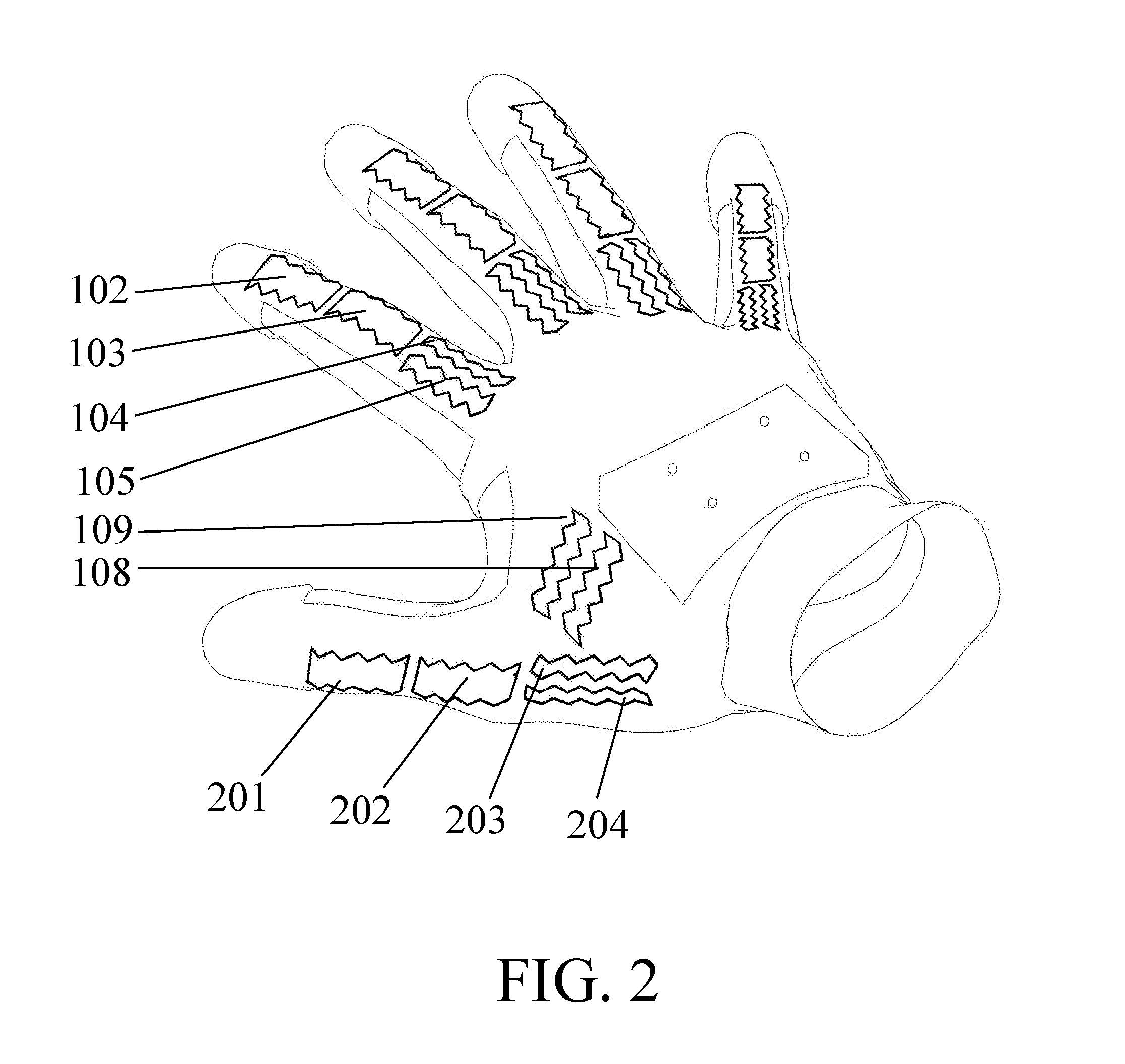
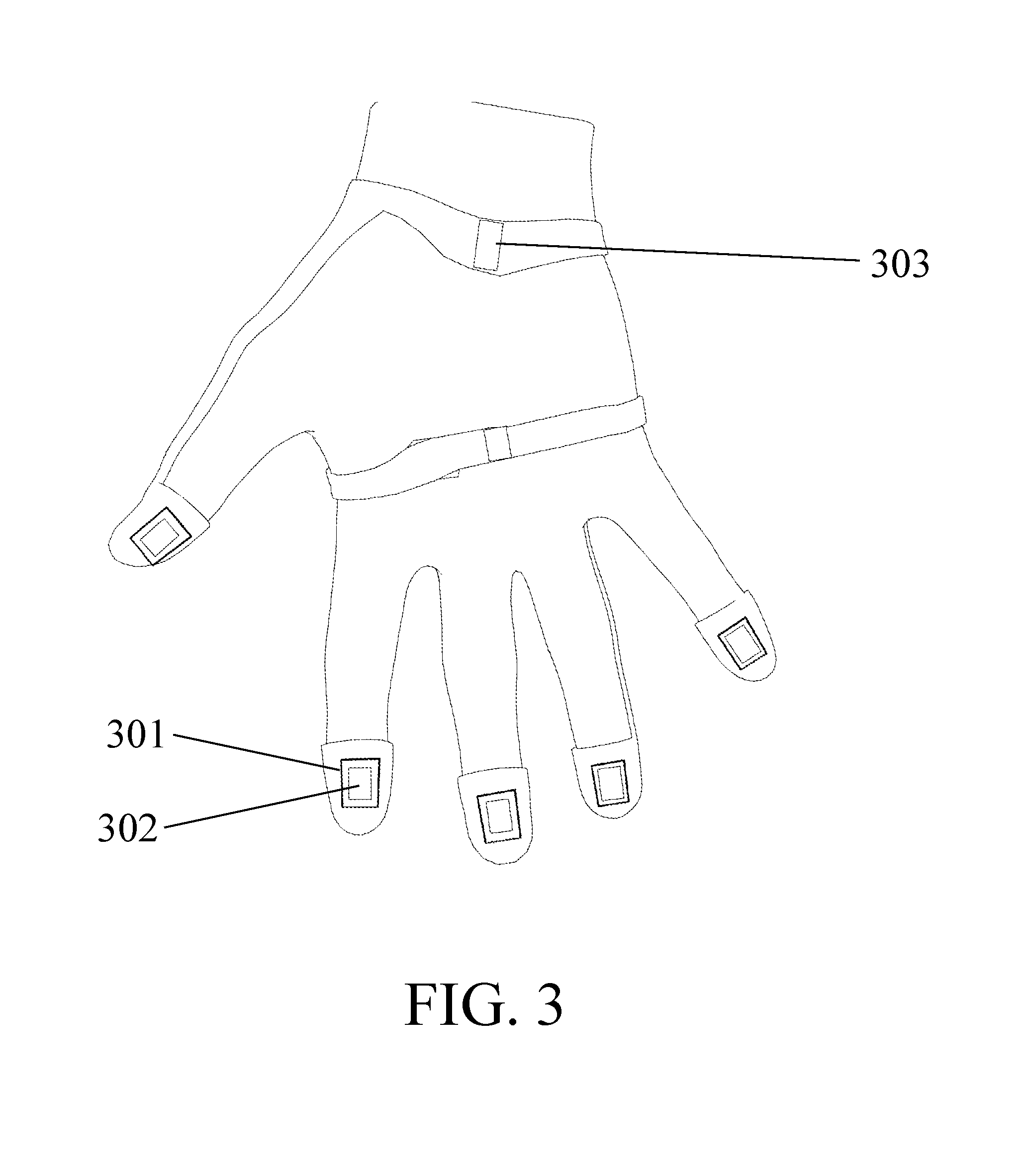
[0014] One embodiment of the device is shown in FIG. 1 (overview), FIG. 2 (thenar view), and FIG. 3 (palmar view). This embodiment of the device is worn on the hand but other embodiments may be worn on other parts of the body. A flexible, elastic substrate 101 is worn on the user's hand 110. Said substrate 102 may be made from an elastomer such as silicone or polyurethane, or a woven elastic textile such as Lycra.
[0015] Conductive loops 102, 103, 104, 105, 108 and 109 are mounted upon, woven into or embedded within said substrate 102. The basic structure for each finger, formed by the set up loops 102, 103, 104, 105, may be taken as being repeated for each digit as shown in the figure. In addition to the same four loops as the other digits, the thumb is also provided with two additional loops 108 and 109.
[0016] In some embodiments of the device the conductive loops 102, 103, 104, 105, 108 and 109 are made of metal wire such as copper which is of a thickness that they can bend repeatedly without breaking. In some embodiments the thickness of the copper wire is typically 0.1 mm.
[0017] An electronics module 106, houses inductance measurement electronics, a processor, a wireless transmitter and a battery and is mounted onto the substrate 102. Contacts (exemplified by 107) are provided as means to connect the device to an external power source in order to charge it's internal battery.
[0018] Conductive loop 102 is positioned on top of the distal interphalangeal joint of the digit, and the measurement of it's inductance is used to calculate the angle of this joint.
[0019] Conductive loop 103 is positioned on top of the proximal interphalangeal joint of the digit.
[0020] Conductive loops 104 and 105 are positioned on top of the metacarpal phalangeal joint.
[0021] Each conductive loop 102, 103, 104, 105, 108, 109 consists of zigzag edges such that it can accomodate a stretching of the substrate. When one of the finger joints flexes, the associated conductive loop is stretched and the inductance is increased. Conversely when a joint extends the inductance is decreased. The electronics module 106 uses this inductance change to calculate the joint flexion.
[0022] When a digit adducts or adbucts at the metacarpal phalangeal joint, loops 104 and 105 are stretched or compressed. The electronics module 106 uses the difference in the change in the change in inductance of loops 104 and 105 to calculate the degree of adduction or abduction of the digit.
[0023] In the same way, when the thumb carpal metacarpal joint flexes, loops 108 and 109 change inductance due to the twisting and bending motion imparted to the substrate between the thumb and the back of the hand. For this reason loops 108 and 109 are mounted close to the upper surface of the substrate, above the neutral axis of the material, to maximise this response.
[0024] The thumb is provided with conductive loops 201, 202, 203 and 204 which correspond to finger loops 102, 103, 104 and 105 respectively. In some embodiments loop 202 is replaced by a loop pair 203, 204 in order to measure adduction and abduction of the thumb metacarpal phalangeal joint. Loops 203 and 204 measure the thumb carpal metacarpal joint in the same way as described for the measurement of the finger metacarpal phalangeal joint using loops 104 and 105.
[0025] Magnets 302 are placed on the each of the fingertips close to conductive loops 301. The electronics module 106 includes current drivers attached to the coil. The electronics module 106 can receive a command from an external computer to drive a current in the coil 301, producing a force on the magnet 302 and creating a tactile feedback effect on the user's skin. In other embodiments the structure comprised of 301 and 302 can be replicated at other points of the skin surface in order to provide more detailed tactile feedback effects.
[0026] Fasteners 303 for attaching the wearable device may be provided to allow sections of the wearable device to be split apart and joined together, in order to make it easier to put on and take off.
[0027] FIG. 4 shows the zig-zag connecting wire pair 401 connecting the loop 102 with the electronics module 106. The zig zag connecting wire pair is so shaped to accomodate stretch in the same way as the conductive coils 102 themselves. Every conducting coil discussed has a similar conducting wire pair connecting it to the electronics module 106.
[0028] In other embodiments the coils 102, 103, 104, 105, 108 and 109 and connecting wires 401 may have alternate patterns such as wavy arcs in alternate directions, rounded zig zags, rectangular side to side patterns, or helical structures in order to allow them to acommodate stretching of the underlying and embedding substrate material.
[0029] FIG. 5 shows the detail of the layout of the coils for a single digit 102, 103, 104, 105 and 301 and their associated conducting wire pairs 501, 401, 504, 503 and 502 connecting each coil to the electronics module 106. This arrangement is repeated for each digit of the hand.
[0030] FIG. 6 shows a single coil in detail. Each coil discussed may consist of more than one turns of conductor. In one embodiment between three and five turns of inductor are used but other numbers of turns may be used without materially changing the invention. Each connecting wire pair 401 comprises a wire 601 and 602 such that the whole circuit runs in an unbroken circuit from the electronics module 106, down the wire 601, one or more times around the loop 102, and back down the wire 602 to the electronics module.
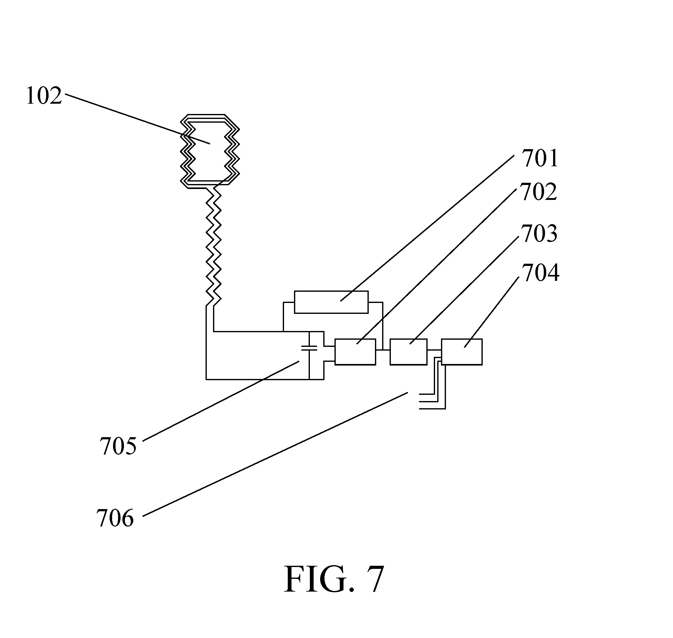
[0031] FIG. 7 shows the detail of a coil 102 connected to the electronics module 106, which is comprised of a capacitor 705, an amplifier 702, a feedback loop 701, a frequency counter 703, and a processor/wireless transmitter 704. The processor 704 has inputs 706 which are connected to the frequency counters associated with all the other coils in the system which require measurement. The basic arrangement comprising 705, 702, 702, and 703 is repeated for each coil; only the circuit for coil 102 is shown here for clarity.
[0032] In some embodiments, the amplifier 702, feedback loop 701, and frequency counter 703 are implemented inside a field programmable gate array such as a Lattice ICE40LP1K integrated circuit. In other embodiments the amplifier 702, feedback loop 701 and frequency counter 703 may be provided by an inductance to digital converter. In other embodiments the amplifier may be provided by one or more transistors or amplifier integrated circuits without materially changing the invention.
[0033] The processor 704, which may be realised as a Nordic NRF52832 as well as other possible equivalent parts, includes a wireless transmitter, using for example the Bluetooth wireless transmission standard, which relays the measured joint angles to an external computer. In some embodiments a proprietary protocol such as Nordic Enhanced Shockburst may be used as an alternative without materially changing the invention.
[0034] FIG. 8 shows an alternative embodiment of the electronics module 106 wherein a 4093 NAND Schmidt trigger is used to create the oscillator, and a capacitor 802 is placed differently to the capacitor 705 of FIG. 7.
[0035] FIG. 9 shows a tracking structure 901 mounted onto the electronics module 106 and electrically connected to the electronics module 106 via the electrical contacts 107. The tracking structure 901 passes partially or fully around the wrist and houses multiple tracking modules 902, for example implemented TS3633-CM1 provided by Triad Semiconductor. These receivers 902 provide the three dimensional position of the hand relative to an external frame of reference. In an alternative embodiment, the tracking modules 902 are realised as light emitting diodes and tracked by a camera external to the device, again for the purposes of 3 d tracking.
* * * * *
D00000
D00001
D00002
D00003
D00004
D00005
D00006
D00007
D00008
D00009
XML
uspto.report is an independent third-party trademark research tool that is not affiliated, endorsed, or sponsored by the United States Patent and Trademark Office (USPTO) or any other governmental organization. The information provided by uspto.report is based on publicly available data at the time of writing and is intended for informational purposes only.
While we strive to provide accurate and up-to-date information, we do not guarantee the accuracy, completeness, reliability, or suitability of the information displayed on this site. The use of this site is at your own risk. Any reliance you place on such information is therefore strictly at your own risk.
All official trademark data, including owner information, should be verified by visiting the official USPTO website at www.uspto.gov. This site is not intended to replace professional legal advice and should not be used as a substitute for consulting with a legal professional who is knowledgeable about trademark law.