Microstructure Separation Filters
Richardson; Brian Edward
U.S. patent application number 16/161678 was filed with the patent office on 2019-02-14 for microstructure separation filters. The applicant listed for this patent is Imagine TF, LLC. Invention is credited to Brian Edward Richardson.
| Application Number | 20190046897 16/161678 |
| Document ID | / |
| Family ID | 65274565 |
| Filed Date | 2019-02-14 |


View All Diagrams
| United States Patent Application | 20190046897 |
| Kind Code | A1 |
| Richardson; Brian Edward | February 14, 2019 |
Microstructure Separation Filters
Abstract
Microstructure separation filters are provided herein, as well as chromatography and other separation devices. An exemplary filter device includes a microstructure filter has a plurality of layers of alternating sacrificial and/or structural material which have been etched to create inlet channels and outlet channels. Adjacent ones of the inlet channels and the outlet channels are spaced apart from one another by cross channels that filter a fluid from the inlet channels to the outlet channels. The cross channels include filter features formed by etching away of a portion of the layers. The device also includes a housing configured to receive the microstructure filter.
| Inventors: | Richardson; Brian Edward; (Los Gatos, CA) | ||||||||||
| Applicant: |
|
||||||||||
|---|---|---|---|---|---|---|---|---|---|---|---|
| Family ID: | 65274565 | ||||||||||
| Appl. No.: | 16/161678 | ||||||||||
| Filed: | October 16, 2018 |
Related U.S. Patent Documents
| Application Number | Filing Date | Patent Number | ||
|---|---|---|---|---|
| 14846154 | Sep 4, 2015 | 10124275 | ||
| 16161678 | ||||
| 62179582 | May 11, 2015 | |||
| 62176125 | Feb 9, 2015 | |||
| 62123717 | Nov 25, 2014 | |||
| 62070778 | Sep 5, 2014 | |||
| Current U.S. Class: | 1/1 |
| Current CPC Class: | B01D 63/088 20130101; B01L 2300/0816 20130101; B01D 15/125 20130101; G01N 30/603 20130101; B01D 69/02 20130101; G01N 30/6069 20130101; B01L 2400/086 20130101; B01L 2300/0681 20130101; B01D 63/082 20130101; B01L 2300/0809 20130101; B01L 3/502753 20130101; B01D 67/0062 20130101; B01L 9/527 20130101; B01L 3/502707 20130101; B01L 2300/0803 20130101; B01D 15/22 20130101; B01D 2325/028 20130101; B01D 2325/08 20130101; G01N 30/6095 20130101 |
| International Class: | B01D 15/22 20060101 B01D015/22; B01D 67/00 20060101 B01D067/00; B01D 69/02 20060101 B01D069/02; B01L 3/00 20060101 B01L003/00; B01L 9/00 20060101 B01L009/00 |
Claims
1-20. (canceled)
21. A filter device, comprising: a microstructure filter comprising a plurality of layers of sacrificial material and an outer layer of structural material, the layers being etched to create inlet channels and outlet channels, wherein adjacent ones of the inlet channels and the outlet channels are spaced apart from one another by cross channels that filter a fluid flowing from the inlet channels to the outlet channels, the cross channels comprising filter features formed by etching away a portion of the sacrificial layers; wherein the plurality of layers of sacrificial material comprise: a base material; a first layer of sections of sacrificial material, the sections being spaced apart from one another equidistantly, the first layer being disposed on the base material; a second layer of sections of sacrificial material deposited on the first layer, the second layer comprising pairs of sections of sacrificial material offset from the sections of the first layer so as to cover spaces between the sections of the first layer; a third layer of sections of sacrificial material deposited on the second layer, the second layer comprising triplets of sections of sacrificial offset from the sections of the second layer; a fourth layer of sections of sacrificial material deposited on the third layer, wherein sections are contiguous and extend across half of the microstructure filter length; and the outer layer of structural material being disposed on the fourth layer of sections of sacrificial material; and a housing configured to receive the microstructure filter, the housing being configured to connect to a chromatograph device.
22. The filter device according to claim 21, wherein spaces are etched into the microstructure filter to create openings.
23. The filter device according to claim 21, wherein the cross channels comprise microstructure filter features formed by etching away a portion of the sacrificial layers, the microstructure filter features comprising nanostructures that increase a surface area of the filter features to attract particles present in the fluid as the fluid passes through the filter features from the inlet channels to the outlet channels.
24. The filter device according to claim 21, wherein the filter features comprise openings that are sized to capture a selected size of particles present in the fluid.
25. The filter device according to claim 21, wherein the microstructure filter comprises a plurality of spacer areas that provide structural support between adjacent ones of the plurality of layers of structural material, wherein the filter features are disposed between adjacent ones of the plurality of spacer areas.
26. The filter device according to claim 25, wherein adjacent ones of the plurality of spacer areas are offset from one another to stagger the filter features of adjacent layers of the plurality of layers.
27. The filter device according to claim 21, wherein the microstructure filter comprises an etched inlet section and an etched outlet section.
28. The filter device according to claim 21, wherein the housing is a tubular case that comprises an inner shell that receives the chromatograph device.
29. The filter device according to claim 21, wherein at least a portion of the filter features are provided with a nanoscale surface treatment to increase surface area of the filter features and thus an attractive force exerted by the filter features onto particles in the fluid.
30. The filter device according to claim 21, wherein the housing comprises a first connector that delivers fluid to the microstructure filter, wherein the first connector is configured to filter the fluid prior to entry into the microstructure filter.
31. The filter device according to claim 30, wherein the first connection is a frit comprising an outer peripheral sidewall that encircles a plurality of sections of passages.
32. The filter device according to claim 31, wherein the plurality of sections of passages are disposed in a ringed configuration and arranged such that passages of sections near a center of the frit have smaller diameter passages than passages of sections near the outer peripheral sidewall.
33. The filter device according to claim 31, wherein the plurality of sections of passages each comprise passages with unique spacing or diameters.
34. A filter device, comprising: a microstructure filter comprising cross channels that filter a fluid flowing from inlet channels to outlet channels, the cross channels comprising microstructure filter features formed by etching away a portion of the sacrificial layers; the microstructure filter features comprising nanostructures that increase a surface area of the filter features to attract particles present in the fluid as the fluid flows through the filter.
35. The filter device according to claim 34, wherein spaces are etched into the microstructure filter to create openings.
36. The filter device according to claim 34, wherein the microstructure filter comprises a plurality of spacer areas that provide structural support between adjacent ones of the plurality of layers of structural material, wherein the filter features are disposed between adjacent ones of the plurality of spacer areas.
37. The filter device according to claim 36, wherein adjacent ones of the plurality of spacer areas are offset from one another to stagger the filter features of adjacent layers of the plurality of layers.
38. The filter device according to claim 34, wherein the microstructure filter comprises an etched inlet section and an etched outlet section.
39. The filter device according to claim 34, wherein the housing is a tubular case that comprises an inner shell that receives the chromatograph device.
40. The filter device according to claim 34, wherein at least a portion of the filter features are provided with a nanoscale surface treatment to increase surface area of the filter features and thus an attractive force exerted by the filter features onto particles in the fluid.
Description
CROSS REFERENCE TO RELATED APPLICATIONS
[0001] This application claims the priority benefit of U.S. Provisional Application Ser. No. 62/070,778, filed Sep. 5, 2014; U.S. Provisional Application Ser. No. 62/123,717, filed Nov. 25, 2014; U.S. Provisional Application Ser. No. 62/176,125, filed on Feb. 9, 2015; and U.S. Provisional Application Ser. No. 62/179,582, filed May 11, 2015, all of which are hereby incorporated by reference herein in their entireties, including all references cited therein. This application is also related to U.S. patent application Ser. No. 14/701,528, filed on May 1, 2015, which is hereby incorporated by reference here in its entirety, including all references cited therein.
FIELD OF THE PRESENT TECHNOLOGY
[0002] The present technology relates generally to separation filters and chromatography, and more specifically, but not by limitation, to microstructure substrates that comprise micro-structured panels, complex flow orifices, and various types of filtering systems configured from these substrates, such as chromatography devices.
SUMMARY OF THE PRESENT TECHNOLOGY
[0003] According to some embodiments, the present technology may be directed to a chromatography or other type of separation device, comprising: (a) a microstructure filter comprising a plurality of layers of structural material which are spaced apart to create inlet channels and outlet channels, wherein adjacent ones of the inlet channels and the outlet channels are spaced apart from one another by cross channels that filter a fluid from the inlet channels to the outlet channels, the cross channels comprising filter features formed by removing a portion of the plurality of layers of the structural material; and (b) a housing configured to receive the microstructure filter, the housing being configured to connect to a device to test the fluid.
[0004] The present technology may be directed to a filter device, comprising: (a) a microstructure filter comprising a plurality of layers of sacrificial material and an outer layer of structural material, which have been etched to create inlet channels and outlet channels, wherein adjacent ones of the inlet channels and the outlet channels are spaced apart from one another by cross channels that filter a fluid from the inlet channels to the outlet channels, the cross channels comprising filter features formed by etching away of a portion of the sacrificial layers, wherein the plurality of layers of sacrificial material comprise: (i) a base material; (ii) a first layer of sections of sacrificial material are spaced apart from one another equidistantly, the first layer disposed on the base material; (iii) a second layer deposited on the first layer, the second layer comprising pairs of sections of sacrificial offset from the sections of the first layer so as to cover spaces between the sections of the first layer; (iv) a third layer deposited on the second layer, the second layer comprising triplets of sections of sacrificial offset from the sections of the second layer; (v) a fourth layer deposited on the third layer, wherein sections are contiguous and extend across half of the microstructure filter length; and (vi) the outer layer of structural material being disposed on the fourth layer; and (b) a housing configured to receive the microstructure filter, the housing being configured to connect to a chromatograph device to test the fluid.
[0005] According to still other embodiments, the present technology may be directed to a filter device, comprising: (a) a microstructure filter comprising cross channels that filter a fluid from inlet channels to outlet channels, the cross channels comprising microstructure filter features formed by etching away of a portion of the sacrificial layers, the microstructure filter features comprising nanostructures that increase a surface area of the filter features to attract particles present in the fluid as the fluid passes through the filter features from the inlet channels to the outlet channels; and (b) a housing configured to receive the microstructure filter, the housing being configured to connect to a chromatograph device to test the fluid.
BRIEF DESCRIPTION OF THE DRAWINGS
[0006] Certain embodiments of the present technology are illustrated by the accompanying figures. It will be understood that the figures are not necessarily to scale and that details not necessary for an understanding of the technology or that render other details difficult to perceive may be omitted. It will be understood that the technology is not necessarily limited to the particular embodiments illustrated herein.
[0007] FIG. 1 is an isometric view of the separation filter, constructed in accordance with the present technology.
[0008] FIG. 2 is an isometric view of the filter panel of FIG. 1.
[0009] FIG. 3 is a front view of the filter panel shown in FIG. 2.
[0010] FIG. 4 is a close-up front view of the microstructure area shown in FIG. 3.
[0011] FIG. 5 is an isometric view of the microstructure area shown in FIG. 4.
[0012] FIG. 6 is a close-up view similar to what is shown in FIG. 4 that includes fluid flow lines.
[0013] FIG. 7 is a close-up view similar to what is shown in FIG. 4 that shows an alternate embodiment.
[0014] FIG. 8 is a close-up view similar to what is shown in FIG. 4 that shows an alternate embodiment.
[0015] FIG. 9 is a close-up view similar to what is shown in FIG. 4 that shows an alternate embodiment.
[0016] FIG. 10 is an isometric view of an alternate embodiment shown in FIG. 9.
[0017] FIG. 11 is a different prospective of the isometric view shown in FIG. 10.
[0018] FIG. 12 is a close-up view of FIG. 10.
[0019] FIG. 13 is a side view of the close-up shown in FIG. 12.
[0020] FIG. 14 shows the fabrication process for layered microstructures.
[0021] FIG. 15 is a front view of an alternate embodiment of the filter panel including a sensing area.
[0022] FIG. 16 is a front view of an alternate embodiment of the filter panel that includes two microstructure areas and two sensing areas.
[0023] FIG. 17 is an isometric view of an alternate embodiment of the separation filter with multiple filter panels.
[0024] FIG. 18 is an isometric view of the through hole filter panel section shown in FIG. 17.
[0025] FIG. 19 is an isometric view of an alternate filter panel as shown in FIG. 18 with offset input and output.
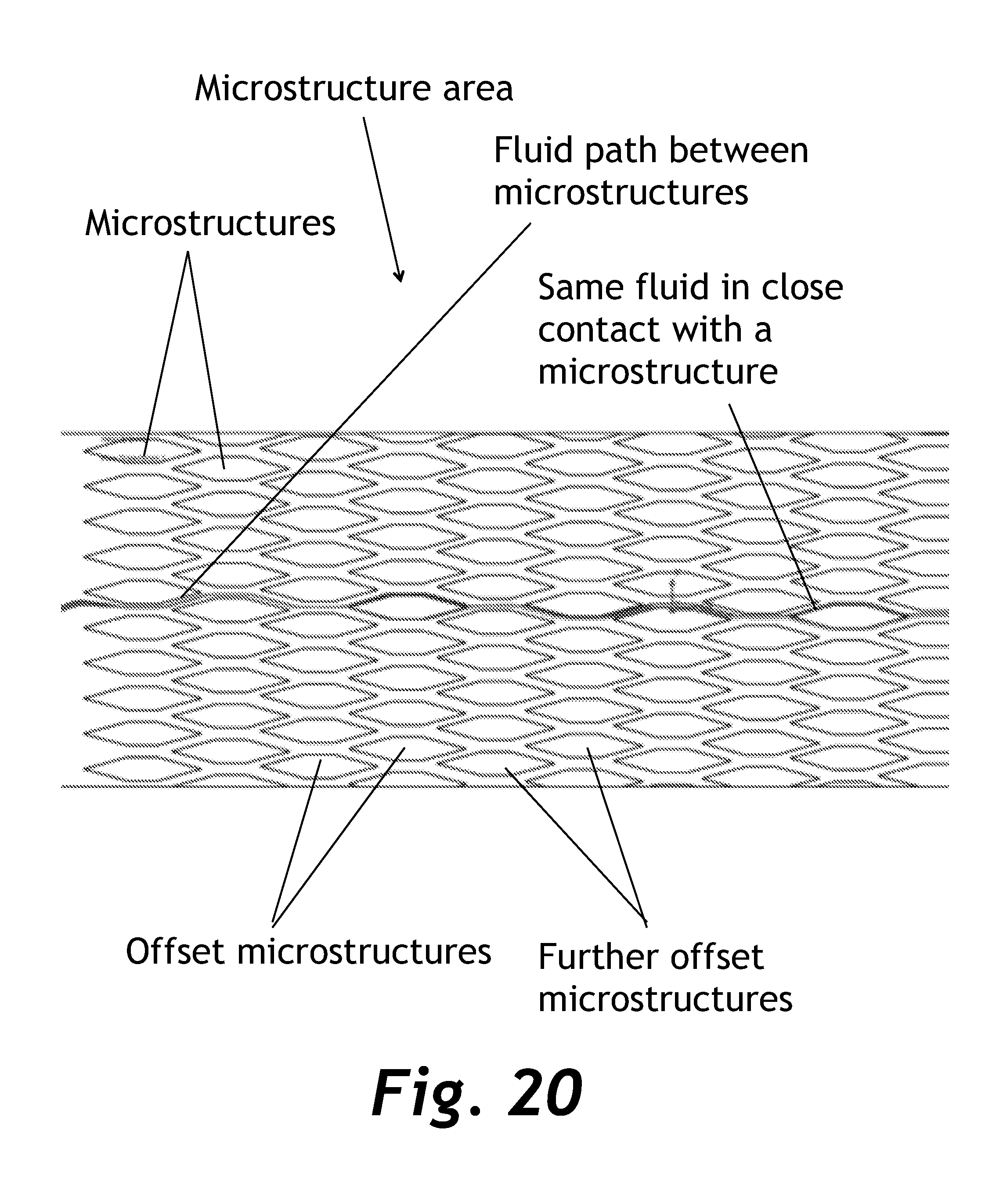
[0026] FIG. 20 is a close-up view of an alternate embodiment of the microstructure area of the filter panel shown in FIG. 4 that includes fluid flow lines.
[0027] FIG. 21 is a close-up view of FIG. 20 with example dimensions.
[0028] FIG. 22 is a close-up front view of an alternate embodiment of the microstructure area shown in FIG. 4.
[0029] FIG. 23 is a perspective view of an example microstructure filter panel.
[0030] FIG. 24 is a close up perspective view of the microstructure filter panel of FIG. 23.
[0031] FIG. 25 is side perspective view of the microstructure filter panel of FIGS. 23-24.
[0032] FIG. 26 is a perspective view of a plurality of microstructure filter panels in stacked configuration.
[0033] FIG. 27 is a perspective view of an example microstructure filter device for use in a chromatograph device.
[0034] FIG. 28 is a cross section view of the example microstructure filter device of FIG. 27.
[0035] FIG. 29 is an end view of the microstructure filter device of FIG. 28.
[0036] FIG. 30 is a perspective view of a microstructure filter.
[0037] FIG. 31 is another perspective of the microstructure filter.
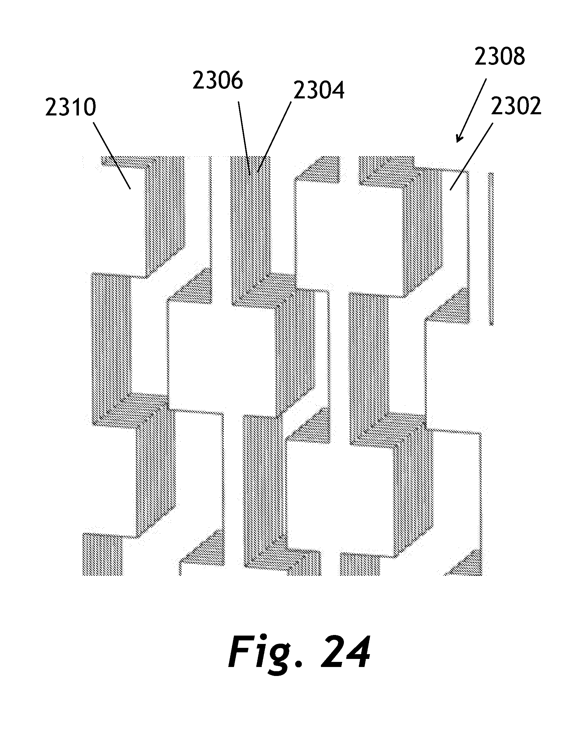
[0038] FIGS. 32A and 32B collectively illustrate spacers and openings of layers of the microstructure filter.
[0039] FIG. 33 illustrates nanoscale coatings applied to filter features of a microstructure filter device.
[0040] FIG. 34 is another example microstructure filter device.
[0041] FIG. 35 is a close up view of a first end of the microstructure filter device of FIG. 34.
[0042] FIG. 36 is an even closer view of the microstructure filter of the microstructure filter device of FIG. 34.
[0043] FIG. 37 is yet a closer view of FIG. 36.
[0044] FIG. 38 is a perspective view of an example microstructure filter device in a tubular configuration.
[0045] FIG. 39 illustrates the microstructure filter device of FIG. 38 in a cutaway view.
[0046] FIG. 40 is a perspective view of an example chromatograph device.
[0047] FIG. 41 is an exploded view of the chromatograph device illustrating a microstructure filter.
[0048] FIG. 42 is a view of a portion of the microstructure filter of the device of FIG. 40.
[0049] FIG. 43 is a closer view of the microstructure filter of FIG. 42.
[0050] FIGS. 44A and 44B illustrate additional perspective views of the microstructure filter.
[0051] FIG. 45 is a perspective view of the microstructure filter showing channels and bars.
[0052] FIG. 46 is a perspective view of the microstructure filter showing spacer (structural) material.
[0053] FIG. 47 illustrates a cutaway section showing filter features with nanoscale coatings.
[0054] FIG. 48 illustrates a top down view of layers of the microstructure filter, showing offsetting of layers.
[0055] FIG. 49 illustrates a process of photoresist, deposition, and etching to create a microstructure filter.
[0056] FIG. 50 illustrates a frit in combination with a chromatograph connector.
[0057] FIGS. 51 and 52 collectively illustrate perspective views of the frit, showing passages.
[0058] FIGS. 53 and 54 illustrate a front elevational view of an example disk shaped microstructure filter device.
[0059] FIGS. 55-59 illustrate close up views of a microstructure filter of the microstructure filter device of FIGS. 53-54.
[0060] FIG. 60 illustrates another detail section of the microstructure filter of the microstructure filter device.
[0061] FIG. 61 illustrates a front elevational view of an example disk shaped microstructure filter device with a layered configuration.
[0062] FIG. 62 is a close up perspective view of the filter features of the microstructure filter of the microstructure filter device.
[0063] FIGS. 63-65 collective illustrate a process for creating thin bars which form the filter features of the microstructure filter.
DESCRIPTION OF EXEMPLARY EMBODIMENTS
[0064] While this technology is susceptible of embodiment in many different forms, there is shown in the drawings and will herein be described in detail several specific embodiments with the understanding that the present disclosure is to be considered as an exemplification of the principles of the technology and is not intended to limit the technology to the embodiments illustrated.
[0065] The terminology used herein is for the purpose of describing particular embodiments only and is not intended to be limiting of the present technology. As used herein, the singular forms "a", "an" and "the" are intended to include the plural forms as well, unless the context clearly indicates otherwise. It will be further understood that the terms "comprises" and/or "comprising," when used in this specification, specify the presence of stated features, integers, steps, operations, elements, and/or components, but do not preclude the presence or addition of one or more other features, integers, steps, operations, elements, components, and/or groups thereof.
[0066] It will be understood that like or analogous elements and/or components, referred to herein, may be identified throughout the drawings with like reference characters. It will be further understood that several of the figures are merely schematic representations of the present technology. As such, some of the components may have been distorted from their actual scale for pictorial clarity.
[0067] FIGS. 1-22 collectively illustrate separation filters with microstructured panels. The microstructured panels are precisely replicated on a film from tooling made with semiconductor processing techniques. The separation panels can be covered with a front cover or layered on top of one another to form enclosed panels. The flow of liquids through the microstructured panels can be affected by coating the surfaces of the panels with materials or be constructed of materials that attract or repel particles or molecules in the fluid. Alternately separation panels can be made from semiconductor materials rather than being replicated from a semiconductor master.
[0068] Referring first to FIG. 1, the separation filter is shown. Fluids flow into the separation filter at the inlet tube. The opening in the inlet tube extends through the front plate. Fluids exiting the separation filter do so via the outlet tube. The opening in the outlet tube also extends through the front plate. The filter panel is sealed to the back side of the front plate. The back side of the front panel would be generally a flat surface and is not shown.
[0069] Referring to FIG. 2 the filter panel is shown without the inlet tube, the outlet tube and the front cover. The inlet area is coincident with the opening in the inlet tube. Similarly the outlet area is coincident with the opening in the outlet tube. The inlet area is a recessed pocket in the filter panel. Fluids flow from the inlet area to the inlet expansion area. The inlet expansion area is also a recessed pocket in the separation panel.
[0070] The cross section of the inlet expansion area is shown to increase along the flow path. The amount of expansion, or contraction would be a parameter that would be engineered for the specific application of the separation filter. The depth of the expansion is shown to be constant. This does not necessarily need to be the case.
[0071] The inlet expansion area is connected to the microstructure area. FIGS. 2, 3, 4 and 5 show the microstructure area at various angles and level of detail. The microstructure area shares the same depth as the inlet area and the inlet expansion area. Microstructures are generally as tall as the depth of the pocket.
[0072] As mentioned above the surface coating of the microstructure panel or the material composition of the microstructure panel would be of a type that interacts with compounds in the fluid. The removal of chemicals and or particles from drinking water is one applications of the disclosed separation filter. With this type of filter it is desirable to retain chemicals or particles from the fluid.
[0073] Another application of the separation panel is chromatography. When used in chromatography different compounds are usually separated from one another at different rates as fluid flows through the separation filter.
[0074] It should be noted that the coating and or materials deployed with the filter used for the specific separation task of the filter is not part of this invention. One skilled in the art of separation filters and the materials used for the specific application could engineer a material for a specific fluid.
[0075] Referring to FIG. 5 the microstructures can be seen in a magnified isometric view. The microstructures are generally a diamond shaped cross section and extend from the pocketed surface of the separation panel to the front face of the separation panel. This particular embodiment has a constant cross section from the base to the front face. The diamond microstructure geometry generally results in a constant cross section of the fluid path through the microstructure area.
[0076] Referring to FIG. 6, flow lines of a fluid flowing around the microstructures is shown. These flow lines were generated with a computational fluids dynamics analysis. It should be noted that for most applications of the disclosed type filter the flow would be laminar in type.
[0077] As fluid flows along the surface of the microstructures, a boundary layer develops and grows in thickness. The fluid making contact with the surface of the filter microstructures is essentially stationary in relationship to the fluid flowing midway between adjacent microstructures. The further the fluid is from the surface of a microstructure the less likely a particle will be attracted to the surface of the microstructure.
[0078] The midway point is where the fluid velocity is greatest. This higher velocity fluid strikes the tips of the next column of microstructures. The boundary layer that begins to form at the tip of the next column of microstructures was previously the furthest away from the surface of the 1.sup.st column of microstructures.
[0079] Referring to FIG. 7 where an alternate embodiment of the microstructure is shown. These microstructures are also arranged to split the flow path as with the diamond design.
[0080] Referring to FIG. 8 where another alternate embodiment of the microstructure is shown. The microstructures are tapered along the flow path to compensate for the growth of the boundary layers.
[0081] Referring to FIGS. 9, 10, 11, 12 and 13 where another alternate embodiment of the microstructure is shown. These microstructures differ from the previously disclosed microstructures in that they do not have a constant cross section. These microstructures have small spacers (in cross section) located between larger thin planes of structural material. This embodiment yields more surface area per section separation filter panel. Panels of this type require a more complex manufacturing process.
[0082] Referring to FIG. 14, the process to fabricate these microstructures is described.
[0083] Referring to FIG. 15, additional "plumbing" has been added to the separation panel. Channels to and from a sensing area are shown. These additional features could be added to any of the embodiments disclosed in this disclosure. The sensing area could be used to measure the optical transmission or reflection of the fluid as it exits the separation filter. This would be useful in the case where the separation filter was used for chromatography.
[0084] Referring to FIG. 16, two different micro structured areas and two sensing areas are combined in series along the flow path. The first microstructure area might be coated with a different material than the second area.
[0085] Referring to FIG. 17 where another alternate embodiment of a separation filter is shown. The separation filter is configured with many through hole filter panels sandwiched between the front panel and the rear panel.
[0086] Referring to FIG. 18, the through hole filter panel is shown. The inlet area of the through hole filter panels pass all the way through the panel. This allows inlet and outlet fluids to flow to all of the panels in the sandwich. The rear panel doesn't have any holes.
[0087] Referring to FIG. 19, an alternate embodiment of the filter panel with vertically offset inlet and outlet areas is shown. This geometry yields flow paths that are more common in length than disclosed in previous Figs.
[0088] Referring to FIG. 20, an alternate embodiment of the filter panel is shown with slight vertical offsets in the vertical height of the microstructures in the microstructure area. By slightly offsetting the height of the microstructures the tip of the microstructure cut through slightly different points in the flow path. Without the offset the same cross sections of flow would contact the surface of the microstructures over and over as the flow progresses through them.
[0089] The flow lines are only shown for one elevation of the fluid flow. Flow through a separation filter of this type would likely be one with a low Reynolds number. Low Reynolds number flows result in a laminar type boundary layer.
[0090] The first column cuts the flow stream at specific heights. These heights can accurately be located when the microstructures are fabricated directly from semiconductor type processes or if they are replicated from a tool made from semiconductor processes. The second column of microstructures cuts the flow field directly in the center of the flow between the microstructures in the first column.
[0091] The third column is off slightly vertically from the first column. The fluid cut by the third column of microstructures is cut slightly above the path cut by the first column of microstructures. One would want to design this vertical offset while considering the flow rate and attractive force between the particles or compound in the fluid and the surface of the microstructure.
[0092] Successive columns of microstructures would be offset by the same amount. With only a relatively small number of offset microstructures one could insure that all areas of the flow path pass within close proximity to the surface of a microstructure.
[0093] Example dimensions of the embodiment shown in FIG. 20 are shown in FIG. 21. The design is shown with a 20 .mu.m space between all of the microstructures. The third column of microstructures is offset vertically upwards from the first column of microstructures by 2 .mu.m. Fluid flowing 2 .mu.m above the center of the first column of microstructures would eventually be cut in half by the tip of a microstructure in the third column. Fluid flowing 4 .mu.m above the center of the first column of microstructures would be cut in half by the tip of s microstructure in the fifth column of microstructures. To cut the fluid flow at every 2 .mu.m interval it would require a total of 20 columns of microstructures. To cut the fluid flow at every 1 .mu.m interval it would require twice as many columns of microstructures. By varying the offset of pairs of columns a system can be designed for efficient separation of particles or compounds from a fluid. It should be noted that for a column offset of 2 .mu.m a particle is no more than 1 .mu.m away from a surface. It would be less than 1 .mu.m above or greater than 1 m below the surface of a microstructure. It should be further noted that laminar flow of the fluid is required, if the flow was to become turbulent the alignment of cuts would be disturbed.
[0094] It should be noted that these values are given to describe the geometric advantages of 3D microstructure filter technology. Those knowledgeable in fluid chemistry would want to engineer the structure for the specific fluids, particles, microstructure surface materials and flow rates.
[0095] The microstructures shown are ones consistent with ones made with semiconductor processes or replicated from them. These manufacturing techniques consistently produce features of a depth of 10 times the width. Following this guideline the microstructures could be 300 um deep. The entire cross section of the flow field would then be 0.15 sq. mm. The length of the flow microstructures would only need to be 2 mm long for a cut interval of 2 .mu.m. For a 1 um cut interval the length would be 4 mm long. For a 4 mm length the total volume of the microstructure volume would be only 0.6 cubic mm or 0.6 Cpl. Because of this tiny volume only a small sample size is require. Further, because of the short path length, the pressure to move fluid through the microstructures would be relatively small. A further advantage is that all of the flow paths are equal in length and cross section. This common path length equates to consistent attraction of particles along the flow path. If it is desirable to have a greater amount of fluid filters panels could be laminated together as shown in FIG. 17.
[0096] Referring to FIG. 22 an alternate embodiment of the filter panel is shown with microstructures that are truncated at the trailing end. The truncation disrupts and generally mixes the flow to mix the flow vertically. Mixed flow increases the likelihood that all areas of the flow path will come in close proximity to the surface of at least one microstructure. This embodiment is less desirable that the previously described embodiment but would still produce reasonable performance.
[0097] The present technology is directed to separation, and more specifically, but not by way of limitation, to separation mechanisms that comprise multiple microstructures made from or coated with materials commonly used in separation. Some of these materials are mentioned in the prior art section. These separation microstructure panels are configured to maximize separation of the compounds within the fluid. The separation filter may be used in chromatography or reverse type chromatography.
[0098] FIG. 23 illustrates an example multilayer microstructure filter panel 2300. The panel 2300 is illustrated in greater detail in FIGS. 24 and 25. A close up view of a section of the panel 2300 is illustrated in FIG. 24 while a cross sectional view of a second of the filter panel 2300 is illustrated in FIG. 25. The panel 2300 is comprised of a base material 2302, also referred to as a wafer. A plurality of alternating structural and sacrificial layers (such as structural layer 2304 and sacrificial layer 2306) are disposed on the base material 2302. An example process for creating layered structures is described in greater detail above. Also, additional aspects of microstructure filter creation are found in applicant's co-pending U.S. patent application Ser. No. X, filed on X, which is hereby incorporated by reference here in its entirety, including all references cited therein.
[0099] The alternating structural and sacrificial layers are etched to create input and output channels, such as input channel 2308 and output channel 2310. When portions of the sacrificial layers are removed openings (e.g., holes, slits, cuts, slots, etc.) between the input channel 2308 and output channel 2310 are created, which allow for cross flow of fluid therebetween. The size of the openings functions to remove particles from the fluid. In some embodiments, rather than having openings, the sacrificial material can be comprised of a porous material that filters the fluid.
[0100] In some embodiments, the panel 2300 comprises an outer layer 2312, which can comprise a photoresist layer. In one embodiment, each of the structural layers is approximately 75 nanometers in height, while each of the sacrificial layers is approximately 15 nanometers high. The outer layer 2312 can have a height of approximately 1.5 microns. As mentioned before, the sacrificial layers can be partially etched to create perforations or openings.
[0101] Referring to FIG. 26, which illustrates a plurality of multilayer microstructure filter panels stacked together. As illustrated, fluid 2602 enters the input channels, such as input channels 2604 and 2606, and passes through regions of cross channels 2608 and 2610 and ultimately out of output channels such as output channels 2612 and 2614.
[0102] To be sure, the multilayer microstructure filter panels and stacks of multilayer microstructure filter panels can be utilized to manufacture various filtering devices as well as chromatograph devices, as will be described in greater detail below.
[0103] FIG. 27 illustrates another example filter device 2800 constructed from a plurality of multilayer microstructure filter panels. The panel comprises a base housing 2802 that holds a plurality of multilayer microstructure filter panels. The base housing 2802 can be manufactured from a glass or silicon material, as well as from other materials that would be known to one of ordinary skill in the art with the present disclosure before them. The device 2800 is configured to filter a fluid 2801 entering one end of the device 2800 and exiting a terminal opposite end of the device 2800 exiting a terminal opposite end of the device 2800.
[0104] The details of the plurality of multilayer microstructure filter panels are illustrated in greater detail in FIGS. 27-32B. FIG. 28 is a cross sectional view of the filter device 2800 of FIG. 27. The microstructure filter panel 2804 comprises an inlet 2803 and an outlet 2805. The inlet and outlet can be created through etching or other similar processes.
[0105] FIG. 29 is an end view of the device 2800 illustrating a multilayer microstructure filter panel 2804 nested within the base housing 2802. FIG. 30 illustrates various spacer layers (structural layers), such as structural layer 2806. A series of structural and sacrificial layers comprise the microstructure filter panel 2804. In one embodiment, the microstructure filter panel 2804 is etched to expose a plurality of layered sections, such as layered section 2808.
[0106] FIG. 31 is a close up perspective view of a structure layer section of the microstructure filter panel 2804. The structure layer section illustrates various layers of structural layers, such as structural layer 2810 and sacrificial layer 2812. A series of spacers such as spacer 2810 can be comprised of sacrificial material.
[0107] FIGS. 32A and 32B collectively illustrate additional perspective views of the microstructure filter panel 2804 showing the layering and openings created within the microstructure filter panel 2804. The microstructure filter panel 2804 is illustrated with spacers of sacrificial material 2812, structural layers 2806, and sacrificial layer sections which are partially removed (or entirely) to create openings 2814 through which fluid can flow.
[0108] In some embodiments, an effective surface area or fluidic surface area of the microstructure filter panels, such as the cross channels can be increased by creating nanoscale structures or other texturing on the surfaces. For example, FIG. 33 is a close up view of a cross channel section 3402 which is provided with a nanoscale coating 3404. The nanoscale coating 3404 can be created through a depositing process or by etching away of sacrificial material.
[0109] It will be understood that one of ordinary skill in the art with the present disclosure before them would be capable of using other conventional coating processes for creating three dimensional features on the surfaces of the microstructure filter panels.
[0110] The three dimensional nature of the microstructure filter panels, whether including nanoscale cladding or not, provides a five-fold increase in particulate attraction forces compared with filter devices of lower dimensions.
[0111] FIG. 34 illustrates another example filter device 3500. The device 3500 also comprises a base housing 3502 that can be manufactured from a glass or silicon material, as well as from other materials that would be known to one of ordinary skill in the art with the present disclosure before them. The base housing 3502 is configured with an inlet notch 3504 (a close view illustrated in FIG. 35) and an outlet notch 3506. In some embodiments, a portion of the inlet notch 3504 is angled relative to a reference line X. In some embodiments, a portion of the outlet notch 3506 is also angled relative to the reference line X. In one embodiment the inlet notch 3504 angles upwardly as it extends from a first end of the base housing 3502 and the outlet notch 3506 angles from a narrow portion to a second end of the base housing 3502 that is opposite the first end.
[0112] A plurality of multilayer microstructure filter panels is combined to create a microstructure filter 3508 is disposed at an angle .theta. relative to the reference line X. The filter panel 3508 extends between the inlet notch 3504 and the outlet notch 3506.
[0113] Fluid will enter the inlet notch 3504 and be dispersed into the microstructure filter 3508. The fluid passes through the microstructure filter panel 3508 into the outlet notch 3506. To be sure, fluid can enter the microstructure filter 3508 along the length of the inlet notch 3504 and exit the microstructure filter 3508 along the length of the outlet notch 3506.
[0114] FIG. 36 illustrates a close view of a portion of the microstructure filter 3508. A plurality of layered sections, such as layered section 3510 is illustrated, as well as a plurality of structure/support sections 3512. Again, the layered sections can be comprised of layers of structural and sacrificial materials.
[0115] FIG. 37 illustrates an even closer view of portion of the microstructure filter 3508 presented in FIG. 36. The layered section 3510 is comprised of a series of channels and sidewalls 3514 that filter the fluid as it passes through the microstructure filter 3508. Each of the layers can comprise channels and sidewalls of different thicknesses. For example, channels and sidewalls disposed near the inlet notch 3504 can be sized to attract particles larger than the particles attract by the channels and sidewalls proximate the outlet notch 3506 (FIG. 34).
[0116] FIG. 38 is an example filtering device 3900 that is constructed in accordance with the present technology. The filtering device 3900 includes a tubular housing 3902 that comprises an input port 3904 and an output port (not shown), which is identical to the input port 3904 but disposed on an opposing end of the filtering device 3900.
[0117] FIG. 39 illustrates that the example filter device 3500 of FIGS. 34-37 is utilized in the filtering device 3900. That is, the housing 3902 is configured to receive the example filter device 3500. The filter device 3500 can be used to filter any fluid for any number of applications.
[0118] FIG. 40 illustrates an exemplary filter device 4100 in the form of a testing column. The device 4100 comprises a housing 4102 having fittings 4104 and 4106. In some embodiments, the housing 4102 is separable into a first section 4108 and a second section 4110 as illustrated in FIG. 41. The device 4100 comprises a microstructure filter 4112. The second section 4110 operates as a cover that bounds the uppermost (or outermost) layer of the microstructure filter 4112, ensuring that fluid transits through the microstructure filter 4112. An input tube 4101 transmits fluid from the fitting 4104 to the microstructure filter 4112.
[0119] FIG. 42 illustrates the microstructure filter 4112 in more detail. The microstructure filter 4112 comprises an inlet 4114 and outlet 4116. In some embodiments, the inlet and outlet are each approximately one millimeter wide. The microstructure filter 4112 has layered sections 4120 and support sections 4122. The microstructure filter 4112 is illustrated in FIG. 43 as having a plurality of layered sections 4120A, 4120B, and 4120C that are slightly offset from one another. For example, structural features 4124 of layered section 4120B are positioned slightly higher than structural features 4126 of layered section 4120C. Cross channels such as cross channels 4128 have a height that is approximately 50 micrometers and the width of the layered sections are approximately 32 micrometers. In some embodiments, a pitch between individual cross channel features is ten micrometers.
[0120] FIGS. 44A and 44B are close up views of the microstructure filter 4112.
[0121] FIG. 45 is a close up view of a layered section of the microstructure filter 4112 illustrating channels, such as channels 4130 formed into layered sections (also referred to as "bars") through etching.
[0122] In some embodiments, a spacer material 4132 is utilized to maintain spacing of the layered sections as illustrated in FIG. 46.
[0123] FIG. 47 illustrates that the individual structural layers of the layered sections (e.g., 4120A-C) can be coated or manufactured with three dimensional coatings 4134. This again increases the surface area of the layered sections, which improves the filtering capabilities of the microstructure filter 4112. Again, one of ordinary skill in the art could use various coating processes to coat the individual structural layers to create artifacts that result in the creation of three dimensional aspects on the structural layers.
[0124] FIG. 48 is a top down view of the microstructure filter 4112 taken across section view A-A. The layered sections are shown as comprising individual cross channel filter features, such as filter features 4136. Again, filter features 4136 of adjacent layered sections can be offset from one another, which allow the fluid to be flowing close to a surface of a structural layer ensuring that the fluid contacts at least one surface.
[0125] In some embodiments, the features of the structural layers can be staggered or offset from one another by approximately one nano-meter or any other distance per design requirements. Offsetting of structural layers causes the fluid 4138 to divert downwardly from filter features 4136 to adjacent filter features 4140. Also, offsetting of the layers and resulting features reduces and/or eliminates the effect of accelerating of the fluid as would commonly occur through a straight-line channel or path. The same effect is produced in device of FIG. 21.
[0126] FIG. 49 illustrates the creation of a microstructure filter which begins with a step S002 of photolithography and deposition of a sacrificial layer. Sections of sacrificial material are spaced apart from one another. Step S004 includes the photolithography and deposition of another sacrificial layer that is offset from the sacrificial layer in step S002. Pairs of sections of the second sacrificial layer are placed on the first sections of the sacrificial layer such that half of the sections of the first layer are visible.
[0127] In step S006 photolithography and deposition of a third sacrificial layer, which is illustrated as being offset from the second sacrificial layer in step S004. Triplet sections of sacrificial layers overlap the sections of the second and first sacrificial layers.
[0128] In step S008 photolithography and deposition of a fourth sacrificial layer is illustrated. The fourth layer is deposited on the third layer in continuous sections, covering approximately half of the microstructure filter. Next, in step S010 structural layers are deposited over the sacrificial layers so as to create a covering. The device is then etched in step S112 to create openings, such as opening 5114.
[0129] In sum, with a series of photolithography, deposition, and etch processes, staggered bars can be created. With four "digital" layers 16 steps can be created and the layers can be staggered incrementally at a distance of one nanometer or less.
[0130] FIG. 50 illustrates an exemplary filter device connector 5100 that comprises a frit 5102. The frit 5102 is placed into the body of the connector in a path of fluid communication 5104. The frit 5102 can retain particles as well as ensure that longitudinal dispersion of these particles through the filter device is also reduced. To be sure, the filter device connector 5100 can be utilized as the fitting 4104 of FIG. 40.
[0131] The frit 5102 comprises a diameter D and a thickness as illustrated.
[0132] FIGS. 51 and 52 collectively illustrate an example frit 5102 that comprises an outer peripheral sidewall 5106 that encircles a plurality of sections of passages. For example, the frit 5102 can include sections 5108A-E, which are each disposed in ringed configurations. In some embodiments the sections are arranged into hexagonal shapes of passages, although other shapes are likewise contemplated for use.
[0133] In some embodiments, each section moving progressively outward will be sized to capture a different size of particle. For example, section 5108A has passages that are the smallest in diameter, while section 5108E has passages that are largest in diameter. Sections in between 5108A and 5108E have progressively larger passages than the section which they encompass. In some embodiments, each section can have a unique size of passages and these sections need not be arranged in a linear manner with respect to passage size.
[0134] In some embodiments, not only the diameter of the passages can be varied but also the spacing of the passages. The density of the passages can be tailored to design requirements for operation of the device.
[0135] FIGS. 53-65 collectively illustrate further examples of microstructure filters that can be utilized in the devices of the present disclosure. In general, these microstructure filters can comprise disks with microstructures (e.g., filter features) that filter either particles or solutes from fluids. A top surface of the disk would typically be mated to a flat surface to enclose the flow channels on the micro structured disk. In some embodiments, layers of disks can be stacked on top of one another. The disks can be configured in parallel or in series configurations.
[0136] As with other microstructure filters, these disks can be coated with different materials to filter different solutes in the fluid. These coatings can include nanoscale structures. Disks with different coatings can be configured in either in series or parallel configurations as well. In some embodiments, the structures can be coated with copper, zinc, carbon, resins and SiO2 are some materials, although many other coatings could be used.
[0137] FIG. 53 illustrates a microstructure filter 5400 in disk shape. The filter 5400 comprises a plurality of inlet channels, such as inlet channels 5402 that deliver fluid to a plurality of horizontal channels, such as horizontal channels 5404. The filter 5400 also comprises outlet channels 5406 that collect fluid from the horizontal channels. To be sure the inlet and outlet channels can be switched relative to their configurations such that the outlet channels become inlet channels and vice versa.
[0138] FIG. 54 illustrates two detail sections 5408 and 5410 that will be described in greater detail herein. In FIGS. 55-59 illustrate filter features of the detail section 5408. For example, in FIG. 55, both large and small flow channels are illustrated. An inlet channel 5412 is illustrated, which feeds fluid to inlet horizontal channels 5416 and outlet horizontal channels 5418. An outlet channel 5420 collects filtered fluid from the inlet horizontal channels 5416 and outlet horizontal channels 5418.
[0139] FIG. 56 illustrates horizontal channels with post filter features 5422. Other filter features such as slits, notches, and grooves of varying size and shape can be utilized as well.
[0140] FIG. 57 illustrates a top down view of the inlet horizontal channels 5416 and outlet horizontal channels 5418.
[0141] FIG. 58 illustrates a top down view of the inlet horizontal channels 5416 and outlet horizontal channels 5418 with post filter features, and FIG. 59 is a close up view of a section of the view of FIG. 58.
[0142] FIG. 60 illustrates detail section 5410 in more detail. The detail section includes a vertical outlet channel 5424, horizontal inlet channels 5416, and an outlet port 5418. In some embodiments, the vertical outlet channel 5424, horizontal inlet channels 5416, and support layers are coplanar with one another.
[0143] FIG. 61 illustrates another microstructure filter 6200 in disk shape with a layered design. A more detailed view of filter features 6202 of the filter 6200 is illustrated in FIG. 62. The filter features comprise sidewalls instead of posts. In FIG. 64 a more detailed view of the sidewalls is provided. In some embodiments, the walls can be 0.1 nanometers tall and 0.05 nanometers wide.
[0144] FIGS. 63-65 illustrate a layer deposition process for creating the sidewalls. In FIG. 63, thin bars 6402 are printed or coated onto a support surface 6404. The material used in this deposition process can be a sacrificial material. A second layer 6406 is deposited onto the bars 6402 and can be created from a structural material.
[0145] Additional bars of structural and/or sacrificial material can be applied to the bars 6402 as illustrated FIG. 64.
[0146] A view of a section of a completed filter disk is illustrated in FIG. 65. To be sure, when sacrificial layers are removed filter orifices 6602 (filter features) are created. Again, the surface of these bars and surfaces can be coated as needed.
[0147] While various embodiments have been described above, it should be understood that they have been presented by way of example only, and not limitation. The descriptions are not intended to limit the scope of the technology to the particular forms set forth herein. Thus, the breadth and scope of a preferred embodiment should not be limited by any of the above-described exemplary embodiments. It should be understood that the above description is illustrative and not restrictive. To the contrary, the present descriptions are intended to cover such alternatives, modifications, and equivalents as may be included within the spirit and scope of the technology as defined by the appended claims and otherwise appreciated by one of ordinary skill in the art. The scope of the technology should, therefore, be determined not with reference to the above description, but instead should be determined with reference to the appended claims along with their full scope of equivalents.
* * * * *
D00000
D00001
D00002
D00003
D00004
D00005
D00006
D00007
D00008
D00009
D00010
D00011
D00012

D00013

D00014

D00015

D00016

D00017

D00018

D00019

D00020
D00021

D00022

D00023

D00024
D00025

D00026

D00027

D00028

D00029

D00030

D00031

D00032

D00033

D00034

D00035

D00036

D00037

D00038

D00039

D00040

D00041

D00042

D00043

D00044

D00045

D00046

D00047

D00048

D00049

D00050

D00051

D00052

D00053

D00054

D00055

D00056

D00057

D00058

D00059

D00060

D00061

D00062

D00063

D00064

D00065

XML
uspto.report is an independent third-party trademark research tool that is not affiliated, endorsed, or sponsored by the United States Patent and Trademark Office (USPTO) or any other governmental organization. The information provided by uspto.report is based on publicly available data at the time of writing and is intended for informational purposes only.
While we strive to provide accurate and up-to-date information, we do not guarantee the accuracy, completeness, reliability, or suitability of the information displayed on this site. The use of this site is at your own risk. Any reliance you place on such information is therefore strictly at your own risk.
All official trademark data, including owner information, should be verified by visiting the official USPTO website at www.uspto.gov. This site is not intended to replace professional legal advice and should not be used as a substitute for consulting with a legal professional who is knowledgeable about trademark law.