Bonding Method
TAI; Tomoyoshi ; et al.
U.S. patent application number 16/135689 was filed with the patent office on 2019-01-31 for bonding method. The applicant listed for this patent is NGK INSULATORS, LTD.. Invention is credited to Keiichiro ASAI, Masashi GOTO, Yuji HORI, Masahiko NAMERIKAWA, Tomoyoshi TAI, Takashi YOSHINO.
| Application Number | 20190036009 16/135689 |
| Document ID | / |
| Family ID | 59901176 |
| Filed Date | 2019-01-31 |


View All Diagrams
| United States Patent Application | 20190036009 |
| Kind Code | A1 |
| TAI; Tomoyoshi ; et al. | January 31, 2019 |
BONDING METHOD
Abstract
A bonding layer 3 is formed over a piezoelectric material substrate, and the bonding layer 3 is made of or more material selected from the group consisting of silicon nitride, aluminum nitride, alumina, tantalum pentoxide, mullite, niobium pentoxide and titanium oxide. Neutralized beam A is irradiated onto a surface 4 of the bonding layer and a surface of a supporting body to activate the surface of the bonding layer and the surface of the supporting body. The surface of the bonding layer and the surface of the supporting body are bonded by direct bonding.
| Inventors: | TAI; Tomoyoshi; (Inazawa-City, JP) ; HORI; Yuji; (Owariasahi-City, JP) ; ASAI; Keiichiro; (Nagoya-City, JP) ; YOSHINO; Takashi; (Ama-City, JP) ; GOTO; Masashi; (Nagoya-City, JP) ; NAMERIKAWA; Masahiko; (Seto-City, JP) | ||||||||||
| Applicant: |
|
||||||||||
|---|---|---|---|---|---|---|---|---|---|---|---|
| Family ID: | 59901176 | ||||||||||
| Appl. No.: | 16/135689 | ||||||||||
| Filed: | September 19, 2018 |
Related U.S. Patent Documents
| Application Number | Filing Date | Patent Number | ||
|---|---|---|---|---|
| PCT/JP2017/006461 | Feb 22, 2017 | |||
| 16135689 | ||||
| Current U.S. Class: | 1/1 |
| Current CPC Class: | H01L 41/39 20130101; H03H 9/02559 20130101; H03H 3/08 20130101; H01L 41/337 20130101; H03H 9/02228 20130101; H01L 41/1873 20130101; H03H 9/02834 20130101; H03H 9/17 20130101; H03H 9/02574 20130101; H01L 41/1871 20130101; H03H 9/02866 20130101; H03H 9/25 20130101; H03H 3/10 20130101; H01L 41/313 20130101; H03H 9/0585 20130101; H03H 9/145 20130101; H03H 9/02826 20130101 |
| International Class: | H01L 41/313 20060101 H01L041/313; H03H 9/145 20060101 H03H009/145; H03H 9/02 20060101 H03H009/02; H03H 9/25 20060101 H03H009/25; H03H 3/08 20060101 H03H003/08; H03H 9/05 20060101 H03H009/05; H03H 9/17 20060101 H03H009/17; H01L 41/187 20060101 H01L041/187; H01L 41/337 20060101 H01L041/337; H01L 41/39 20060101 H01L041/39 |
Foreign Application Data
| Date | Code | Application Number |
|---|---|---|
| Mar 25, 2016 | JP | 2016-061710 |
Claims
1. A method of bonding a piezoelectric material substrate and a supporting body comprising a single crystal, said method comprising the steps of: providing a silicon oxide film on said piezoelectric material substrate; forming a bonding layer on said silicon oxide film, said bonding layer comprising one or more material selected from the group consisting of silicon nitride, aluminum nitride, alumina, tantalum pentoxide, mullite, niobium pentoxide and titanium oxide; irradiating a neutralized beam onto a surface of said bonding layer and a surface of said supporting body to activate said surface of said bonding layer and said surface of said supporting body; and bonding said surface of said bonding layer and said surface of said supporting body by direct bonding.
2. The method of claim 1, further comprising the step of processing said piezoelectric material substrate to form a roughened surface, wherein said silicon oxide film and said bonding layer are provided on said roughened surface.
3. The method of claim 1, wherein said surface of said bonding layer is activated after said surface of said bonding layer is flattened.
4. The method of claim 1, wherein said supporting body comprises a material selected from the group consisting of silicon, sapphire and quartz.
5. The method of claim 1, wherein said piezoelectric material substrate comprises a piezoelectric single crystal.
6. The method of claim 5, wherein said piezoelectric single crystal comprises lithium niobate, lithium tantalate or lithium niobate-lithium tantalate solid solution.
7. A method of bonding a piezoelectric material substrate comprising a piezoelectric single crystal and a supporting body comprising a single crystal, said method comprising the steps of: providing a silicon oxide film on said supporting body; forming a bonding layer on said silicon oxide film, said bonding layer comprising one or more material selected from the group consisting of silicon nitride, aluminum nitride, alumina, tantalum pentoxide, mullite, niobium pentoxide and titanium oxide; irradiating a neutralized beam onto a surface of said bonding layer and a surface of said piezoelectric material substrate to activate said surface of said bonding layer and said surface of said piezoelectric material substrate; and bonding said surface of said bonding layer and said surface of said piezoelectric material substrate by direct bonding.
8. The method of claim 7, wherein said surface of said bonding layer is activated after said surface of said bonding layer is flattened.
9. The method of claim 7, wherein said supporting body comprises a material selected from the group consisting of silicon, sapphire and quartz.
10. The method of claim 7, wherein said piezoelectric single crystal comprises lithium niobate, lithium tantalate or lithium niobate-lithium tantalate solid solution.
11. A method of bonding a piezoelectric material substrate and a supporting body comprising a single crystal, said method comprising the steps of: forming a first bonding layer over said piezoelectric material substrate, said first bonding layer comprising one or more material selected from the group consisting of silicon nitride, aluminum nitride, alumina, tantalum pentoxide, mullite, niobium pentoxide and titanium oxide; forming a second bonding layer over said supporting body, said second bonding layer comprising one or more material selected from the group consisting of silicon nitride, aluminum nitride, alumina, tantalum pentoxide, mullite, niobium pentoxide and titanium oxide; irradiating a neutralized beam onto each of a surface of said first bonding layer and a surface of said second bonding layer to activate said surface of said first bonding layer and said surface of said second bonding layer; and bonding said surface of said first bonding layer and said surface of said second bonding layer by direct bonding.
12. The method of claim 11, further comprising the step of providing a silicon oxide film on said piezoelectric material substrate, wherein said first bonding layer is provided on said silicon oxide film.
13. The method of claim 11, further comprising the step of processing said piezoelectric material substrate to form a roughened surface, wherein said first bonding layer is provided on said roughened surface.
14. The method of claim 11, wherein said surface of said first bonding layer is activated after said surface of said first bonding layer is flattened.
15. The method of claim 11, further comprising the step of providing a silicon oxide film on said supporting body, wherein said second bonding layer is provided on said silicon oxide film.
16. The method of claim 11, wherein said surface of said second bonding layer is activated after said surface of said second bonding layer is flattened.
17. The method of claim 11, wherein said supporting body comprises a material selected from the group consisting of silicon, sapphire and quartz.
18. The method of claim 11, wherein said piezoelectric material substrate comprises a piezoelectric single crystal.
19. The method of claim 18, wherein said piezoelectric single crystal comprises lithium niobate, lithium tantalate or lithium niobate-lithium tantalate solid solution.
Description
CROSS-REFERENCE TO RELATED APPLICATIONS
[0001] This is a continuation of International Application No. PCT/JP2017/006461, filed Feb. 22, 2017, which claims priority of Japanese Patent Application No. 2016-061710, filed Mar. 25, 2016, the entire contents of which are incorporated herein by reference.
TECHNICAL FIELD
[0002] The present invention relates to a method of bonding a piezoelectric material substrate and a supporting body composed of a single crystal.
BACKGROUND ARTS
[0003] It is known a surface acoustic wave device functioning as a filter device or oscillator used in mobile phones or the like and an acoustic wave device such as lamb wave device or film bulk acoustic resonator (FBAR) using a piezoelectric thin film. As such acoustic wave device, it is known a device produced by adhering a supporting body and a piezoelectric substrate propagating a surface acoustic wave and by providing interdigitated electrodes capable of oscillating the surface acoustic wave on a surface of the piezoelectric substrate. By adhering the supporting body whose thermal expansion coefficient is lower than that of the piezoelectric substrate onto the piezoelectric substrate, the change of a size of the piezoelectric substrate responsive to temperature change is reduced so that the change of the frequency characteristics as the surface acoustic wave device is reduced.
[0004] For example, it is proposed, in patent document 1, a surface acoustic wave device having the structure produced by adhering a piezoelectric substrate and silicon substrate with an adhesive layer composed of an epoxy adhering agent.
[0005] Here, it is known that, in bonding a piezoelectric substrate and silicon substrate, a silicon oxide film is formed on a surface of the piezoelectric substrate, and a silicon substrate and the piezoelectric substrate are bonded through the silicon oxide film (patent document 2). In the bonding, plasma beam is irradiated onto the surfaces of the silicon oxide film and silicon substrate to activate the surfaces, followed by the direct boding (plasma activation method).
[0006] Further, it is known that a surface of the piezoelectric substrate is made a roughened surface, a filler layer is provided on the roughened surface to provide a flattened surface, and the filler layer is adhered onto a silicon substrate through an adhering layer (patent document 3). According to this method, an epoxy-based or acryl-based resin is used for the filler layer and adhering layer, and the bonding surface of the piezoelectric substrate is made the roughened surface to reduce the reflection of bulk wave and to reduce spurious wave. Further, as the adhesion is performed after the roughened surface is filled and flattened, air bubbles are hardly included in the adhering layer.
PRIOR ART DOCUMENTS
Patent Documents
[0007] (Patent document 1) Japanese Patent publication No. 2010-187373A [0008] (Patent document 2) U.S. Pat. No. 7,213,314 B2 [0009] (Patent document 3) Japanese Patent No. 5814727 B [0010] (Patent document 4) Japanese Patent publication No. 2014-086400A
SUMMARY OF THE INVENTION
Object to be Solved by Invention
[0011] In the case that a silicon substrate is directly bonded to a piezoelectric substrate, it is generally used plasma activation method. However, according to plasma activation method, hating is necessary for improving a strength after the bonding, and if the bonding temperature is low, the bonding strength tends to be lowered. However, as the bonding temperature is made high, cracks tend to occur due to a difference of the silicon substrate and piezoelectric substrate.
[0012] On the other hand, it is known a direct bonding method of so-called FAB (Fast Atom Beam) system (patent document 4). According to this method, neutralized atomic beam is irradiated onto the respective bonding surfaces at ambient temperature and the direct bonding is performed.
[0013] However, according to this method, the bonding strength of the silicon substrate and piezoelectric substrate is low, so that the separation may occur during the subsequent processing steps after the bonding.
[0014] An object of the present invention is, in directly bonding a piezoelectric material substrate and a supporting body composed of a single crystal, to enable the bonding at ambient temperature and to improve the bonding strength.
Means for Solving Object
[0015] First invention provides a method of bonding a piezoelectric material substrate and a supporting body comprising a single crystal, the method comprising the steps of:
[0016] forming a bonding layer over the piezoelectric material substrate, said bonding layer comprising one or more material selected from the group consisting of silicon nitride, aluminum nitride, alumina, tantalum pentoxide, mullite, niobium pentoxide and titanium oxide;
[0017] irradiating a neutralized beam onto a surface of the bonding layer and a surface of the supporting body to activate the surface of the bonding layer and the surface of the supporting body; and
[0018] bonding the surface of the bonding layer and the surface of the supporting body by direct bonding.
[0019] Second invention provides a method of bonding a piezoelectric material substrate comprising a piezoelectric single crystal and a supporting body comprising a single crystal, the method comprising the steps of:
[0020] forming a bonding layer over said supporting body, the bonding layer comprising one or more material selected from the group consisting of silicon nitride, aluminum nitride, alumina, tantalum pentoxide, mullite, niobium pentoxide and titanium oxide;
[0021] irradiating a neutralized beam onto a surface of the bonding layer and a surface of the piezoelectric material substrate to activate the surface of the bonding layer and the surface of the piezoelectric material substrate; and
[0022] bonding the surface of said bonding layer and the surface of the piezoelectric material substrate by direct bonding.
[0023] Third invention provides a method of bonding a piezoelectric material substrate and a supporting body comprising a single crystal, said method comprising the steps of:
[0024] forming a first bonding layer over the piezoelectric material substrate, the first bonding layer comprising one or more material selected from the group consisting of silicon nitride, aluminum nitride, alumina, tantalum pentoxide, mullite, niobium pentoxide and titanium oxide;
[0025] forming a second bonding layer over the supporting body, said second bonding layer comprising one or more material selected from the group consisting of silicon nitride, aluminum nitride, alumina, tantalum pentoxide, mullite, niobium pentoxide and titanium oxide;
[0026] irradiating a neutralized beam onto each of a surface of the first bonding layer and a surface of the second bonding layer to activate the surface of the first bonding layer and the surface of the second bonding layer; and
[0027] bonding the surface of the first bonding layer and the surface of the second bonding layer by direct bonding.
[0028] According to the present invention, when a piezoelectric material substrate and a supporting body composed of a single crystal are directly bonded, the bonding at ambient temperature can be realized and the bonding strength can be improved.
BRIEF DESCRIPTION OF THE DRAWINGS
[0029] FIG. 1(a) shows the state that a silicon oxide film 2 is provided on a piezoelectric material substrate 1, FIG. 1(b) shows the state that a bonding layer 3 is provided on the silicon oxide film 2, FIG. 1(c) shows the state that a surface 4a of a bonding layer 4 is subjected to flattening process, and FIG. 1(d) shows the state that a flat surface 4a is activated by neutralized beam A.
[0030] FIG. 2(a) shows the state that the piezoelectric material substrate 1 and supporting body 6 are bonded, FIG. 2 (b) shows the state that the piezoelectric material substrate 1 is thinned by processing, and FIG. 2(c) shows the state that electrodes 10 are provided on a piezoelectric material substrate 1A.
[0031] FIG. 3(a) shows the state that a surface of a piezoelectric material substrate 11 is made a roughened surface, FIG. 3(b) shows the state that a bonding layer 12 is provided on a roughened surface 11a, FIG. 3(c) shows the state that a surface 13a of a bonding layer 13 is subjected to flattening process, and FIG. 3(d) shows the state that a flat surface 14 is activated by neutralized beam A.
[0032] FIG. 4 (a) shows the state that a piezoelectric material substrate 11 and a supporting body 6 are bonded, FIG. 4(b) shows the state that the piezoelectric material substrate 11 is thinned by processing, and FIG. 4(c) shows the state that electrodes 10 are provided on a piezoelectric material substrate 11A.
[0033] FIG. 5(a) shows the state that a silicon oxide film 22 is provided on a roughened surface 11a of the piezoelectric substrate 11, a bonding layer 13A is provided on the silicon oxide film 22 and the bonding layer 13A is directly bonded to a surface 6a of the supporting body 6, FIG. 5(b) shows the state that the piezoelectric material substrate 11A is thinned, and FIG. 5(c) shows the state that electrodes 10 are provided on the piezoelectric material substrate 11A.
[0034] FIG. 6(a) shows the state that the silicon oxide film 2 and bonding layer 3 are provided on the supporting body 6, FIG. 6(b) shows the state that the surface 3a of the bonding layer 3 is subjected to flattening process, and FIG. 6(c) shows the state that the flat surface is activated by neutralized beam A.
[0035] FIG. 7(a) shows the state that the supporting body 6 and piezoelectric material substrate 1 are bonded, FIG. 7(b) shows the state that the piezoelectric material substrate 1A is further thinned by processing, and FIG. 7(c) shows the state that electrodes 10 are provided on the piezoelectric material substrate 1A.
[0036] FIG. 8(a) shows the state that the flat surfaces of the piezoelectric material layer 1 and of a first bonding layer 4A on the silicon oxide film 2 are activated, and FIG. 8(b) shows the state that a flat surface of a second bonding layer 4B on the supporting body 6 is activated.
[0037] FIG. 9(a) shows a bonded body of the piezoelectric material substrate 1 and supporting body 6, FIG. 9(b) shows the state that the piezoelectric material substrate 1A is thinned, and FIG. 9(c) shows the state that electrodes 10 are provided on the piezoelectric material substrate 1A.
[0038] FIG. 10(a) shows the state that a surface 14A of a first bonding layer 13A on the piezoelectric material substrate 11 is activated, and FIG. 10(b) shows the state that a flat surface 5B of a second bonding layer 4B on the supporting body 6 is activated.
[0039] FIG. 11(a) shows a bonded body of the piezoelectric material substrate 11 and supporting body 6, FIG. 11(b) shows the state that the piezoelectric material substrate 11A is thinned, and FIG. 11(c) shows the state that electrodes 10 are provided on the piezoelectric material substrate 11A.
[0040] FIG. 12(a) shows the state that the surface 14 of the first bonding layer 13A on the piezoelectric material substrate 11 is activated, and FIG. 12 (b) shows the state that a flat surface 5B of the second bonding layer 4B on the supporting body 6 is activated.
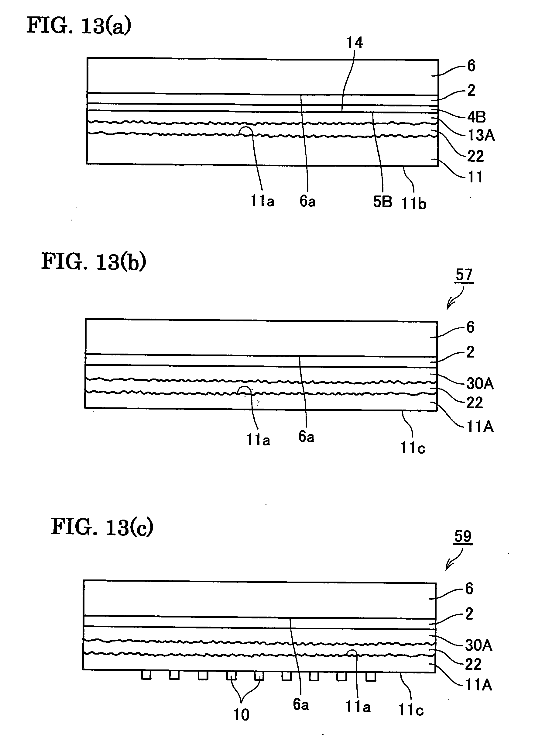
[0041] FIG. 13(a) shows a bonded body of the piezoelectric material substrate 11 and supporting body 6, FIG. 13(b) shows the state that the piezoelectric material substrate 11A is thinned, and FIG. 13(c) shows the state that electrodes 10 are provided on the piezoelectric material substrate 11A.
MODES FOR CARRYING OUT THE INVENTION
[0042] The present invention will be described in detail below, appropriately referring to the drawings.
[0043] FIGS. 1 to 5 relates to the first invention. Further, FIGS. 1 and 2 relates to an embodiment of providing a silicon oxide film on a piezoelectric material substrate.
[0044] As shown in FIG. 1(a), a silicon oxide film 2 is provided on a surface 1a of a piezoelectric material substrate 1. 1b represents a surface on the opposite side. Then, as shown in FIG. 1 (b), a bonding layer 3 is provided on the silicon oxide film 2. At this time, unevenness may be present on a surface of the bonding layer 3.
[0045] Then, according to a preferred embodiment, the surface 3a of the bonding layer 3 is subjected to flattening process to forma flat surface 4a. By this flattening process, a thickness of the bonding layer 3 is usually lowered to a thinner bonding layer 4 (refer to FIG. 1(c)). Then, neutralized beam is irradiated onto the flat surface 4a as an arrow A, as shown in FIG. 1(d), to activate the surface of the bonding layer 4A to obtain an activated surface 5.
[0046] On the other hand, as shown in FIG. 2(a), neutralized beam is irradiated onto a surface of a supporting body 6 to activate it to provide an activated surface 6a. Then, the activated surface 6a of the supporting body 6 and the activated surface 5 of the bonding layer 4A are bonded by direct bonding to obtain a bonded body 7.
[0047] According to a preferred embodiment, the surface 1b of the piezoelectric single crystal substrate of the bonded body 7 is further subjected to polishing, so that the thickness of a piezoelectric single crystal substrate 1A is made smaller as shown in FIG. 2(b). A numeral 1c represents a polished surface.
[0048] According to FIG. 2(c), predetermined electrodes 10 are formed on a polished surface 1c of the piezoelectric single crystal substrate 1A to produce an acoustic wave device 9.
[0049] FIGS. 3 and 4 relate to an embodiment in which a surface of a piezoelectric single crystal substrate is made a roughened surface.
[0050] As shown in FIG. 3(a), a surface 11a of a piezoelectric single crystal substrate 11 is processed to form a roughened surface 11a. 11b represents a surface on the opposite side. Then, as shown in FIG. 3(b), an intermediate layer 12 is provided on the roughened surface 11a. At this time, the roughened surface is transcripted onto a surface 12a of the bonding layer 12 and unevenness is formed.
[0051] Then, according to a preferred embodiment, the surface 12a of the bonding layer 12 is subjected to flattening process to form a flat surface 13a as shown in FIG. 3(c). By this flattening process, a thickness of the bonding layer 12 is usually lowered to a thinner bonding layer 13. However, the flattening process is not indispensable. Then, neutralized beam is irradiated onto the flat surface 13a as an arrow A, as shown in FIG. 3(d), to activate the surface of the bonding layer 13A to obtain an activated surface 14.
[0052] On the other hand, as shown in FIG. 4 (a), neutralized beam is irradiated onto a surface of a supporting body 6 to activate it to provide an activated surface 6a. Then, the activated surface 6a of the supporting body 6 and the activated surface 14 of a bonding layer 13A are bonded by direct bonding to obtain a bonded body 17.
[0053] According to a preferred embodiment, the surface 11b of the piezoelectric single crystal substrate of the bonded body 17 is further subjected to polishing, so that the thickness of the piezoelectric single crystal substrate 11A is made smaller as shown in FIG. 4(b). 11c represents a polished surface.
[0054] Further, in the case of a surface acoustic wave device 19 of FIG. 4 (c), predetermined electrodes 10 are formed on a polished surface 11c of the piezoelectric single crystal substrate 11A.
[0055] According to an example of FIG. 5, a roughened surface is formed on a piezoelectric material substrate 11, and a silicon oxide film is further formed on the roughened surface.
[0056] That is, as shown in FIG. 5(a), a surface of the piezoelectric material substrate 11 is processed to form a roughened surface. Then, a silicon oxide film 22 is formed on the roughened surface 11a.
[0057] Then, a bonding layer is further provided on a surface of the silicon oxide film 22, and the surface of the bonding layer is subjected to flattening process to form a flat surface. Then, neutralized beam is irradiated onto the flat surface to activate the surface of a bonding layer 13A to provide an activated surface 14.
[0058] On the other hand, neutralized beam is irradiated onto a surface of a supporting body 6 to activate it to provide an activated surface 6a. Then, the activated surface 6a of the supporting body 6 and the activated surface 14 of the bonding layer 13A are bonded by direct bonding to obtain a bonded body 21.
[0059] According to a preferred embodiment, the surface 11b of the piezoelectric single crystal substrate of the bonded body 17 is further subjected to polishing, so that the thickness of the piezoelectric single crystal substrate 11A is made smaller as shown in FIG. 5(b). 11c represents a polished surface. In the case of a surface acoustic wave device 24 of FIG. 5(c), predetermined electrodes 10 are formed on a polished surface 11c of the piezoelectric single crystal substrate 11A.
[0060] According to the second invention, a piezoelectric material substrate composed of a piezoelectric single crystal and a supporting body composed of a single crystal are bonded. That is, a bonding layer is formed over the supporting body, and the bonding layer is composed of one or more material selected from the group consisting of silicon nitride, aluminum nitride, alumina, tantalum pentoxide, mullite, niobium pentoxide and titanium oxide. Neutralized beam is irradiated onto a surface of the bonding layer and a surface of the piezoelectric material substrate to activate the surface of the bonding layer and the surface of the piezoelectric material substrate. Then, the surface of the bonding layer and the surface of the piezoelectric material substrate are directly bonded to obtain a bonded body.
[0061] FIGS. 6 and 7 relate to an embodiment of the second invention. Further, FIGS. 6 and 7 relate to an embodiment in which a silicon oxide film 2 is provided on a supporting body 6.
[0062] As shown in FIG. 6(a), the silicon oxide film 2 is provided on a surface 6a of the supporting body 6, and a bonding layer 3 is provided on the silicon oxide film 2. At this time, unevenness may be present on a surface 3a of the bonding layer 3.
[0063] Then, according to a preferred embodiment, the surface 3a of the bonding layer 3 is subjected to flattening process to form a flat surface 4a of a bonding layer 4, as shown in FIG. 6(b). By this flattening process, a thickness of the bonding layer 3 is usually lowered to the thinner bonding layer 4. However, the flattening process is not indispensable. Then, neutralized beam is irradiated onto the flat surface 4a as an arrow A, as shown in FIG. 6(c), to activate the surface of the bonding layer 4A to obtain an activated surface 5.
[0064] On the other hand, neutralized beam is irradiated onto a surface of a piezoelectric single crystal substrate 1 to activate it to provide an activated surface 1d (FIG. 7(a)). Then, the activated surface 5 of the bonding layer 4A on the supporting body 6 and the activated surface 1d of the piezoelectric single crystal substrate 1 are bonded by direct bonding to obtain a bonded body of FIG. 7(a).
[0065] According to a preferred embodiment, the surface 1b of the piezoelectric single crystal substrate of the bonded body is further subjected to polishing, so that the thickness of a piezoelectric single crystal substrate 1A is made smaller as shown in FIG. 7(b). A numeral 1c represents a polished surface. According to FIG. 7(c), predetermined electrodes 10 are formed on a polished surface 1c of the piezoelectric single crystal substrate 1A to produce an acoustic wave device 29.
[0066] According to the embodiment of FIGS. 6 and 7, the silicon oxide film and bonding layer are provided in the order on the supporting body 6. However, the surface 6a of the supporting body 6 may be made a roughened surface, and the bonding layer may directly be provided on the roughened surface without intervening the silicon oxide film.
[0067] According to the third invention, it is provided a method of bonding a piezoelectric material substrate and a supporting body composed of a single crystal. That is, it is provided, on the piezoelectric material substrate, a first bonding layer composed of one or more material selected from the group consisting of silicon nitride, aluminum nitride, alumina, tantalum pentoxide, mullite, niobium pentoxide and titanium oxide. Further, it is provided, on the supporting body, a second bonding layer composed of one or more material selected from the group consisting of silicon nitride, aluminum nitride, alumina, tantalum pentoxide, mullite, niobium pentoxide and titanium oxide. Neutralized beam is irradiated onto each of surfaces of the first and second bonding layers activate them. Then, the surface of the first bonding layer and the surface of the second bonding layer are bonded by direct bonding.
[0068] FIGS. 8 to 13 relate to embodiments of the third invention. Further, FIGS. 8 and 9 relate to an embodiment in which a silicon oxide film 2 is provided on a piezoelectric material substrate 1 and a silicon oxide film 2 is further provided on a supporting body 6.
[0069] As shown in FIG. 8(a), a silicon oxide film 2 is provided on a surface 1a of a piezoelectric material substrate 1 and a first bonding layer is provided on the silicon oxide film 2. Then, according to a preferred embodiment, a surface of the first bonding layer 3 is subjected to flattening process to form a flat surface, and neutralized beam is irradiated onto the flat surface as an arrow A to activate the surface of a first bonding layer 4A to provide an activated surface 5A.
[0070] On the other hand, as shown in FIG. 8(b), a silicon oxide film 2 is provided on a surface of a supporting body 6 and a second bonding layer is provided on the silicon oxide film 2. Then, according to a preferred embodiment, a surface of the second bonding layer is subjected to flattening process to form a flat surface, and neutralized beam is irradiated onto the flat surface as an arrow A to activate the surface of a second bonding layer 4B to provide an activated surface 5B.
[0071] Then, the activated surface 5A of the first bonding layer 4A of the piezoelectric material substrate 1 and the activated surface 5B of the second bonding layer 4B on the supporting body 6 are bonded by direct bonding (refer to FIG. 9(a)). As a result, the bonding layers 4A and 4B are integrated to forma bonding layer 30 to obtain a bonded body 37 (refer to FIG. 9(a)). According to a preferred embodiment, the surface 1b of the piezoelectric single crystal substrate of the bonded body is further subjected to polishing, so that the thickness of a piezoelectric single crystal substrate 1A is made smaller as shown in FIG. 9 (b). According to FIG. 9(c), predetermined electrodes 10 are formed on a polished surface 1c of the piezoelectric single crystal substrate 1A to produce an acoustic wave device 39.
[0072] According to an embodiment shown in FIGS. 10 and 11, a roughened surface is provided on a piezoelectric material substrate 11. That is, as shown in FIG. 10(a), a surface of the piezoelectric material substrate 11 is made a roughened surface 11a, and a first bonding layer 13A is formed thereon. The surface of the first bonding layer 13A is subjected to flattening process to form a flat surface. Then, neutralized beam is irradiated onto the flat surface as an arrow A to activate the surface of the first bonding layer 13A to obtain an activated surface 14.
[0073] On the other hand, as shown in FIG. 10(b), a silicon oxide film 2 is provided on a surface of a supporting body 6, and a second bonding layer is provided thereon. Then, the surface of the second bonding layer is subjected to flattening process to form a flat surface, and neutralized beam is irradiated onto the flat surface as an arrow A to activate the surface of the second bonding layer 4B to obtain an activated surface 5B.
[0074] Then, the activated surface 14 of the first bonding layer 13A on the piezoelectric material substrate 1 and the activated surface 5B of the second bonding layer 4B on the supporting body 6 are bonded by direct bonding (refer to FIG. 11(a)). As a result, the bonding layers 13A and 4B are integrated to form a bonding layer 30A to obtain a bonded body 47 (refer to FIG. 11(a)). According to a preferred embodiment, the surface 11b of the piezoelectric single crystal substrate of the bonded body is further subjected to polishing, so that the thickness of a piezoelectric single crystal substrate 11A is made smaller as shown in FIG. 11(b). According to FIG. 11(c), predetermined electrodes 10 are formed on a polished surface 11c of the piezoelectric single crystal substrate 11A to produce an acoustic wave device 49.
[0075] According to an embodiment shown in FIGS. 12 and 13, a roughened surface is provided on a piezoelectric material substrate 11, and a silicon oxide film is provided thereon. Further, a silicon oxide film is formed on the supporting body. As shown in FIG. 12 (a), a surface of the piezoelectric material substrate 11 is made a roughened surface 11a, and a silicon oxide film 22 is provided thereon. The surface of the silicon oxide film 22 becomes a roughened surface, too. Then, a first bonding layer 13A is provided on the silicon oxide film 22. Then, the surface of the first bonding layer 13A is subjected to flattening process to from a flat surface, and neutralized beam is irradiated onto the flat surface as an arrow A to activate the surface of the first bonding layer 13A to obtain an activated surface 14.
[0076] On the other hand, as shown in FIG. 12 (b), the silicon oxide film 2 is formed on the supporting body 6, and the second bonding layer is provided thereon. Then, the surface of the second bonding layer is subjected to flattening process to form a flat surface, and neutralized beam is irradiated onto the flat surface as an arrow A to activate the surface of the second bonding layer 4B to obtain an activated surface 5B.
[0077] Then, the activated surface 14 of the first bonding layer 13A on the piezoelectric material substrate 11 and the activated surface 5B of the second bonding layer 4B on the supporting body 6 are bonded by direct bonding (refer to FIG. 13(a)). As a result, the bonding layers 13A and 4B are integrated to form a bonding layer 30A to obtain a bonded body 57 (refer to FIG. 13 (a)). According to a preferred embodiment, the surface 11b of the piezoelectric single crystal substrate of the bonded body is further subjected to polishing, so that the thickness of a piezoelectric single crystal substrate 11A is made smaller as shown in FIG. 13(b). According to FIG. 13(c), predetermined electrodes 10 are formed on a polished surface 11c of the piezoelectric single crystal substrate 11A to produce an acoustic wave device 59.
[0078] Respective constituents of the present invention will be described further in detail below.
[0079] Applications of the bonded bodies of the present invention are not particularly limited, and they can be appropriately applied to an acoustic wave device and optical device, for example.
[0080] As an acoustic wave device, a surface acoustic wave device, Lamb wave-type device, thin film resonator (FBAR) or the like is known. For example, the surface acoustic wave device is produced by providing an input side IDT (Interdigital transducer) electrodes (also referred to as comb electrodes or interdigitated electrodes) for oscillating surface acoustic wave and IDT electrode on the output side for receiving the surface acoustic wave, on the surface of the piezoelectric single crystal substrate. By applying high frequency signal on the IDT electrode on the input side, electric field is generated between the electrodes, so that the surface acoustic wave is oscillated and propagated on the piezoelectric substrate. Then, the propagated surface acoustic wave is drawn as an electrical signal from the IDT electrodes on the output side provided in the direction of the propagation.
[0081] A metal film may be provided on a bottom surface of the piezoelectric single crystal substrate. After the Lamb type device is produced as the acoustic wave device, the metal film plays a role of improving the electro-mechanical coupling factor near the bottom surface of the piezoelectric substrate. In this case, the Lamb type device has the structure that interdigitated electrodes are formed on the surface of the piezoelectric substrate and that the metal film on the piezoelectric substrate is exposed through a cavity provided in the supporting body. Materials of such metal films include aluminum, an aluminum alloy, copper, gold or the like, for example. Further, in the case that the Lamb type wave device is produced, it may be used a composite substrate having the piezoelectric substrate without the metal film on the bottom surface.
[0082] Further, a metal film and an insulating film may be provided on the bottom surface of the piezoelectric material substrate. The metal film plays a role of electrodes in the case that the thin film resonator is produced as the acoustic wave device. In this case, the thin film resonator has the structure that electrodes are formed on the upper and bottom surfaces of the piezoelectric substrate and the insulating film is made a cavity to expose the metal film on the piezoelectric substrate. Materials of such metal films include molybdenum, ruthenium, tungsten, chromium, aluminum or the like, for example. Further, materials of the insulating films include silicon dioxide, phosphorus silicate glass, boron phosphorus silicate glass or the like.
[0083] Further, as the optical device, it may be listed an optical switching device, wavelength conversion device and optical modulating device. Further, a periodic domain inversion structure may be formed in the piezoelectric material substrate.
[0084] In the case that the present invention is applied to the optical device, the size of the optical device can be reduced. Further, particularly in the case that the periodic domain inversion structure is formed, it is possible to prevent the deterioration of the periodic domain inversion structure by heat treatment. Further, the materials of the bonding layers of the present invention are of high insulation, the generation of domain inversion is prevented during the processing by the neutralized beam before the bonding, and the shape of the domain inversion structure formed in the piezoelectric material substrate is hardly disordered.
[0085] The piezoelectric material substrate used in the present invention may be made of a single crystal. In the case that the material of the piezoelectric material substrate is a single crystal, it is possible to activate a surface of the piezoelectric material substrate by neutralized beam. However, in the case that the silicon oxide film is provided on the piezoelectric material substrate or that the surface of the piezoelectric material substrate is roughened, it is not possible to activate the surfaces by neutralized beam. The bonding layer is thus provided and the surface is flattened and activated by the neutralized beam so that the piezoelectric material substrate can be bonded to the supporting body by direct bonding.
[0086] Specifically, as the material of the piezoelectric material substrate, single crystals of lithium tantalate (LT), lithium niobate (LN), lithium niobate-lithium tantalate solid solution, quartz and lithium borate may be listed. Among them, LT or LN are more preferred. As LT or LN has a high propagation speed of a surface acoustic wave and large electro-mechanical coupling factor, it is preferred for use in a piezoelectric surface wave device for high frequency and wide-band frequency applications. Further, the normal direction of the main surface of the piezoelectric material substrate is not particularly limited. However, in the case that the piezoelectric material substrate is made of LT, for example, it is preferred to use the substrate rotated toward Y-axis or Z-axis by 36 to 47.degree. (for example 42.degree.) with respect to X-axis, which is a direction of propagation of a surface acoustic wave, because of a low propagation loss. In the case that the piezoelectric material substrate is made of LN, it is preferred to use the substrate rotated toward Y-axis or Z-axis by 60 to 68.degree. (for example 64.degree.) with respect to X-axis, which is a direction of propagation of a surface acoustic wave, because of a lower propagation loss. Further, although the size of the piezoelectric material substrate is not particularly limited, for example, the diameter may be 50 to 150 mm and thickness may be 0.2 to 60 .mu.m.
[0087] The material of the supporting body is made a single crystal. It may preferably be a material selected from the group consisting of silicon, sapphire and quartz. In the case that an acoustic wave device is formed on a composite substrate produced by bonding according to the inventive method, on the viewpoint of improving the temperature characteristics of the acoustic wave device, it is preferred that the thermal expansion coefficient of the material of the supporting body is lower than the thermal expansion coefficient of the piezoelectric material substrate.
[0088] According to a preferred embodiment, the silicon oxide film is formed on the piezoelectric material substrate. The silicon oxide film may be a crystalline silicon oxide film or an amorphous silicon oxide film. Further, although the method of forming the silicon oxide film is not limited, sputtering, chemical vapor deposition (CVD) and vapor deposition methods are listed.
[0089] Although the thickness of the silicon oxide film is not particularly limited, it may be 0.1 to 1.0 .mu.m.
[0090] According to another embodiment, the surface of the piezoelectric material substrate is processed to form the roughened surface. The roughened surface means a surface in which unevenness is formed periodically and uniformly in a plane, having an arithmetic average roughness of 0.05 .mu.m.ltoreq.Ra.ltoreq.0.5 .mu.m, and a height Ry from the lowest bottom of a valley to the highest peak of mountain of 0.5 .mu.m.ltoreq.Ry.ltoreq.5 .mu.m. Preferred roughness depends on a wavelength of an acoustic wave and appropriately selected so that the reflection of the bulk wave can be prevented.
[0091] Further, the methods of the flattening process include grinding, polishing, etching and sand blasting.
[0092] The bonding layer is formed on the roughened surface of the piezoelectric material substrate or on the silicon oxide film, and the bonding layer is made of one or more material selected from the group consisting of silicon nitride, aluminum nitride, alumina, tantalum pentoxide, mullite, niobium pentoxide and titanium oxide. Although the method of forming the silicon oxide film is not limited, sputtering, chemical vapor deposition (CVD) and vapor deposition methods are listed.
[0093] Then, the surfaces of the bonding layer, first bonding layer and second bonding layer are flattened to obtain the flat surfaces, Here, the method of flattening each of the surfaces of the bonding layers includes lapping, chemical mechanical polishing or the like. Further, the flat surface necessarily has Ra of Ra.ltoreq.1 nm, preferably has Ra of 0.3 nm or lower. In the case that the bonding layer, first bonding layer or second bonding layer is formed on the roughened surface of the piezoelectric material substrate, it is particularly preferred to subject the surfaces of the bonding layers to flattening process. On the other hand, in the case that the surfaces of the piezoelectric material substrate, silicon oxide film and supporting body are flat, although it is not necessary to subject the surfaces of the bonding layer, first bonding layer and second bonding layer to flattening process, they may be subjected to the flattening process.
[0094] Then, neutralized beam is irradiated onto the surface of the bonding layer, first bonding layer or second bonding layer and the surface of the supporting body to activate the surface of each of the bonding layers and the surface of the supporting body.
[0095] When the activation of the surfaces is performed using the neutralized beam, it is preferred to use a system described in patent document 4 to generate the neutralized beam, which is irradiated. That is, it is used a high speed atomic beam source of saddle field type as the beam source. Then, an inert gas is introduced into the chamber and a high voltage is applied onto electrodes from a direct current electric source. By this, electric field of saddle field type generated between the electrode (positive electrode) and a housing (negative electrode) causes motion of electrons, e, so that atomic and ion beams derived from the inert gas are generated. Among the beams reached at a grid, the ion beam is neutralized at the grid, and the beam of neutral atoms is emitted from the high speed atomic beam source. Atomic species forming the beam may preferably be an inert gas (argon, nitrogen or the like).
[0096] A voltage during the activation by the irradiation of the beam may preferably be 0.5 to 2.0 kV and current is preferably 50 to 200 mA.
[0097] Then, the activated surfaces are contacted and bonded with each other under vacuum atmosphere. The temperature at this time may be ambient temperature, specifically 40.degree. C. or lower and more preferably 30.degree. C. or lower. Further, the temperature during the bonding may more preferably be 20.degree. C. or higher and 25.degree. C. or lower. The pressure at the bonding is preferably 100 to 20000N.
Examples
Example A1
[0098] A bonded body was produced, according to the method of the first invention, described referring to FIGS. 1 and 2.
[0099] Specifically, a substrate (LT substrate) of lithium tantalate having an orientation flat (OF) part, a diameter of 4 inches and thickness of 250 .mu.m was used as the piezoelectric material substrate 1. Further, as the supporting body 6, it was prepared a body having an OF part, a diameter of 4 inches, a thickness of 230 .mu.m and made of silicon. As the LT substrate, it was used LT substrate of 46.degree. Y-cut X-propagation LT substrate, in which the direction of propagation of the surface acoustic wave (SAW) is X and the Y-cut plate is rotated in a cutting angle. The surface 1a of the piezoelectric material substrate 1 and the surface 6a of the supporting body 6 were mirror-polished to an arithmetic average roughness Ra of 1 nm. The arithmetic average roughness was measured by an atomic force microscope (AFM) in a visual field of a square of length of 10 .mu.m and a width of 10 .mu.m.
[0100] Then, a silicon oxide film 2 was formed on the surface 1a of the piezoelectric material substrate 1 in 1.0 .mu.m by sputtering method. The arithmetic average roughness Ra after the film-formation was proved to be 2 nm. Then, a bonding layer 3 of mullite was formed on the silicon oxide film 2 in 1.0 .mu.m by CVD method. Ra after the film-formation was proved to be 2.0 nm. Then, the bonding layer 3 was subjected to chemical mechanical polishing(CMP), so that the film thickness was made 0.5 .mu.m and Ra was made 0.3 nm.
[0101] Then, the flat surface 4a of the bonding layer 4 and the surface 6a of the supporting body 6 were cleaned to remove contamination, followed by introduction into a vacuum chamber. The chamber was evacuated to an order of 10.sup.-6 Pa and high speed atomic beam (acceleration voltage of 1 kV and Ar flow rate of 27 sccm) was irradiated onto the bonding surfaces of the respective substrates for 120 sec. Then, the beam-irradiated surface (activated surface) 5 of the piezoelectric material substrate 3A and activated surface 6a of the supporting body 6 were contacted with each other, followed by pressurizing at 10000N for 2 minutes to bond the respective substrates.
[0102] Then, the surface 1b of the piezoelectric material substrate 1 was ground and polished until the thickness was changed from the initial thickness of 250 .mu.m to 3 .mu.m (refer to FIG. 2(b)). The separation of the bonded parts was not observed during the grinding and polishing steps of the piezoelectric material substrate. Further, the bonding strength was evaluated by crack opening method and proved to be 1.5 J/m.sup.2.
Example A2
[0103] In the Example A1, the material of the bonding layer 3 was made alumina and the film-formation of the bonding layer 3 was performed by sputtering method. The other procedures were same as those in the Example A1 to produce the bonded body.
[0104] As a result, the separation of the bonded parts was not observed during the grinding and polishing steps of the piezoelectric material substrate. Further, the bonding strength was evaluated by crack opening method and proved to be 1.4 J/m.sup.2.
Example A3
[0105] In the Example A1, the material of the bonding layer 3 was made tantalum pentoxide (Ta.sub.2O.sub.5) and the film-formation of the bonding layer was performed by sputtering method. The other procedures were same as those in the Example A1 to produce the bonded body.
[0106] As a result, the separation of the bonded parts was not observed during the grinding and polishing steps of the piezoelectric material substrate. Further, the bonding strength was evaluated by crack opening method and proved to be 1.5 J/m.sup.2.
Example A4
[0107] In the Example A1, the material of the bonding layer 3 was made silicon nitride (Si.sub.3N.sub.4) and the film-formation of the bonding layer 3 was performed by sputtering method. The other procedures were same as those in the Example A1 to produce the bonded body.
[0108] As a result, the separation of the bonded parts was not observed during the grinding and polishing steps of the piezoelectric material substrate. Further, the bonding strength was evaluated by crack opening method and proved to be 1.4 J/m.sup.2.
Example A5
[0109] In the Example A1, the material of the bonding layer 3 was made aluminum nitride (AlN) and the film-formation of the bonding layer was performed by sputtering method. The other procedures were same as those in the Example A1 to produce the bonded body.
[0110] As a result, the separation of the bonded parts was not observed during the grinding and polishing steps of the piezoelectric material substrate. Further, the bonding strength was evaluated by crack opening method and proved to be 1.3 J/m.sup.2.
Example A6
[0111] In the Example A1, the material of the bonding layer 3 was made niobium pentoxide (Nb.sub.2O.sub.5) and the film-formation of the bonding layer was performed by sputtering method. The other procedures were same as those in the Example A1 to produce the bonded body.
[0112] As a result, the separation of the bonded parts was not observed during the grinding and polishing steps of the piezoelectric material substrate. Further, the bonding strength was evaluated by crack opening method and proved to be 1.8 J/m.sup.2.
Example A7
[0113] In the Example A1, the material of the bonding layer 3 was made titanium oxide (TiO.sub.2) and the film-formation of the bonding layer was performed by sputtering method. The other procedures were same as those in the Example A1 to produce the bonded body.
[0114] As a result, the separation of the bonded parts was not observed during the grinding and polishing steps of the piezoelectric material substrate. Further, the bonding strength was evaluated by crack opening method and proved to be 1.6 J/m.sup.2.
Comparative Example A1
[0115] In the Example A1, the bonding layer 3 was not formed. The other procedures were same as those in the Example A1 to produce the bonded body.
[0116] As a result, the separation of the bonded parts was observed during the grinding and polishing steps of the piezoelectric material substrate. Further, the bonding strength was evaluated by crack opening method and proved to be 0.1 J/m.sup.2.
Comparative Example A2
[0117] The tantalum pentoxide layer was provided as the bonding layer 3 as in the Example A3. Then, the surface of the bonding layer and the surface of the supporting body were subjected to surface activation by plasma activation method. The other procedures were same as those in the Example A4 to produce the bonded body. The inside of a chamber was evacuated to an order of 10.sup.-1 Pa, N.sub.2 plasma (power of 200 W) was then irradiated onto the surface of a wafer for 60 seconds, the wafer was then taken out into the air and washed by pure water. The bonding was further performed in the air and a load of 2000N was applied for 2 minutes.
[0118] As a result, the separation of the bonded parts was observed during the grinding and polishing steps of the piezoelectric material substrate. Further, the bonding strength was evaluated by crack opening method and proved to be 0.3 J/m.sup.2.
Example B1
[0119] A bonded body was produced, according to the method of the first invention, described referring to FIGS. 3 and 4.
[0120] Specifically, a substrate (LT substrate) of lithium tantalate having an orientation flat (OF) part, a diameter of 4 inches and thickness of 250 .mu.m was used as the piezoelectric single crystal substrate 11. Further, as the supporting body 6, it was prepared a body having an OF part, a diameter of 4 inches, a thickness of 230 .mu.m and made of silicon. As the LT substrate, it was used LT substrate of 46.degree. Y-cut X-propagation LT substrate, in which the direction of propagation of the surface acoustic wave (SAW) is X and the Y-cut plate is rotated in a cutting angle.
[0121] The surface 11a of the piezoelectric material substrate 11 was roughened by a lapping machine to provide a roughened surface whose arithmetic average roughness Ra is of 0.1 .mu.m. The surface 6a of the supporting body 6 was mirror-polished to an arithmetic average roughness Ra of 1 nm. The arithmetic average roughness was measured by an atomic force microscope (AFM) in a visual field of a square of length of 10 .mu.m and a width of 10 .mu.m.
[0122] Then, a bonding layer 12 made of mullite was formed on the roughened surface of the piezoelectric material substrate in a thickness of 2 .mu.m to embed micro unevenness on the bottom surface. Besides, the surface 12a of the bonding layer at this stage had an arithmetic average roughness Ra of 0.1 .mu.m. The surface 12a of the bonding layer was then subjected to chemical mechanical polishing (CMP) so that the film thickness was made 0.5 .mu.m and Ra was made 0.3 nm.
[0123] Then, the flat surface 13a of the bonding layer and the surface 6a of the supporting body were cleaned to remove contamination, followed by introduction into a vacuum chamber. The chamber was evacuated to an order of 10.sup.-6 Pa and high speed atomic beam (acceleration voltage of 1 kV and Ar flow rate of 27 sccm) was irradiated onto the bonding surfaces of the respective substrates for 120 sec. Then, the activated flat surface 14 of the bonding layer and activated surface 6a of the supporting body were contacted with each other, followed by pressurizing at 1000N for 2 minutes to bond the respective substrates.
[0124] Then, the surface 11c of the piezoelectric material substrate 11 was ground and polished until the thickness was changed from the initial thickness of 250 .mu.m to 20 .mu.m.
[0125] As a result, the separation of the bonded parts was not observed during the grinding and polishing steps of the piezoelectric material substrate. Further, the bonding strength was evaluated by crack opening method and proved to be 1.5 J/m.sup.2.
[0126] The thus produced bonded body was used to produce a SAW (surface acoustic wave) filter, which was then heated at 300.degree. C. It was not observed the separation along the interface and shift of the frequency.
Example B2
[0127] In the Example B1, the material of the bonding layer 3 was made alumina. The other procedures were same as those in the Example B1 to produce the bonded body. As a result, the separation of the bonded parts was not observed during the grinding and polishing steps of the piezoelectric material substrate. Further, the bonding strength was evaluated by crack opening method and proved to be 1.4 J/m.sup.2.
[0128] The thus produced bonded body was used to produce a SAW (surface acoustic wave) filter, which was then heated at 300.degree. C. It was not observed the separation along the interface and shift of the frequency.
Example B3
[0129] In the Example B1, the material of the bonding layer 3 was made tantalum pentoxide (Ta.sub.2O.sub.5). The other procedures were same as those in the Example B1 to produce the bonded body. As a result, the separation of the bonded parts was not observed during the grinding and polishing steps of the piezoelectric material substrate. Further, the bonding strength was evaluated by crack opening method and proved to be 1.5 J/m.sup.2.
[0130] The thus produced bonded body was used to produce a SAW (surface acoustic wave) filter, which was then heated at 300.degree. C. It was not observed the separation along the interface and shift of the frequency.
Example B4
[0131] In the Example B1, the material of the bonding layer 3 was made silicon nitride (Si.sub.3N.sub.4). The other procedures were same as those in the Example B1 to produce the bonded body. As a result, the separation of the bonded parts was not observed during the grinding and polishing steps of the piezoelectric material substrate. Further, the bonding strength was evaluated by crack opening method and proved to be 1.4 J/m.sup.2.
[0132] The thus produced bonded body was used to produce a SAW (surface acoustic wave) filter, which was then heated at 300.degree. C. It was not observed the separation along the interface and shift of the frequency.
Example B5
[0133] In the Example B1, the material of the bonding layer 3 was made aluminum nitride (AlN). The other procedures were same as those in the Example B1 to produce the bonded body. As a result, the separation of the bonded parts was not observed during the grinding and polishing steps of the piezoelectric material substrate. Further, the bonding strength was evaluated by crack opening method and proved to be 1.3 J/m.sup.2.
[0134] The thus produced bonded body was used to produce a SAW (surface acoustic wave) filter, which was then heated at 300.degree. C. It was not observed the separation along the interface and shift of the frequency.
Example B6
[0135] In the Example B1, the material of the bonding layer 3 was made niobium pentoxide (Nb.sub.2O.sub.5). The other procedures were same as those in the Example B1 to produce the bonded body. As a result, the separation of the bonded parts was not observed during the grinding and polishing steps of the piezoelectric material substrate. Further, the bonding strength was evaluated by crack opening method and proved to be 1.8 J/m.sup.2.
[0136] The thus produced bonded body was used to produce a SAW (surface acoustic wave) filter, which was then heated at 300.degree. C. It was not observed the separation along the interface and shift of the frequency.
Example B7
[0137] In the Example B1, the material of the bonding layer 3 was made titanium oxide (TiO.sub.2). The other procedures were same as those in the Example B1 to produce the bonded body. As a result, the separation of the bonded parts was not observed during the grinding and polishing steps of the piezoelectric material substrate. Further, the bonding strength was evaluated by crack opening method and proved to be 1.6 J/m.sup.2.
[0138] The thus produced bonded body was used to produce a SAW (surface acoustic wave) filter, which was then heated at 300.degree. C. It was not observed the separation along the interface and shift of the frequency.
Comparative Example B1
[0139] A surface acoustic wave filter was produced as in the Example B1. However, the material of the bonding layer was made a resin, and the substrates were adhered through the resin without directly bonding the substrates. As a result, the separation and shift of the frequency were observed after the heating at 300.degree. C.
Comparative Example B2
[0140] The tantalum pentoxide layer was provided as the bonding layer 3 as in the Example B3. Then, the surface of the bonding layer and the surface of the supporting body were subjected to surface activation by plasma activation method. The other procedures were same as those in the Example B4 to produce the bonded body. The inside of a chamber was evacuated to an order of 10.sup.-1 Pa, N.sub.2 plasma (power of 200 W) was irradiated onto the surface of a wafer for 60 seconds, the wafer was then taken out into the air and washed by pure water. The bonding was further performed in the air and a load of 2000N was applied for 2 minutes.
[0141] As a result, the bonding strength was evaluated direct after the bonding by crack opening method and proved to be 0.3 J/m.sup.2. However, the separation of the bonded parts occurred during the grinding and polishing steps of the piezoelectric material substrate. It was thus impossible to produce a surface acoustic filter.
Example C1
[0142] A bonded body was produced, according to the method of the second invention, described referring to FIGS. 6 and 7.
[0143] Specifically, as shown in FIG. 6, as the supporting body 6, it was prepared a body having an OF part, a diameter of 4 inches, a thickness of 230 .mu.m and made of silicon. As the LT substrate, it was used LT substrate of 46.degree. Y-cut X-propagation LT substrate, in which the direction of propagation of the surface acoustic wave (SAW) is X and the Y-cut plate is rotated in a cutting angle. The surface 6a of the supporting body 6 was mirror-polished to an arithmetic average roughness Ra of 1 nm. The arithmetic average roughness was measured by an atomic force microscope (AFM) in a visual field of a square of length of 10 .mu.m and a width of 10 .mu.m.
[0144] Then, a silicon oxide film 2 was formed on the surface 6a of the supporting body 6 in 1.0 .mu.m by sputtering method. The arithmetic average roughness Ra after the film-formation was proved to be 2 nm. Then, the bonding layer 3 made of mullite was formed on the silicon oxide film 2 in 1.0 .mu.m by CVD method. Ra after the film-formation was 2.0 nm. The bonding layer 3 was then subjected to chemical mechanical polishing (CMP) so that the film thickness was made 0.5 .mu.m and Ra was made 0.3 nm.
[0145] On the other hand, as shown in FIG. 7(a), a substrate (LT substrate) of lithium tantalate having an orientation flat (OF) part, a diameter of 4 inches and thickness of 250p m was used as the piezoelectric material substrate 1.
[0146] Then, the flat surface 4a of the bonding layer 4 and the surface 1a of the supporting body 1 were cleaned to remove contamination, followed by introduction into a vacuum chamber. The chamber was evacuated to an order of 10.sup.6 Pa and high speed atomic beam (acceleration voltage of 1 kV and Ar flow rate of 27 sccm) was irradiated onto the bonding surfaces of the respective substrates for 120 sec. Then, the activated surface 5 of the bonding layer 4A and activated surface 1d of the piezoelectric single crystal substrate 1 were contacted with each other, followed by pressurizing at 10000N for 2 minutes to bond the respective substrates.
[0147] Then, the surface 1b of the piezoelectric material substrate 1 was ground and polished until the thickness was changed from the initial thickness of 250 .mu.m to 3 .mu.m (refer to FIG. 7(b)). The separation of the bonded parts was not observed during the grinding and polishing steps. Further, the bonding strength was evaluated by crack opening method and proved to be 1.5 J/m.sup.2.
Example C2
[0148] In the Example C1, the material of the bonding layer 3 was made alumina and the film-formation of the bonding layer 3 was performed by sputtering method. The other procedures were same as those in the Example C1 to produce the bonded body.
[0149] As a result, the separation of the bonded parts was not observed during the grinding and polishing steps of the piezoelectric material substrate. Further, the bonding strength was evaluated by crack opening method and proved to be 1.4 J/m.sup.2.
Example C3
[0150] In the Example C1, the material of the bonding layer 3 was made tantalum pentoxide (Ta.sub.2O.sub.5) and the film-formation of the bonding layer was performed by sputtering method. The other procedures were same as those in the Example C1 to produce the bonded body.
[0151] As a result, the separation of the bonded parts was not observed during the grinding and polishing steps of the piezoelectric material substrate. Further, the bonding strength was evaluated by crack opening method and proved to be 1.5 J/m.sup.2.
Example C4
[0152] In the Example C1, the material of the bonding layer 3 was made silicon nitride (Si.sub.3N.sub.4) and the film-formation of the bonding layer 3 was performed by sputtering method. The other procedures were same as those in the Example C1 to produce the bonded body.
[0153] As a result, the separation of the bonded parts was not observed during the grinding and polishing steps of the piezoelectric material substrate. Further, the bonding strength was evaluated by crack opening method and proved to be 1.4 J/m.sup.2.
Example C5
[0154] In the Example C1, the material of the bonding layer 3 was made aluminum nitride (AlN) and the film-formation of the bonding layer 3 was performed by sputtering method. The other procedures were same as those in the Example C1 to produce the bonded body.
[0155] As a result, the separation of the bonded parts was not observed during the grinding and polishing steps of the piezoelectric material substrate. Further, the bonding strength was evaluated by crack opening method and proved to be 1.3 J/m.sup.2.
Example C6
[0156] In the Example C1, the material of the bonding layer 3 was made niobium pentoxide (Nb.sub.2O.sub.5) and the film-formation of the bonding layer 3 was performed by sputtering method. The other procedures were same as those in the Example C1 to produce the bonded body.
[0157] As a result, the separation of the bonded parts was not observed during the grinding and polishing steps of the piezoelectric material substrate. Further, the bonding strength was evaluated by crack opening method and proved to be 2.0 J/m.sup.2.
Example C7
[0158] In the Example C1, the material of the bonding layer 3 was made titanium oxide (TiO.sub.2) and the film-formation of the bonding layer 3 was performed by sputtering method. The other procedures were same as those in the Example C1 to produce the bonded body.
[0159] As a result, the separation of the bonded parts was not observed during the grinding and polishing steps of the piezoelectric material substrate Further, the bonding strength was evaluated by crack opening method and proved to be 1.8 J/m.sup.2.
Comparative Example C1
[0160] In the Example C1, the bonding layer 4A was not formed. The other procedures were same as those in the Example C1 to produce the bonded body.
[0161] As a result, the separation of the bonded parts was observed during the grinding and polishing steps of the piezoelectric material substrate. Further, the bonding strength was evaluated by crack opening method and proved to be 0.1 J/m.sup.2.
Comparative Example C2
[0162] The tantalum pentoxide layer was provided as the bonding layer 4 as in the Example C3. Then, the surface of the bonding layer and the surface of the piezoelectric material substrate were subjected to surface activation by plasma activation method, The other procedures were same as those in the Example C4 to produce the bonded body. The inside of a chamber was evacuated to an order of 10.sup.-1 Pa, N.sub.2 plasma (power of 200 W) was irradiated onto the surface of a wafer for 60 seconds, the wafer was then taken out into the air and washed by pure water. The bonding was further performed in the air and a load of 2000N was applied for 2 minutes.
[0163] As a result, the separation of the bonded parts was observed during the grinding and polishing steps of the piezoelectric material substrate. Further, the bonding strength was evaluated by crack opening method and proved to be 0.3 J/m.sup.2.
Example D1
[0164] A bonded body was produced, according to the method of the third invention, described referring to FIGS. 8 and 9.
[0165] Specifically, a substrate (LT substrate) of lithium tantalate having an orientation flat (OF) part, a diameter of 4 inches and thickness of 250 .mu.m was used as the piezoelectric single crystal substrate 1. The surface 1a of the piezoelectric material substrate 1 and surface 6a of the supporting body 6 were mirror-polished to an arithmetic average roughness Ra of 1 nm. The silicon oxide film 2 was then formed in 1.0 .mu.m on the surface 1a of the piezoelectric material substrate 1 by sputtering method. The arithmetic average roughness Ra after the film-formation was proved to be 2 nm. Then, the bonding layer made of mullite was formed on the silicon oxide film 2 in 1.0 .mu.m by CVD method. Ra after the film-formation was 2.0 nm. The bonding layer 3 was then subjected to chemical mechanical polishing (CMP) so that the film thickness was made 0.5 .mu.m and Ra was made 0.3 nm.
[0166] Further, as the supporting body 6, it was prepared a silicon substrate having an OF part, a diameter of 4 inches and a thickness of 230 .mu.m. As the LT substrate, it was used LT substrate of 46.degree. Y-cut X-propagation LT substrate, in which the direction of propagation of the surface acoustic wave (SAW) is X and the Y-cut plate is rotated in a cutting angle. The silicon oxide film 2 was then formed in 1.0 .mu.m on the surface of the supporting body 6 by sputtering method. The arithmetic average roughness Ra after the film-formation was proved to be 2 nm. Then, the bonding layer made of silicon having a high resistivity was formed on the silicon oxide film 2 in 1.0 .mu.m by CVD method. Ra after the film-formation was 2.0 nm. The bonding layer was then subjected to chemical mechanical polishing (CMP) so that the film thickness was made 0.5 .mu.m and Ra was made 0.3 nm.
[0167] Then, the flat surface of the first bonding layer 4A on the piezoelectric material substrate 1 and the flat surface of the second bonding layer 4B on the supporting body 6 were cleaned to remove contamination, followed by introduction into a vacuum chamber. The chamber was evacuated to an order of 10.sup.6 Pa and high speed atomic beam (acceleration voltage of 1 kV and Ar flow rate of 27 sccm) was irradiated onto the bonding surfaces of the respective substrates for 120 sec. Then, the activated surface 5A of the first bonding layer on the piezoelectric material substrate and the activated surface 5B of the second bonding layer on the supporting body were contacted with each other, followed by pressurizing at 10000N for 2 minutes to bond the respective substrates (refer to FIG. 9(a)).
[0168] Then, the surface 1b of the piezoelectric single crystal substrate 1 was ground and polished until the thickness was changed from the initial thickness of 250 .mu.m to 3 .mu.m (refer to FIG. 9(b)). The separation of the bonded parts was not observed during the grinding and polishing steps. Further, the bonding strength was evaluated by crack opening method and proved to be 1.5 J/m.sup.2.
Example D2
[0169] In the Example D1, the materials of the first and second bonding layers were made alumina and the film-formation of the bonding layers was performed by sputtering method. The other procedures were same as those in the Example D1 to produce the bonded body.
[0170] As a result, the separation of the bonded parts was not observed during the grinding and polishing steps of the piezoelectric material substrate. Further, the bonding strength was evaluated by crack opening method and proved to be 1.4 J/m.sup.2.
Example D3
[0171] In the Example D1, the materials of the first and second bonding layers were made tantalum pentoxide (Ta.sub.2O.sub.5) and the film-formation of the bonding layers was performed by sputtering method. The other procedures were same as those in the Example D1 to produce the bonded body.
[0172] As a result, the separation of the bonded parts was not observed during the grinding and polishing steps of the piezoelectric material substrate. Further, the bonding strength was evaluated by crack opening method and proved to be 1.5 J/m.sup.2.
Example D4
[0173] In the Example D1, the materials of the first and second bonding layers were made silicon nitride (Si.sub.3N.sub.4) and the film-formation of the bonding layers was performed by sputtering method. The other procedures were same as those in the Example D1 to produce the bonded body.
[0174] As a result, the separation of the bonded parts was not observed during the grinding and polishing steps of the piezoelectric material substrate. Further, the bonding strength was evaluated by crack opening method and proved to be 1.4 J/m.sup.2.
Example D5
[0175] In the Example D1, the materials of the first and second bonding layers were made aluminum nitride (AlN) and the film-formation of the bonding layers was performed by sputtering method. The other procedures were same as those in the Example D1 to produce the bonded body.
[0176] As a result, the separation of the bonded parts was not observed during the grinding and polishing steps of the piezoelectric material substrate. Further, the bonding strength was evaluated by crack opening method and proved to be 1.3 J/m.sup.2.
Example D6
[0177] In the Example D1, the materials of the first and second bonding layers were made niobium pentoxide (Nb.sub.2O.sub.5) and the film-formation of the bonding layers was performed by sputtering method. The other procedures were same as those in the Example D1 to produce the bonded body.
[0178] As a result, the separation of the bonded parts was not observed during the grinding and polishing steps of the piezoelectric material substrate. Further, the bonding strength was evaluated by crack opening method and proved to be 2.0 J/m.sup.2.
Example D7
[0179] In the Example D1, the materials of the first and second bonding layers were made titanium oxide (TiO.sub.2) and the film-formation of the bonding layers was performed by sputtering method. The other procedures were same as those in the Example D1 to produce the bonded body.
[0180] As a result, the separation of the bonded parts was not observed during the grinding and polishing steps of the piezoelectric material substrate. Further, the bonding strength was evaluated by crack opening method and proved to be 1.8 J/m.sup.2.
Comparative Example D1
[0181] In the Example D1, the first bonding layer was not formed. The other procedures were same as those in the Example D1 to produce the bonded body.
[0182] As a result, the separation of the bonded parts was observed during the grinding and polishing steps of the piezoelectric material substrate. Further, the bonding strength was evaluated by crack opening method and proved to be 0.1 J/m.sup.2.
Comparative Example D2
[0183] The tantalum pentoxide layers were provided as the first and second bonding layers as in the Example D3. Then, the surface of the bonding layer and the surface of the supporting body were subjected to surface activation by plasma activation method. The other procedures were same as those in the Example D4 to produce the bonded body. The inside of a chamber was evacuated to an order of 10.sup.-1 Pa, N.sub.2 plasma (power of 200 W) was irradiated onto the surface of a wafer for 60 seconds, the wafer was then taken out into the air and washed by pure water. The bonding was further performed in the air and a load of 2000N was applied for 2 minutes.
[0184] As a result, the separation of the bonded parts was observed during the grinding and polishing steps of the piezoelectric material substrate. Further, the bonding strength was evaluated by crack opening method and proved to be 0.3 J/m.sup.2.
* * * * *
D00000
D00001
D00002
D00003
D00004
D00005
D00006
D00007
D00008
D00009
D00010
D00011
D00012

D00013
XML
uspto.report is an independent third-party trademark research tool that is not affiliated, endorsed, or sponsored by the United States Patent and Trademark Office (USPTO) or any other governmental organization. The information provided by uspto.report is based on publicly available data at the time of writing and is intended for informational purposes only.
While we strive to provide accurate and up-to-date information, we do not guarantee the accuracy, completeness, reliability, or suitability of the information displayed on this site. The use of this site is at your own risk. Any reliance you place on such information is therefore strictly at your own risk.
All official trademark data, including owner information, should be verified by visiting the official USPTO website at www.uspto.gov. This site is not intended to replace professional legal advice and should not be used as a substitute for consulting with a legal professional who is knowledgeable about trademark law.