Ultra-thin Planar Lens-less Camera
Hajimiri; Seyed Ali ; et al.
U.S. patent application number 16/043039 was filed with the patent office on 2019-01-24 for ultra-thin planar lens-less camera. The applicant listed for this patent is California Institute of Technology. Invention is credited to Seyed Mohammadreza Fatemi, Seyed Ali Hajimiri, Aroutin Khachaturian, Parham Porsandeh Khial, Alexander D. White.
| Application Number | 20190028623 16/043039 |
| Document ID | / |
| Family ID | 65016113 |
| Filed Date | 2019-01-24 |


View All Diagrams
| United States Patent Application | 20190028623 |
| Kind Code | A1 |
| Hajimiri; Seyed Ali ; et al. | January 24, 2019 |
ULTRA-THIN PLANAR LENS-LESS CAMERA
Abstract
A lens-less imaging device, includes, in part, a multitude of pixels each having a light detector and an associated optical element adapted to cause the pixel to be responsive to a different direction of light received from a target. Each pixel has a field of view that overlaps with a field of view of at least a subset of the remaining pixels. The optical element may be a transparent dielectric element, a transparent MEMS component, a transparent microlens, or include one or more metallic walls. The optical element may be a continuous mapping layer formed over the pixels. Each pixel may or may not have a Gaussian distribution response. The lens-less imaging device forms an image of a target in accordance with an optical transfer functions of the pixels as well as responses of the pixels to the light received from the target.
| Inventors: | Hajimiri; Seyed Ali; (La Canada, CA) ; Fatemi; Seyed Mohammadreza; (Pasadena, CA) ; Khachaturian; Aroutin; (Glendale, CA) ; Khial; Parham Porsandeh; (Alhambra, CA) ; White; Alexander D.; (Carlsbad, CA) | ||||||||||
| Applicant: |
|
||||||||||
|---|---|---|---|---|---|---|---|---|---|---|---|
| Family ID: | 65016113 | ||||||||||
| Appl. No.: | 16/043039 | ||||||||||
| Filed: | July 23, 2018 |
Related U.S. Patent Documents
| Application Number | Filing Date | Patent Number | ||
|---|---|---|---|---|
| 62535375 | Jul 21, 2017 | |||
| Current U.S. Class: | 1/1 |
| Current CPC Class: | H04N 5/2254 20130101; H04N 5/2259 20130101; B81B 2201/042 20130101 |
| International Class: | H04N 5/225 20060101 H04N005/225 |
Claims
1. A lens-less imaging device comprising: a plurality of pixels, each pixel comprising light detector and an associated optical element adapted to cause the pixel to be responsive to a different direction of light received from a target, each pixel having a field of view that overlaps with a field of view of at least a subset of a remaining ones of the plurality of pixels.
2. The lens-less imaging device of claim 1 wherein each optical element is a transparent dielectric element having a different angle relative to a reference angle.
3. The lens-less imaging device of claim 1 wherein each optical element is a transparent MEMS component having a different angle relative to a reference angle.
4. The lens-less imaging device of claim 1 wherein each optical element is a transparent microlens having a different angle relative to a reference angle.
5. The lens-less imaging device of claim 1 wherein each optical element has one or more metallic walls having a different angle relative to a reference angle.
6. The lens-less imaging device of claim 1 wherein at least a first subset of the plurality of pixels has a Gaussian distribution response.
7. The lens-less imaging device of claim 1 wherein at least a first subset of the plurality of pixels has a non-Gaussian distribution response.
8. The lens-less imaging device of claim 1 wherein the plurality of optical elements form a continuous mapping layer.
9. The lens-less imaging device of claim 1 wherein the plurality of pixels form a one-dimensional array.
10. The lens-less imaging device of claim 1 wherein the plurality of pixels form a two-dimensional array.
11. The lens-less imaging device of claim 1 wherein the plurality of pixels form a three-dimensional array.
12. The lens-less imaging device of claim 1 wherein said lens-less imaging device forms an image of a target in accordance with an optical transfer functions of the pixels as well as responses of the pixels to a light received from the target.
13. A lens-less imaging device comprising: a plurality of grating couplers, each grating coupler adapted to be responsive to a different direction of light received from a target.
14. A method of forming an image of a target, the method comprising: receiving a response from each a plurality of pixels, each pixel being responsive to a different direction of light received from the target, each pixel having a field of view that overlaps with a field of view of at least a subset of a remaining ones of the plurality of pixels forming the image in accordance with the received responses and further in accordance with optical transfer functions of the plurality of pixels.
15. The method of claim 14 wherein each pixel comprises a light detector and an associated optical element.
16. The method of claim 14 wherein each optical element is a transparent dielectric element having a different angle relative to a reference angle.
17. The method of claim 14 wherein each optical element is a transparent MEMS component having different angle relative to a reference angle.
18. The method of claim 14 wherein each optical element is a transparent microlens having a different angle relative to a reference angle.
19. The method of claim 14 wherein each optical element has one or more metallic walls having a different angle relative to a reference angle.
20. The method of claim 14 wherein at least a first subset of the plurality of pixels has a Gaussian distribution response.
21. The method of claim 14 wherein at least a first subset of the plurality of pixels has a non-Gaussian distribution response.
22. The method of claim 14 wherein the plurality of optical elements form a continuous mapping layer.
23. The method of claim 14 wherein the plurality of pixels form a one-dimensional array.
24. The method of claim 14 wherein the plurality of pixels form a two-dimensional array
25. The method of claim 14 wherein the plurality of pixels form a three-dimensional array.
26. A method of forming an image of a target, the method comprising: receiving a response from each a plurality of grating couplers, each grating coupler being responsive to a different direction of light received from the target, each grating coupler having a field of view that overlaps with a field of view of at least a subset of a remaining ones of the plurality of grating couplers; and forming the image in accordance with the received responses and further in accordance with optical transfer functions of the plurality of grating couplers.
Description
CROSS REFERENCE TO RELATED APPLICATIONS
[0001] The present application claims benefit under 35 USC 119(e) of Application Ser. No. 62/535,375 filed Jul. 21, 2017, the content of which is incorporated herein by reference in its entirety.
FIELD OF THE INVENTION
[0002] The present invention relates to imaging devices, and more particularly to a lens-less imaging device.
BACKGROUND OF THE INVENTION
[0003] Conventional optical imaging systems use a lens to form an image of a target object on a sensor array. An optical phased array receiver may be used as a coherent imaging device by using a beam-forming technique. Incoherent imaging techniques based on signal correlation have also been used in astronomy
BRIEF SUMMARY OF THE INVENTION
[0004] A lens-less imaging device, in accordance with one embodiment of the present invention, includes, in part, a multitude of pixels each having a light detector and an associated optical element adapted to cause the pixel to be responsive to a different direction of light received from a target. Each pixel has a field of view that overlaps with a field of view of at least a subset of the remaining pixels.
[0005] In one embodiment, each optical element is a transparent dielectric element having a different angle relative to a reference angle. In one embodiment, each optical element is a transparent MEMS component having a different angle relative to a reference angle. In one embodiment, each optical element is a transparent microlens having a different angle relative to a reference angle. In one embodiment, each optical element has one or more metallic walls having a different angle relative to a reference angle.
[0006] In one embodiment, each of a first subset of the pixels has a Gaussian distribution response. In one embodiment, each of a first subset of the pixels has a non-Gaussian distribution response. In one embodiment, the multitude of optical elements form a continuous mapping layer. In one embodiment, the pixels form a one-dimensional array. In one embodiment, the pixels form a two-dimensional array. In one embodiment, the pixels form a three-dimensional array. In one embodiment, the lens-less imaging device forms an image of a target in accordance with an optical transfer functions of the pixels as well as responses of the pixels to a light received from the target.
[0007] A lens-less imaging device, in accordance with one embodiment of the present invention, includes, in part, a multitude of grating couplers each adapted to be responsive to a different direction of light received from a target.
[0008] A method of forming an image of a target, in accordance with one embodiment of the present invention, includes, in part, receiving a response from each of a multitude of pixels, and forming the image in accordance with the received responses and further in accordance with optical transfer functions of the pixels. Each pixel is responsive to the light received from a different direction from the target and each pixel has a field of view that overlaps with a field of view of one or more of the other pixels.
[0009] In one embodiment, each pixel includes a light detector and an associated optical element. In one embodiment, each optical element is a transparent dielectric element having a different angle relative to a reference angle. In one embodiment, each optical element is a transparent MEMS component having a different angle relative to a reference angle. In one embodiment, each optical element is a transparent microlens having a different angle relative to a reference angle. In one embodiment, each optical element has one or more metallic walls having a different angle relative to a reference angle.
[0010] In one embodiment, each of a first subset of the pixels has a Gaussian distribution response. In one embodiment, each of a first subset of the pixels has a non-Gaussian distribution response. In one embodiment, the multitude of optical elements form a continuous mapping layer. In one embodiment, the pixels form a one-dimensional array. In one embodiment, the pixels form a two-dimensional array. In one embodiment, the pixels form a three-dimensional array.
[0011] A method of forming an image of a target, in accordance with one embodiment of the present invention, includes, in part, receiving a response from each of a multitude of grating couplers, and forming the image in accordance with the received responses and further in accordance with optical transfer functions of the multitude of grating couplers. Each grating coupler is responsive to a different direction of light received from the target. Each grating coupler has a field of view that overlaps with a field of view of one or more of the other grating couplers.
BRIEF DESCRIPTION OF THE DRAWINGS
[0012] The patent or application file contains at least one drawing executed in color. Copies of this patent or patent application publication with color drawing(s) will be provided by the Office upon request and payment of the necessary fee.
[0013] FIG. 1 is a simplified high-level side view of a lens-less imaging device, in accordance with one embodiment of the present invention.
[0014] FIG. 2 is a simplified high-level side view of a lens-less imaging device, in accordance with one embodiment of the present invention, in accordance with one embodiment of the present invention.
[0015] FIG. 3A is a simplified high-level side view of a one-dimensional lens-less imaging device, in accordance with one embodiment of the present invention.
[0016] FIG. 3B shows the directional responsiveness of a number of grating couplers of the imaging device shown in FIG. 3A.
[0017] FIG. 4 is a simplified high-level side view of a two-dimensional lens-less imaging device, in accordance with one embodiment of the present invention.
[0018] FIG. 5A is a simplified high-level side view of a lens-less imaging device, in accordance with one embodiment of the present invention.
[0019] FIG. 5B is a simplified high-level side view of a lens-less imaging device, in accordance with one embodiment of the present invention.
[0020] FIG. 5C is a simplified high-level side view of a lens-less imaging device, in accordance with one embodiment of the present invention.
[0021] FIG. 5D is a simplified high-level side view of a lens-less imaging device, in accordance with one embodiment of the present invention.
[0022] FIG. 6 shows the intensity distribution pattern of the light captured by a grating coupler of FIG. 3A, in accordance with one embodiment of the present invention.
[0023] FIG. 7 is a simplified high-level side view of a one-dimensional lens-less imaging device, in accordance with one embodiment of the present invention.
[0024] FIGS. 8A and 8B are exemplary response patterns of two of the pixels of the imaging device of FIG. 7, in accordance with one embodiment of the present invention.
[0025] FIG. 9 is a simplified high-level side view of a two-dimensional lens-less imaging device, in accordance with one embodiment of the present invention.
[0026] FIG. 10 shows computer simulated intensity distribution pattern of pixels of a one-dimensional array forming a lens-less imaging device, in accordance with one embodiment of the present invention.
[0027] FIG. 11 shows the intensity distribution pattern of a target being imaged, in accordance with embodiments of the present invention.
[0028] FIG. 12 is a computer simulation of the image of the target of FIG. 11 formed using a lens-less imaging device having a one-dimensional array of pixels, in accordance with one embodiment of the present invention.
[0029] FIG. 13 is a computer simulation of the image of the target of FIG. 11 formed using a lens-less imaging device having a one-dimensional array of pixels, in accordance with one embodiment of the present invention.
[0030] FIG. 14 shows the intensity distribution pattern of the grating coupler shown in FIG. 3A, in accordance with one embodiment of the present invention.
[0031] FIG. 15 is a color image of a target being reconstructed using a lens-less imaging device, in accordance with one embodiment of the present invention.
[0032] FIG. 16 is the response of an array of pixels of a lens-less imaging device to the target shown in FIG. 15, in accordance with one embodiment of the present invention.
[0033] FIG. 17 shows the image of the target shown in FIG. 15 formed using the response shown in FIG. 16.
[0034] FIG. 18 is the response of an array of pixels of a lens-less imaging device to the target shown in FIG. 15, in accordance with another embodiment of the present invention.
[0035] FIG. 19 shows the image of the target shown in FIG. 15 formed using the response shown in FIG. 18.
[0036] FIG. 20 shows a computer simulation of the intensity distribution pattern of a one-dimensional array of pixels of a lens-less imaging device, in accordance with one embodiment of the present invention.
[0037] FIG. 21 shows the intensity distribution pattern of a target being imaged, in accordance with embodiments of the present invention.
[0038] FIG. 22 shows the image of target shown in FIG. 21 as formed by an array of pixels of a lens-less imaging whose intensity distribution patterns are shown in FIG. 20.
DETAILED DESCRIPTION OF THE INVENTION
[0039] A lens-less imaging device, in accordance with one embodiment of the present invention, includes a directionally sensitive receiver array formed by a multitude of receiver elements that have different responses to different directions from which light from a target is received.
[0040] A lens-less imaging device, in accordance with embodiments of the present invention, provides a number of advantages. A lens-less imaging device, accordance with embodiments of the present invention, may be as small as a few wavelengths in thickness; therefore it is thin and compact. Unlike conventional cameras that require a bulky lens to collect light efficiently, a lens-less imaging device, in accordance with embodiments of the present invention, does not require any external optical components, such as a lens.
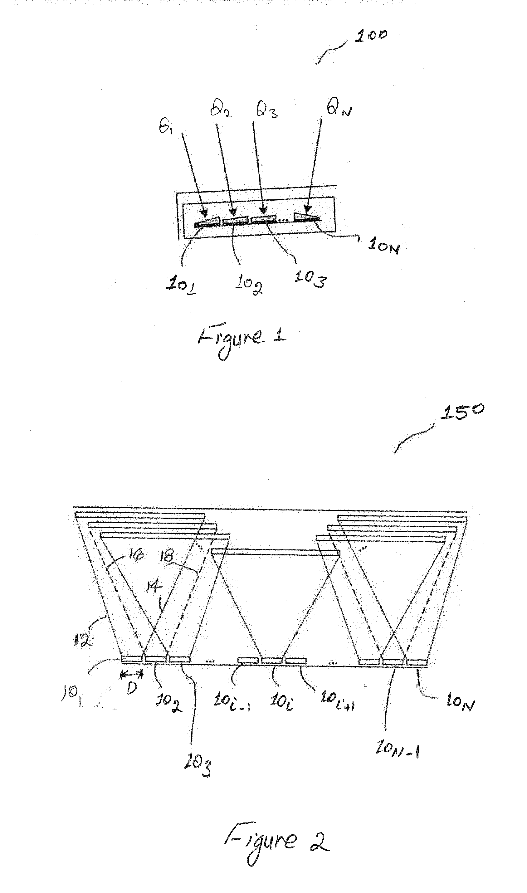
[0041] FIG. 1 is a simplified high-level side view of an incoherent/coherent lens-less imaging device 100, in accordance with one embodiment of the present invention. Imaging device 100 is shown as including N directionally sensitive optical receivers (alternatively referred to herein as pixels or detectors) 10.sub.1, 10.sub.2, 10.sub.3 . . . 10.sub.N that are shown as being respectively sensitive to light received from directions .theta..sub.1, .theta..sub.2 . . . .theta..sub.N. Imaging device 100 operates as described below.
[0042] In an incoherent/coherent imaging system, the phasor amplitudes received from different points on a target are uncorrelated since the illumination is spatially incoherent. Equation (1) below shows the relationship between the light intensity of an image of a target and the light intensity emanating from target along the x-direction for a one-dimensional array of pixels:
I.sub.IM(f.sub.x)=|H(f.sub.x)|.sup.2I.sub.TAR(f.sub.x)=H(f.sub.x)I.sub.T- AR(f.sub.x) (1)
[0043] In equation (1), I.sub.IM(f.sub.x) represents the image light intensity shown as being a function of the Fourier transform of the received light intensity along the x-direction, H(f.sub.x) is the optical transfer function providing a mapping between the target and its image, |H(f.sub.x)|.sup.2 represents that square of the absolute value of H(f.sub.x), and I.sub.TAR(f.sub.x) represents the target light intensity shown as being a function of the Fourier transform of the light intensity emanating from the target along the x-direction.
[0044] In a two-dimensional space, the optical transfer function may be represented by the following expression:
H ( f x , f y ) = FT { h 2 ( u , v ) } .intg. .intg. .infin. - .infin. h ( u , v ) 2 dudv ( 2 ) ##EQU00001##
[0045] In equation (2), h(u, v) represents the point-spread function associated with the imaging system, FT represents the Fourier transform operation, and (u, v) are variables representing positions along the x-y axis.
[0046] Using Parseval's identity, it is seen that:
H ( f x , f y ) = .intg. .intg. .infin. - .infin. H ( p + f x 2 , q + f y 2 ) H * ( p - f x 2 , q - f y 2 ) dpdq .intg. .intg. .infin. - .infin. H ( p , q ) 2 dpdq ( 3 ) ##EQU00002##
[0047] In equation (3), p and q are variables used in the integration. Accordingly, the optical transfer function H(f.sub.x,f.sub.y) is the normalized autocorrelation function of the amplitude transfer function (ATF). Geometrically, the optical transfer function is the overlap area of the ATF with a spatially shifted version of the ATF divided by the total area of the ATF.
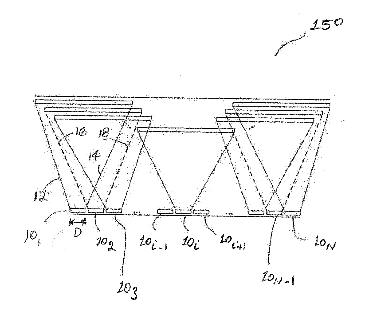
[0048] FIG. 2 is a simplified high-level side view of an incoherent lens-less imaging device 150, in accordance with one embodiment of the present invention, that includes N pixels 10.sub.1 . . . 10.sub.N. Also shown in FIG. 2 are the fields of views of pixels 10.sub.1 . . . 10.sub.N each defined by the pixel's optical transfer function H. Each such pixel 10.sub.i, where i is an index ranging from 1 to N, has a field of view and a transfer function, that overlaps with a transfer function of a multitude of neighboring pixels 10.sub.i-m . . . 10.sub.i-1, 10.sub.i+1, 10.sub.i+m as is also seen in the overlapping fields of views shown in FIG. 2, where m is an integer. For example, the field of view of pixel 10.sub.1 is shown as disposed between lines 12, 14, and the field of view of pixel 10.sub.2 is shown as disposed between lines 16, 18. For a pixel with a width of D, the effective angular receiving area has the following diffraction limit:
d .theta. = 1.22 .lamda. D ##EQU00003##
[0049] In accordance with one embodiments of the present invention, because each pixel 10 is sensitive to the light received from a different direction, each pixel captures the incident light differently. The intensity of the light arriving at the angle .theta. near the center of pixel 10.sub.i, namely I.sub.im.sub.i (.theta.), may be defined as shown below:
|.sub.im.sub.i(.theta.)=H.sub.i(.theta.)*I.sub.tar(.theta.)=.intg.H.sub.- i(.theta.)I.sub.tar(.theta.)d.theta. (4)
[0050] In equation (4), H.sub.i(.theta.) represents the optical transfer function of pixel 10.sub.i, I.sub.tar(.theta.) represents the intensity of the light received from the target, and * denotes the convolution operation.
[0051] Since the imaging device has N pixels, the intensity of the light received by the N pixels may be represented by vector {right arrow over (I)}.sub.im(.theta.) defined as shown below:
{right arrow over (I)}.sub.im(.theta.)={right arrow over (H)}.sub.i(.theta.)*{right arrow over (I)}.sub.tar (5)
[0052] In Equation (5), each entry in vector {right arrow over (I.sub.im)}(.theta.) represents the average light intensity received along the direction .theta., {right arrow over (H)}(.theta.) represents the vector of transfer functions, and {right arrow over (I)}.sub.tar(.theta.) represents the average light intensity emanating from the target along the direction .theta..
[0053] Each vector in equation (5) may be represented by a matrix. Assuming M represents the discretization of the values in equation (5), vector {right arrow over (I)}.sub.im may be represented by a 1.times.N matrix Y, vector {right arrow over (H)}(.theta.) may be represented by an N.times.M matrix H, and vector {right arrow over (I)}.sub.tar may be represented by an 1.times.M matrix I:
I = ( I 1 I M ) ##EQU00004## H = ( H 11 H 1 M H N 1 H NM ) ##EQU00004.2## Y = ( Y 1 Y N ) ##EQU00004.3##
[0054] Accordingly, equation (5) may be shown in a matrix form as:
Y=HI (6)
[0055] Referring to equation (6) because the matrix Y is obtained by the imaging device, in accordance with the present invention, and the transfer functions of the pixels represented by matrix H is also known, as described further below, the image of the target represented by matrix I can be computed.
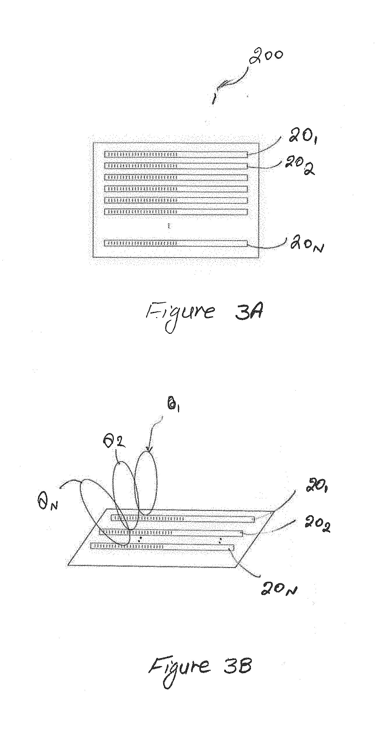
[0056] FIG. 3A is a simplified view of a one-dimensional lens-less imaging device 200, in accordance with one embodiment of the present invention. Imaging device 200 is shown as including N grating couplers 20.sub.1, 20.sub.2 . . . 20.sub.N each adapted to have a different response characteristic to the light received from a target whose image is being formed by the imaging device. As shown, for example, in FIG. 3B, grating coupler 20.sub.1 is shown as being responsive to light arriving at angle .theta..sub.1, grating coupler 20.sub.2 is shown as being responsive to light arriving at angle .theta..sub.2, and grating coupler 20.sub.N is shown as being responsive to light arriving at angle .theta..sub.N.
[0057] In one embodiment, by changing the spacing(s) between the openings of a grating coupler, the sensitivity and responsiveness of the grating coupler to the angle of the incident light may be varied. Such angular/directional sensitivity/responsiveness is also referred to herein as angular view.
[0058] Referring to FIGS. 3A and 3B, assume that the incident light has a wavelength of 1550 nm and that each grating coupler (receiving element or pixel) is 0.1 mm long. Because the diffraction limit is nearly d.theta.=1.1 degrees for each such receiving element, to have a field-of-view (FOV) of, e.g., 120 degrees, nearly 111 receiving elements are needed in such an embodiment to reconstruct an image of the target. Assuming that the receiving elements have a 1 um pitch, the receiving aperture for the imaging device shown in FIGS. 3A and 3B is nearly 1 mm by 1 mm.
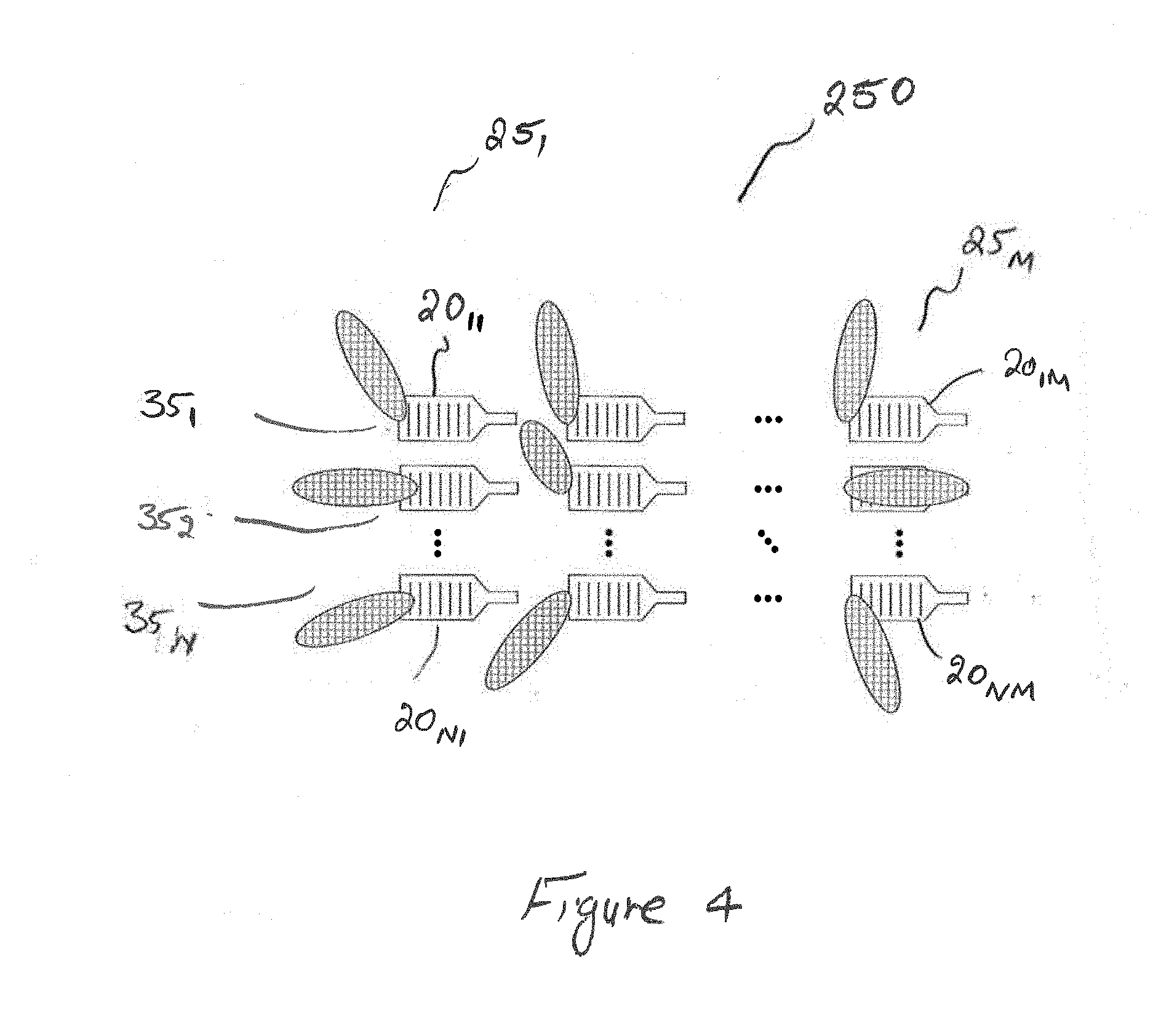
[0059] FIG. 4 is a simplified view of a two-dimensional lens-less imaging device 250, in accordance with one embodiment of the present invention. Imaging device 250 is shown as including N.times.M array of grating couplers. Row 35.sub.1 is shown as including grating couplers 20.sub.11, 20.sub.12 . . . 20.sub.1M. Likewise, row 35.sub.N is shown as including grating couplers 20.sub.N1, 20.sub.N2 . . . 20.sub.NM. Each grating coupler 20.sub.ij, where i is an index ranging from 1 to N and j is an index ranging from 1 to M, has a different angular view.
[0060] In accordance with another embodiment of the present invention, in addition to having different angular views, different pixels or different subsets of the pixels of a lens-less imaging device may have different responses to different wavelengths of the light. Such additional sensitivity to the light wavelength increases the information captured by the imaging device thus enabling it to form a higher resolution of the target image, reflected in the higher rank of the matrix represented by equation 6. In yet other embodiments, by forming pixels that have different responses to different wavelengths, an imaging device, in accordance with embodiments of the present invention, is adapted to form different images of the target for each different wavelength.
[0061] FIG. 5A is a simplified high-level side view of a lens-less imaging device 400, in accordance with one embodiment of the present invention. Imaging device 400 is shown as including N pixels 38.sub.i each of which is shown as including a transparent dielectric layer 35.sub.i overlaying a light detector 30.sub.i, where i is an index ranging from 1 to N. As seen from FIG. 5A, the slope of the dielectric layer formed over the light detectors is adapted to vary across the pixel array thereby causing the angular views of the pixels to be different from one another. For example, pixel 30.sub.8 is shown as having an angular view of .theta..sub.1, and pixel 38.sub.N is shown as having an angular view of .theta..sub.N. Although not shown in FIG. 5A, it is understood that the field of view of each pixel in the array overlaps with the fields of view of multitude of other pixels in the array.
[0062] FIG. 5B is a simplified high-level side view of a lens-less imaging device 410, in accordance with another embodiment of the present invention. Imaging device 410 is shown as including N pixels 48.sub.i each of which is shown as including a metallic wall 45.sub.i facing its associated detector 30.sub.i, where i is an index ranging from 1 to N. As seen from FIG. 5B, the angle between each detector and its associated wall facing the detector defines the angular view of the pixel. For example, the angle between detector 30.sub.1 and wall 45.sub.1 defines the angular view .theta..sub.1 of pixel 48.sub.1. Likewise, the angle between detector 30.sub.N and wall 45.sub.N defines the angular view .theta..sub.N of pixel 48.sub.N. Although not shown in FIG. 5B, it is understood that the field of view of each pixel in the array overlaps with the fields of view of multitude of other pixels in the array.
[0063] FIG. 5C is a simplified high-level side view of a lens-less imaging device 420, in accordance with another embodiment of the present invention. Imaging device 420 is shown as including N pixels 58.sub.i each of which is shown as including a detector 30.sub.1 and an associated micro electromechanical system (MEMS) component 55.sub.i, where i is an index ranging from 1 to N. As seen from FIG. 5C, the angle between each detector and its associated MEMS component defines the angular view of the pixel. For example, the angle between detector 30.sub.1 and its associated MEMS component 55.sub.1 defines the angular view .theta..sub.1 pixel 58.sub.i. Likewise, the angle between detector 30.sub.N and its associated MEMS component 55.sub.N defines the angular view .theta..sub.N of pixel 58.sub.N. By changing the angle of MEMS component 55.sub.i, the angular view .theta..sub.i of pixel 58.sub.i may be varied. It is understood that each MEMS component 55.sub.i diffracts the light it receives. Although not shown in FIG. 5C, it is understood that the field of view of each pixel in the array overlaps with the fields of view of multitude of other pixels in the array.
[0064] FIG. 5D is a simplified high-level side view of a lens-less imaging device 430, in accordance with another embodiment of the present invention. Imaging device 430 is shown as including N pixels 68.sub.i each of which is shown as including a detector 30.sub.i and an associated micro lens 65.sub.i, where i is an index ranging from 1 to N. As seen from FIG. 5D, the angle between each detector and its associated micro lens defines the angular view of the pixel. For example, the angle between detector 30.sub.1 and its associated micro lens 65.sub.1 defines the angular view .theta..sub.1 of pixel 68.sub.1. Likewise, the angle between detector 30.sub.N and its associated micro lens 55.sub.N defines the angular view .theta..sub.N of pixel 68N. By changing the angle of micro lens 55.sub.i, the angular view .theta..sub.1 of pixel 68.sub.i may be varied. It is understood that each micro lens 65.sub.i diffracts the light it receives. Although not shown in FIG. 5A, it is understood that the field of view of each pixel in the array overlaps with the fields of view of multitude of other pixels in the array. Although not shown, it is understood that the array of pixels shown in any one of the above FIGS. 5A-5D may be stacked so as to form a three-dimensional array to increase the amount of the light being captured and therefore enhance the image construction.
[0065] In some embodiments, the light captured by each pixel may have a Gaussian distribution. In some embodiments, the difference between the angular views of each pair of adjacent pixels may be the same. For example, in the embodiment, shown in FIG. 5A, the difference between .theta..sub.i and .theta..sub.i+1 may be selected to be the same for all i's. For each pixel, the intensity distribution pattern I.sub.c(.theta.) may be defined as:
I c ( .theta. ) = 1 .sigma. e - ( .theta. - .theta. c ) 2 2 .sigma. ( 7 ) ##EQU00005##
where .sigma. represents the beam width and (.theta.-.theta.c) represents the degree of deviation from the angular view of that pixel. For example, referring to FIG. 5A, pixel 38.sub.i is adapted to capture the highest amount of light from the light arriving at .theta..sub.i.
[0066] In yet other embodiments, the difference between the angular views of different pair of adjacent pixels may be randomly selected and may thus be different. Therefore, in such embodiment, the difference (.theta..sub.i-.theta..sub.i+1) may be different for different i's.
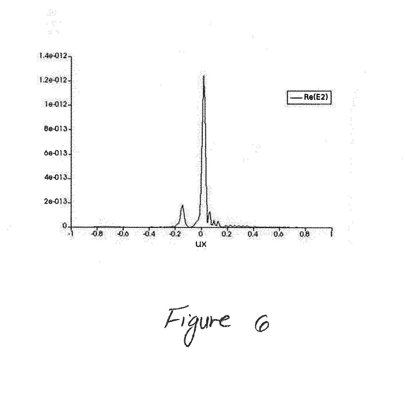
[0067] In some embodiments of the present invention, the light captured by the pixels does not have a Gaussian distribution pattern. FIG. 6 shows the intensity distribution pattern of the light captured by a grating coupler, such as the grating couplers 20.sub.i shown in FIGS. 3A and 3B. As is seen from FIG. 6, the intensity distribution pattern of the light captured by a grating coupler is not Gaussian.
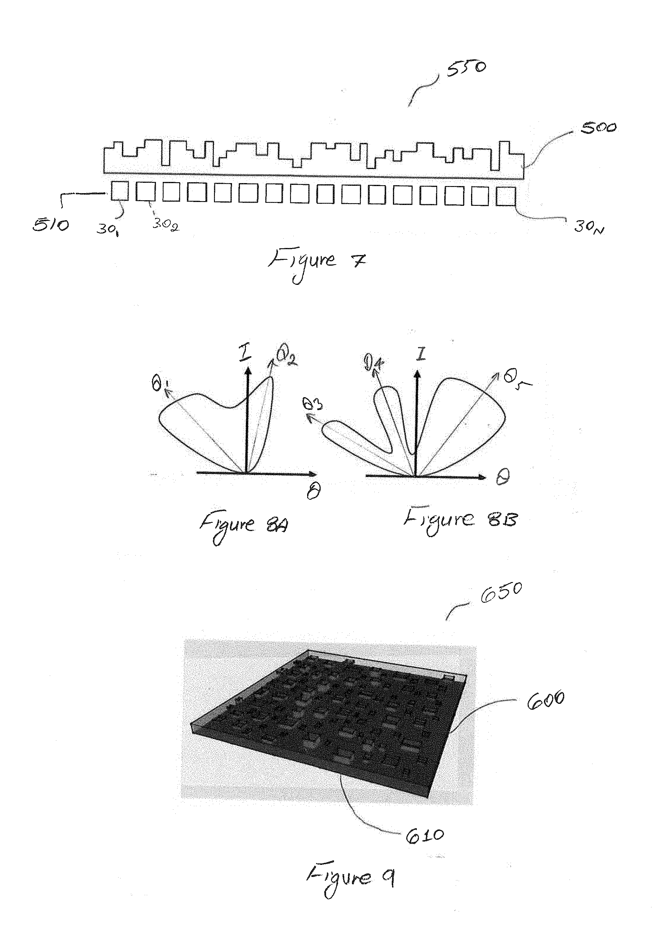
[0068] In accordance with one embodiment of the present invention, a lens-free imaging device includes a mapping layer formed over an array of detectors. FIG. 7 is a simplified cross-sectional view of a lens-free imaging device 550 shown as including a one-dimensional array 510 of detectors 30.sub.i and a mapping layer 500 overlaying detectors 30.sub.i. Mapping layer 500 is adapted to have a different geometrical shape for different light detectors positioned therebelow. The differing geometrical shapes thus ensure that different detectors have different angular views or response characteristics. FIGS. 8A and 8B are exemplary response patterns of two of the detectors of array 510 caused by differing geometrical shape of the mapping layer 500 overlaying the two detectors. Due to the presence of the overlaying mapping layer, the detector of FIG. 8A shows a maximum sensitivity to the light received from directions .theta..sub.1 and .theta..sub.2, and the detector of FIG. 8B shows a maximum sensitivity to the light received from directions .theta..sub.3, .theta..sub.4 and .theta..sub.5. By using the transfer function H of the mapping layer 500 associated with each detector together with the light received for each detector, as described above, the image of the target is formed.
[0069] FIG. 9 is a simplified perspective view of a lens-free imaging device 650 shown as including a two-dimensional array 610 of detectors and a mapping layer 600 overlaying the detectors. Mapping layer 600 is adapted to have a different geometrical shape for different light detectors positioned therebelow. The differing geometrical shapes ensure that the different underlaying detectors have different angular response patterns.
[0070] FIG. 10 is a computer simulation of the intensity distribution pattern of a one-dimensional receiver array of ten pixels each having a different Gaussian distribution pattern, in accordance with one embodiment of the present invention. As is seen from FIG. 10, each pixel has a different peak and angular view. As is also seen from FIG. 10, many of the distribution patterns overlap, in accordance with embodiment of the present invention.
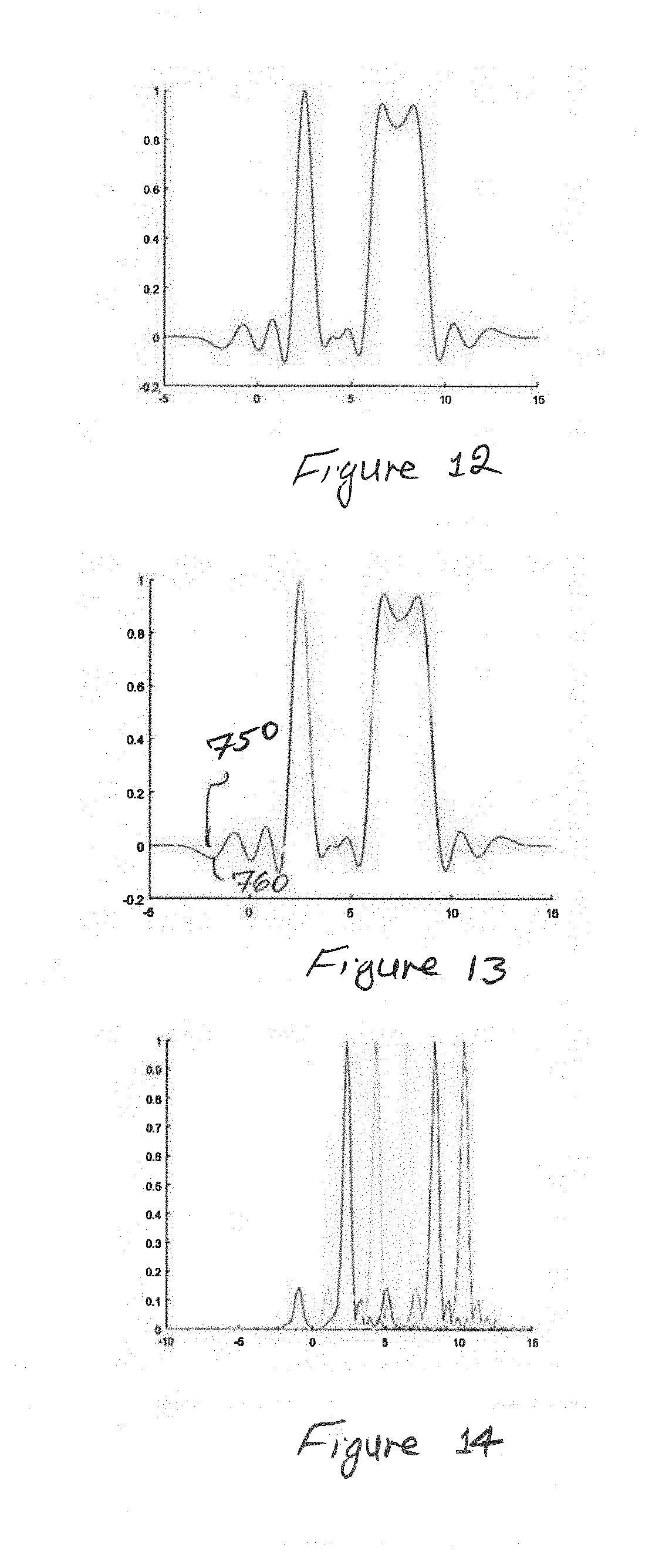
[0071] FIG. 11 shows the intensity distribution pattern of a target being imaged, in accordance with embodiments of the present invention. FIG. 12 shows a computer simulation of the image of the target of FIG. 11 constructed using a lens-less imaging device having a one-dimensional array of 20 pixels, in accordance with one embodiment of the present invention. By knowing the optical transfer function of each pixel as well as the response received from each such pixel, the image in FIG. 12 is formed, as described further above. Plot 750 of FIG. 13 shows a computer simulation of the image of the target of FIG. 11 constructed using a lens-less imaging device having a one-dimensional array of 100 pixels, in accordance with one embodiment of the present invention. Plot 760 of FIG. 13 shows the same image as that shown in FIG. 12. FIG. 14 shows the intensity distribution pattern of the grating couplers shown in FIG. 3A, in accordance with one embodiment of the present invention.
[0072] FIG. 15 is a color image of a target (CiT) being reconstructed using a lens-less imaging device, in accordance with one embodiment of the present invention. FIG. 16 is the response of a 10.times.10 array of receiving elements (pixels)--each adapted to have a different Gaussian distribution pattern as described above--to the target shown in FIG. 15. FIG. 17 shows the image of the target shown in FIG. 15 formed using the response shown in FIG. 16.
[0073] FIG. 18 is the response of a 100.times.100 array of pixels--each adapted to have a different Gaussian distribution pattern as described above--to the target shown in FIG. 15. FIG. 19 shows the image of the target shown in FIG. 15 formed using the response shown in FIG. 18.
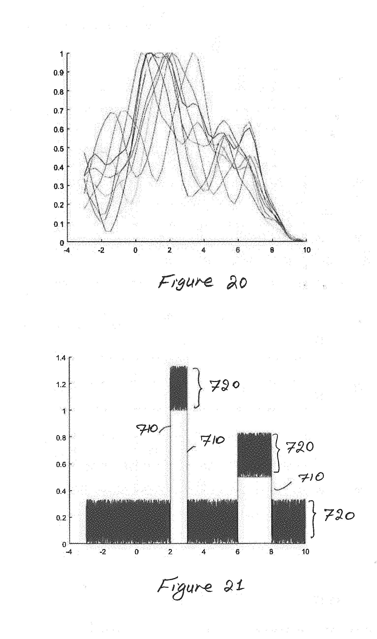
[0074] FIG. 20 shows a computer simulation of the intensity distribution pattern of a one-dimensional receiver array having a multitude of pixels, in accordance with one embodiment of the present invention. As is seen from FIG. 20, each pixel has a non-Gaussian distribution patterns with a different peak and angular view. As is also seen from FIG. 20, many of the distribution patterns overlap, in accordance with embodiment of the present invention.
[0075] FIG. 21 shows the intensity distribution pattern of a target 710 being imaged, in accordance with embodiments of the present invention. Also shown in FIG. 21 is noise 720 injected into the image. Plot 810 of FIG. 22 shows the image of target 710 of FIG. 20 without the injected noise 720. The image represented by plot 810 is formed using the one-dimensional receiver array with receiving elements having a non-Gaussian distribution pattern, as shown in FIG. 20. Plot 820 of FIG. 22 shows the image of target 710 of FIG. 20 with the injected noise 720. The image represented by plot 820 is formed using the one-dimensional receiver array with receiving elements having a non-Gaussian distribution pattern, as shown in FIG. 20. Also shown in FIG. 22 is image 710 of FIG. 21.
[0076] The above embodiments of the present invention are illustrative and not limitative. The embodiments of the present invention are not limited by the number of receiving elements or pixels in the array or the number of array dimensions. The above embodiments of the present invention are not limited by the wavelength or frequency of the light. Other modifications and variations will be apparent to those skilled in the art and are intended to fall within the scope of the appended claims.
* * * * *
D00000
D00001
D00002
D00003
D00004
D00005
D00006
D00007
D00008
D00009
D00010
D00011
D00012
D00013


XML
uspto.report is an independent third-party trademark research tool that is not affiliated, endorsed, or sponsored by the United States Patent and Trademark Office (USPTO) or any other governmental organization. The information provided by uspto.report is based on publicly available data at the time of writing and is intended for informational purposes only.
While we strive to provide accurate and up-to-date information, we do not guarantee the accuracy, completeness, reliability, or suitability of the information displayed on this site. The use of this site is at your own risk. Any reliance you place on such information is therefore strictly at your own risk.
All official trademark data, including owner information, should be verified by visiting the official USPTO website at www.uspto.gov. This site is not intended to replace professional legal advice and should not be used as a substitute for consulting with a legal professional who is knowledgeable about trademark law.