Techniques for Providing a Haptic Output and Sensing a Haptic Input Using a Piezoelectric Body
Zhang; Zhipeng ; et al.
U.S. patent application number 15/653468 was filed with the patent office on 2019-01-24 for techniques for providing a haptic output and sensing a haptic input using a piezoelectric body. The applicant listed for this patent is Apple Inc.. Invention is credited to Richard H. Koch, Teera Songatikamas, Zhipeng Zhang.
| Application Number | 20190027674 15/653468 |
| Document ID | / |
| Family ID | 65023211 |
| Filed Date | 2019-01-24 |


View All Diagrams
| United States Patent Application | 20190027674 |
| Kind Code | A1 |
| Zhang; Zhipeng ; et al. | January 24, 2019 |
Techniques for Providing a Haptic Output and Sensing a Haptic Input Using a Piezoelectric Body
Abstract
Haptic interfaces are described. One haptic interface includes a piezoelectric body and first and second electrodes coupled to the piezoelectric body. The haptic interface also includes a control circuit. The control circuit includes a haptic actuator, a haptic sensor circuit, and an overcurrent protection circuit. The haptic actuator circuit is coupled to the first electrode and configured to charge the piezoelectric body. The charging causes the piezoelectric body to provide a haptic output. The haptic sensor circuit is coupled to the second electrode and configured to sense an electrical change at the second electrode. The electrical change is related to a haptic input received by the piezoelectric body. The overcurrent protection circuit is coupled to the second electrode and configured to limit a current flow into the haptic sensor circuit while the haptic actuator circuit is charging the piezoelectric body.
| Inventors: | Zhang; Zhipeng; (Santa Clara, CA) ; Koch; Richard H.; (Cupertino, CA) ; Songatikamas; Teera; (San Jose, CA) | ||||||||||
| Applicant: |
|
||||||||||
|---|---|---|---|---|---|---|---|---|---|---|---|
| Family ID: | 65023211 | ||||||||||
| Appl. No.: | 15/653468 | ||||||||||
| Filed: | July 18, 2017 |
| Current U.S. Class: | 1/1 |
| Current CPC Class: | H01L 41/0825 20130101; G06F 1/1643 20130101; G06F 3/0412 20130101; G06F 3/0416 20130101; H01L 41/0472 20130101; H01L 41/083 20130101; H01L 41/042 20130101; G06F 3/041 20130101; G06F 2203/04103 20130101; H01L 41/09 20130101; G06F 3/016 20130101; G06F 3/04886 20130101 |
| International Class: | H01L 41/047 20060101 H01L041/047; H01L 41/083 20060101 H01L041/083; H01L 41/09 20060101 H01L041/09; G06F 3/041 20060101 G06F003/041; G06F 3/0488 20060101 G06F003/0488 |
Claims
1. A haptic interface, comprising: a piezoelectric body; a first electrode coupled to the piezoelectric body; a second electrode coupled to the piezoelectric body; and a control circuit, comprising: a haptic actuator circuit coupled to the first electrode and configured to charge the piezoelectric body, the charging causing the piezoelectric body to provide a haptic output; a haptic sensor circuit coupled to the second electrode and configured to sense an electrical change at the second electrode, the electrical change related to a haptic input received by the piezoelectric body; and an overcurrent protection circuit coupled to the second electrode and configured to limit a current flow into the haptic sensor circuit while the haptic actuator circuit is charging the piezoelectric body.
2. The haptic interface of claim 1, wherein the overcurrent protection circuit comprises: a transistor coupled between the second electrode and a discharge node, the transistor having a control input configured to receive a signal that causes the transistor to open or close a current path between the second electrode and the discharge node.
3. The haptic interface of claim 1, wherein the overcurrent protection circuit comprises: a clamper circuit coupled between the second electrode and a discharge node.
4. The haptic interface of claim 3, wherein the clamper circuit comprises a forward-biased diode coupled in parallel with a reverse-biased diode.
5. The haptic interface of claim 1, wherein the haptic sensor circuit comprises a sense amp, the sense amp comprising a negative input coupled to the second electrode and a positive input coupled to a discharge node.
6. The haptic interface of claim 5, wherein the overcurrent protection circuit is coupled between the negative input and the positive input of the sense amp, and the positive input of the sense amp is coupled to the discharge node.
7. The haptic interface of claim 5, wherein the overcurrent protection circuit comprises: a transistor coupled between the negative input and the positive input of the sense amp, the transistor having a control input configured to receive a control signal that causes the transistor to open or close a current path between the negative input and the positive input of the sense amp, wherein the positive input of the sense amp is further coupled to the discharge node.
8. The haptic interface of claim 7, wherein the haptic actuator circuit comprises: a second transistor coupled between the first electrode and a power source, the second transistor having a second control input configured to receive a second control signal that causes the second transistor to open or close a second current path between the first electrode and the power source; and a third transistor coupled between the first electrode and the discharge node, the transistor having a third control input configured to receive a third control signal that causes the third transistor to open or close a third current path between the first electrode and the discharge node.
9. The haptic interface of claim 5, wherein the overcurrent protection circuit comprises: a charge integration capacitor coupled between the negative input of the sense amp and an output of the sense amp.
10. The haptic interface of claim 9, further comprising: an integrated charge discharge circuit coupled to the charge integration capacitor, the integrated charge discharge circuit having a control input configured to receive a control signal that causes the integrated charge discharge circuit to discharge a charge integrated by the charge integration capacitor.
11. The haptic interface of claim 5, further comprising: a digital sampling circuit coupled to an output of the sense amp.
12. A haptic interface, comprising: a piezoelectric body; a first electrode coupled to the piezoelectric body; a second electrode coupled to the piezoelectric body; and a control circuit, comprising: a haptic actuator circuit coupled to the first electrode and configured to maintain a charge on the piezoelectric body, the charge causing the piezoelectric body to provide a haptic output; and a haptic sensor circuit coupled to the second electrode and configured to sense an electrical change at the second electrode while the piezoelectric body is charged, the electrical change related to a haptic input received by the piezoelectric body.
13. A method of operating a haptic interface, comprising: charging a piezoelectric body of the haptic interface to deliver a haptic output; limiting a current flow into a haptic sensor circuit while charging the piezoelectric body; and monitoring for a haptic input to the piezoelectric body using the haptic sensor circuit while the piezoelectric body is charged.
14. The method of claim 13, further comprising: monitoring for the haptic input while charging the piezoelectric body.
15. The method of claim 13, wherein limiting the current flow into the haptic sensor circuit comprises: diverting at least a portion of the current flow from into the haptic sensor circuit to a discharge node.
16. The method of claim 15, wherein diverting at least the portion of the current flow from into the haptic sensor circuit to the discharge node comprises: applying a control signal to a transistor.
17. The method of claim 16, wherein the transistor is coupled between a first input and a second input of the haptic sensor circuit.
18. The method of claim 17, wherein the first input is coupled to an electrode attached to the piezoelectric body, and the second input is coupled to the discharge node.
19. The method of claim 15, wherein diverting at least the portion of the current flow from into the haptic sensor circuit to the discharge node comprises: automatically diverting at least the portion of the current flow based on a parameter of a diode.
20. The method of claim 13, wherein limiting the current flow into the haptic sensor circuit comprises: integrating a charge using a charge integrator coupled between an input of the haptic sensor circuit and an output of the haptic sensor circuit; and clearing the integrated charge before monitoring for the haptic input.
Description
FIELD
[0001] The present disclosure generally relates to haptic interfaces, and to techniques for providing a haptic output and sensing a haptic input using a piezoelectric body. The haptic output may be provided by actuating the piezoelectric body.
BACKGROUND
[0002] Electronic devices are commonplace in today's society. Some electronic devices incorporate a haptic interface (e.g., a haptic input or output system). An electronic device with a haptic interface may activate the haptic interface to solicit a user's attention, enhance the user's interaction experience with the electronic device, displace the electronic device or a component of the electronic device, or provide any other suitable notification or user experience. An electronic device with a haptic interface may also, or alternatively, receive a force input from a user via the haptic interface, and in response to the force input, wake up a portion of the electronic device, manipulate a graphical element on a display of the electronic device, or perform another operation in response to the force input.
[0003] Piezoelectric materials can convert between mechanical energy and electrical energy. A piezoelectric material (or piezoelectric body) may be used to convert mechanical energy into electrical energy using what has been referred to as the direct piezoelectric effect. Conversion of mechanical energy into electrical energy can be used to sense a mechanical force or pressure on, or displacement of, a piezoelectric body. A piezoelectric body may also, or alternatively, convert electrical energy into mechanical energy using what has been referred to as the inverse piezoelectric effect. Conversion of electrical energy into mechanical energy can be used to actuate a piezoelectric body and, in some cases, move or displace the piezoelectric body.
[0004] One application for piezoelectric bodies is in haptic interfaces of electronic devices. The direct piezoelectric effect can be used to sense a haptic input to the haptic interface (e.g., a user's force or pressure on, or displacement of, a piezoelectric body included in a haptic interface). The inverse piezoelectric effect can be used to provide a haptic output via the haptic interface (e.g., a piezoelectric body may be electrically charged to cause the piezoelectric body to produce a force, pressure, or displacement that can be perceived by a user of the haptic interface).
SUMMARY
[0005] The present disclosure is directed to haptic interfaces, and to techniques for providing a haptic output and sensing a haptic input using a piezoelectric body. In particular, the present disclosure describes a control circuit for a piezoelectric body of a haptic interface. The control circuit may be used to both actuate the piezoelectric body, to provide a haptic output, and to sense an electrical change corresponding to a haptic input received by the piezoelectric body. In some embodiments, a piezoelectric body may be simultaneously actuated and sensed. In some embodiments, the control circuit may include an overcurrent protection circuit that limits current flow into a sensing portion of the control circuit while an actuation portion of the control circuit is charging the piezoelectric body. The overcurrent protection circuit may be needed because a haptic actuation signal provided by the actuation portion of the control circuit may be sensed by the sensing portion of the control circuit, and may be one or more orders of magnitude greater than a haptic input signal intended to be sensed by the sensing portion of the control circuit. The haptic actuation signal could therefore damage the sensing portion of the control circuit in the absence of an overcurrent protection circuit.
[0006] In a first aspect of the present disclosure, a haptic interface is described. The haptic interface may include a piezoelectric body and first and second electrodes coupled to the piezoelectric body. The haptic interface may also include a control circuit. The control circuit may include a haptic actuator circuit, a haptic sensor circuit, and an overcurrent protection circuit. The haptic actuator circuit may be coupled to the first electrode and configured to charge the piezoelectric body. The charging may cause the piezoelectric body to provide a haptic output. The haptic sensor circuit may be coupled to the second electrode and configured to sense an electrical change at the second electrode. The electrical change may be related to a haptic input received by the piezoelectric body. The overcurrent protection circuit may be coupled to the second electrode and configured to limit a current flow into the haptic sensor circuit while the haptic actuator circuit is charging the piezoelectric body.
[0007] In another aspect of the present disclosure, another haptic interface is described. The haptic interface may include a piezoelectric body and first and second electrodes coupled to the piezoelectric body. The haptic interface may also include a control circuit. The control circuit may include a haptic actuator circuit, a haptic sensor circuit, and an overcurrent protection circuit. The haptic actuator circuit may be coupled to the first electrode and configured to maintain a charge on the piezoelectric body. The charge may cause the piezoelectric body to provide a haptic output. The haptic sensor circuit may be coupled to the second electrode and configured to sense an electrical change at the second electrode while the piezoelectric body is charged. The electrical change may be related to a haptic input received by the piezoelectric body.
[0008] In yet another aspect of the present disclosure, a method of operating a haptic interface is described. The method may include charging a piezoelectric body of the haptic interface to deliver a haptic output, limiting a current flow into a haptic sensor circuit while charging the piezoelectric body, and monitoring for a haptic input to the piezoelectric body using the haptic sensor circuit while the piezoelectric body is charged.
[0009] In addition to the exemplary aspects and embodiments described above, further aspects and embodiments will become apparent by reference to the drawings and by study of the following description.
BRIEF DESCRIPTION OF THE DRAWINGS
[0010] The present disclosure will be readily understood by the following detailed description in conjunction with the accompanying drawings, wherein like reference numerals designate like structural elements, and in which:
[0011] FIG. 1 shows a front view of an electronic device incorporating a sample haptic interface;
[0012] FIGS. 2A and 2B show a first anchoring configuration that may be used for a piezoelectric body of a haptic interface;
[0013] FIGS. 3A and 3B show a second anchoring configuration that may be used for a piezoelectric body of a haptic interface;
[0014] FIGS. 4A and 4B show a third anchoring configuration that may be used for a piezoelectric body of a haptic interface;
[0015] FIGS. 5A, 5B, and 5C show sample constructions of a piezoelectric body that may be used in a haptic interface;
[0016] FIG. 6 shows a cross-section of a piezoelectric body attached to first and second electrodes;
[0017] FIG. 7 shows a block diagram of a haptic interface capable of providing a haptic output and sensing a haptic input;
[0018] FIG. 8 shows a sample first circuit schematic for a haptic interface;
[0019] FIG. 9 shows a graph of voltage at the second electrode, over time, for various charging scenarios of the piezoelectric body shown in FIG. 8;
[0020] FIG. 10 shows a sample second circuit schematic for a haptic interface;
[0021] FIG. 11 shows a sample third circuit schematic for a haptic interface;
[0022] FIG. 12 shows a sample fourth circuit schematic for a haptic interface;
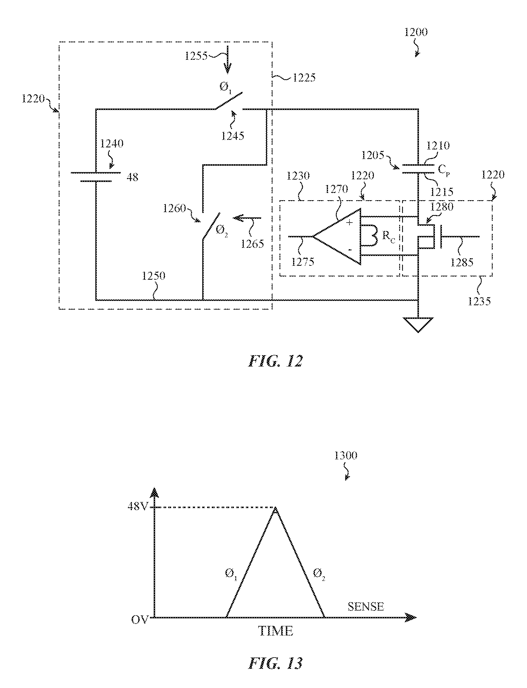
[0023] FIG. 13 shows a graph of voltage at the second electrode, over time, for various charging scenarios of the piezoelectric body shown in FIG. 12;
[0024] FIGS. 14 and 15 show electronic devices that may incorporate haptic interfaces;
[0025] FIGS. 16 and 17 show methods of operating a haptic interface; and
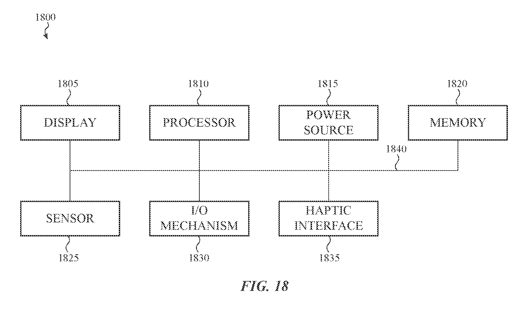
[0026] FIG. 18 shows a sample electrical block diagram of an electronic device.
DETAILED DESCRIPTION
[0027] Reference will now be made in detail to representative embodiments illustrated in the accompanying drawings. It should be understood that the following description is not intended to limit the description to a preferred embodiment. To the contrary, it is intended to cover alternatives, modifications, and equivalents to the described embodiments, as can be included within the spirit and scope of the described embodiments as defined by the appended claims.
[0028] The embodiments described herein are directed to a haptic interface that receives and provides localized haptic inputs and output for an electronic device. The haptic interface may include a set of piezoelectric bodies (e.g., synthetic ceramic bodies (e.g., lead zirconate titanate (PZT) bodies), lead-free piezoceramic bodies (e.g., sodium potassium niobate bodies), natural crystal bodies (e.g., quartz bodies, synthetic crystal bodies, and so on), and may provide or be coupled to a surface such as, for example, a cover glass or display of the electronic device. When a piezoelectric body of the haptic interface is compressed, deflected, deformed, or otherwise moved by a haptic input (e.g., by a user or structure, such as a user intending to press a key of a keyboard or a button), the compression, deflection, deformation, or other movement may be measured, and a signal corresponding to the compression, deflection, deformation, or other movement may be received by a processor of the electronic device. In some cases, the processor may wake up a portion of the electronic device, manipulate a graphical element on a display of the electronic device, clear a notification, stop a timer, or perform another operation in response to the signal. The processor may also activate the haptic interface (e.g., by generating an electric field that causes one or more piezoelectric bodies to compress, deflect, deform, rapidly change shape (e.g., vibrate), or otherwise physically change) to solicit a user's attention, enhance the user's interaction experience with the electronic device, displace the electronic device or a component of the electronic device, or provide any other suitable notification or user experience.
[0029] In some examples, a compression, deflection, deformation, or other movement of a piezoelectric body may cause a change in voltage between electrodes attached to the piezoelectric body. Conversely, a processor may apply an electric current or voltage to the electrodes to cause the piezoelectric body to compress, deflect, deform, vibrate, or otherwise move.
[0030] In some implementations, the size, change, state, or rate of change in a piezoelectric body may be related to the amount of compression, deflection, deformation, or movement of the haptic interface and, as a result, the magnitude or strength of haptic input or output. Thus, the greater the change in compression, deflection, deformation, or other movement of a piezoelectric body, the greater the haptic input (e.g., force input) or haptic output (e.g., force output).
[0031] A panel-sized vibration actuator (e.g., for display panel haptic applications) can be constructed with multiple piezoelectric bodies assembled on a flex circuit or sandwiched between flex circuits. In such an architecture, two electrodes may be positioned on opposite faces of each piezoelectric body. For example, a top electrode can be formed on a top face of a piezoelectric body and a bottom electrode can be formed on a bottom face of the piezoelectric body. In some cases, the bottom electrode can wrap around a sidewall of the piezoelectric body. In such a configuration, the top electrode and the bottom electrode may both occupy a portion of the top face of the piezoelectric body.
[0032] A set of piezoelectric bodies, each with corresponding electrodes, may be sandwiched between first and second substrates, such as first and second flex circuits, or a flex circuit and a stiffener. Each piezoelectric body may be electrically connected to the first or second substrate. For example, a first electrical connection can be made between a top electrode of a piezoelectric body and an electrical conductor on or within a top flex circuit, and a second electrical connection can be made between a bottom electrode of the piezoelectric body and an electrical conductor on or within a bottom flex circuit.
[0033] The first and second electrical connections can be established using any number of suitable techniques including, but not limited to, soldering, welding, bonding with a conductive adhesive, bonding with a conductive tape, placing conductive surfaces in contact, and so on.
[0034] In some use cases, it may be useful to sense a haptic input while providing a haptic output. In some cases, a haptic input and haptic output may be sensed/provided by different piezoelectric bodies and respective control circuits, because haptic actuation signals may be orders of magnitude greater than haptic input signals (e.g., milliamps versus nano-Coulombs), making piezoelectric actuation and sensing circuits incompatible. In other cases, and as described in the present disclosure, piezoelectric actuation and sensing circuits may be used in conjunction with a single piezoelectric body (or single set of piezoelectric bodies) by using an overcurrent protection circuit to protect the sensing circuit during time periods when the charging of a piezoelectric body may damage the sensing circuit. When piezoelectric actuation and sensing circuits are combined, haptic input to a piezoelectric body may be sensed while the piezoelectric body is charged (and also while the piezoelectric is not charged).
[0035] Techniques are described for providing a haptic output and sensing a haptic input using a piezoelectric body. In some embodiments, the techniques limit a current flow into a haptic sensor circuit while charging a piezoelectric body to deliver a haptic output, and enable monitoring for a haptic input to the piezoelectric body while the piezoelectric body is charged. This and other embodiments are discussed in more detail below, with reference to FIGS. 1-18. However, those skilled in the art will readily appreciate that the detailed description given herein with respect to these figures is for explanation only and should not be construed as limiting.
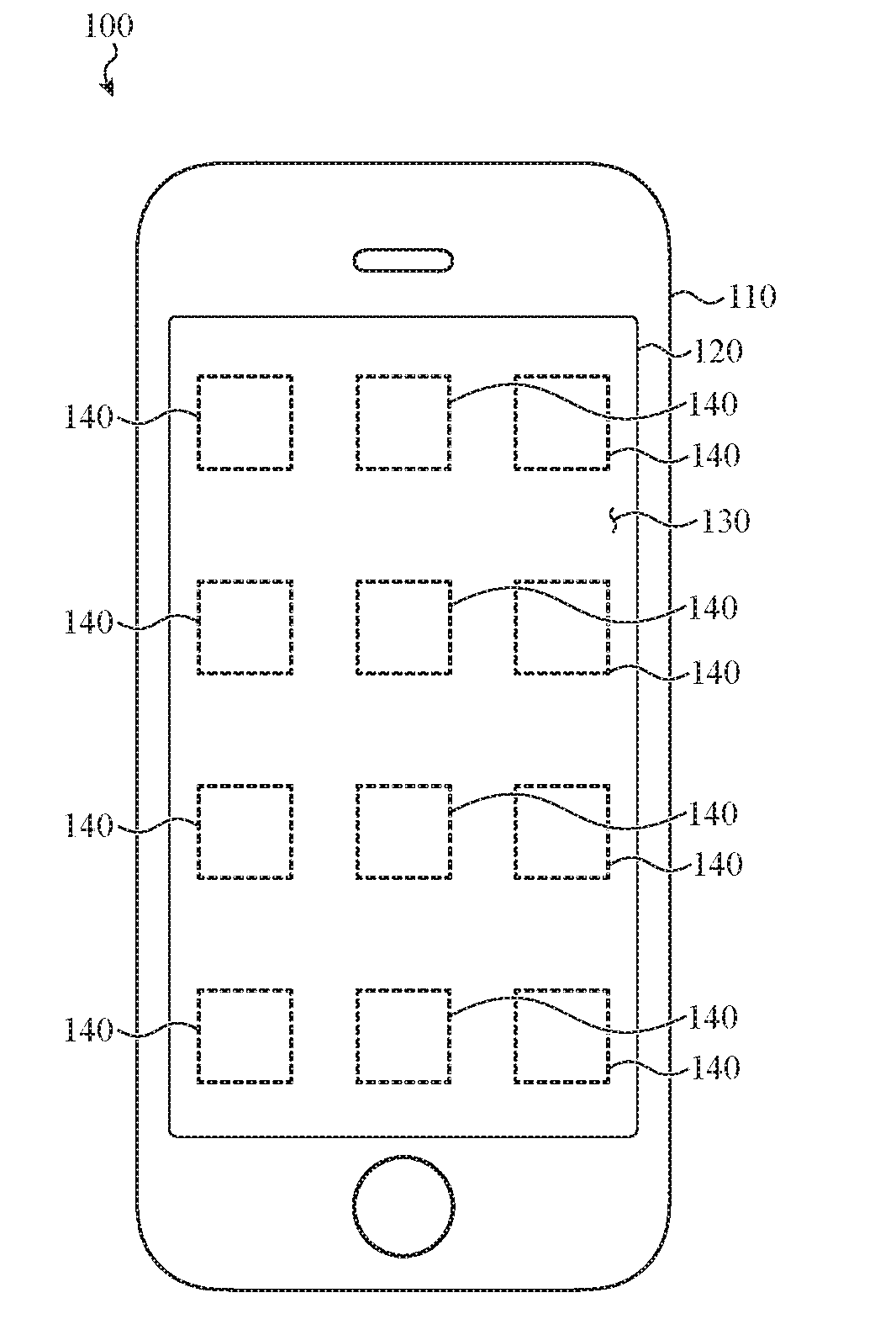
[0036] FIG. 1 shows a front view of an electronic device 100 incorporating a sample haptic interface, such as one of the haptic interfaces described herein. The electronic device 100 is illustrated as a smartphone, although this is not required and other electronic devices can incorporate the haptic interfaces described herein. These include, but are not limited to, wearable devices, tablet computers, cellular devices, peripheral input devices, game controllers, vehicle control circuits, laptop computers, industrial control circuits, consumer appliances, industrial machinery, and so on.
[0037] In the illustrated embodiment, the electronic device 100 includes a housing 110 to retain, support, and/or enclose various components of the electronic device 100, such as a display 120. The housing 110 may be a unitary housing, a housing that includes a front piece secured to a back piece, or a housing that includes any number or arrangement of pieces. The display 120 can include a stack of multiple layers including, for example, and in no particular order: a light-emitting display layer (e.g., an organic light emitting diode (OLED) layer), a cover layer, a touch input layer, a haptic interface layer, a biometric layer, and so on. Other embodiments can implement the display 120 in a different manner, such as with liquid crystal display (LCD) technology, electronic ink technology, quantum dot technology, organic electro luminescence (OEL) technology, or other light-emitting display technologies. The light-emitting display layer may be viewable through one or more of the other layers. Other embodiments can also include different numbers of layers. In some embodiments, a protective outer layer of the display 120 may define an input surface 130.
[0038] Regardless of the implementation-specific display technology or technologies selected for a particular embodiment, the various layers of the display 120 may be adhered together with an optically transparent adhesive and/or may be supported by a common frame such that the layers abut one another.
[0039] The common frame can be made from any suitable material such as, but not limited to: metal, plastic, ceramic, acrylic, and so on. The common frame may be a multi-purpose component serving an additional function such as, but not limited to: providing an environmental and/or hermetic seal to one or more components of the display 120 or the electronic device 100; providing structural support to the housing 110; providing pressure relief to one or more components of the display 120 or the electronic device 100; providing and defining gaps between one or more layers of the display 120 for thermal venting and/or to permit flexing of the layers in response to a force (input or output) applied to the input surface 130; and so on.
[0040] In some embodiments, the layers of the display 120 may be attached or deposited onto separate substrates that may be laminated or bonded to each other. The display 120 may also include or be positioned adjacent to other layers suitable for improving the structural or optical performance of the display 120, including, but not limited to, a cover glass sheet, polarizer sheets, color masks, and the like. Additionally, the display 120 may include a touch sensor (not shown) for determining the location of one or more touches on the input surface 130 of the electronic device 100. In some embodiments, the touch sensor may be a capacitive touch sensor configured to detect the location and/or area of one or more touches of a user's finger and/or a passive or active stylus on the input surface 130. The electronic device 100 may also include a haptic structure (e.g., a piezoelectric body) for both 1) providing a haptic output to a user of the electronic device 100 and 2) receiving a haptic input from the user.
[0041] The electronic device 100 can also include a processor, memory, power supply and/or battery, network connections, sensors, input/output mechanisms (e.g., devices or ports), acoustic elements, haptic elements, digital and/or analog circuits for performing and/or coordinating tasks of the electronic device 100, and so on. For simplicity of illustration, the electronic device 100 is depicted in FIG. 1 without many of these elements, each of which may be included, partially and/or entirely, within the housing 110 and may be operationally or functionally associated with, or coupled to, the display 120.
[0042] One or more haptic structures (e.g., piezoelectric bodies 140) of a haptic interface can be disposed below the input surface 130. The haptic structures may be arranged in an array or other pattern and positioned behind or within the display 120, although haptic structures may also or alternatively be positioned behind or within non-display portions of the electronic device 100, such as in sidewalls, rear walls, non-display portions of a front of the electronic device 100, on a back side of the electronic device 100, and so on. As a result of this arrangement, each haptic structure can provide localized haptic output, or receive local haptic input, to/from a user touching the display 120. The haptic structures may be of any suitable size or shape.
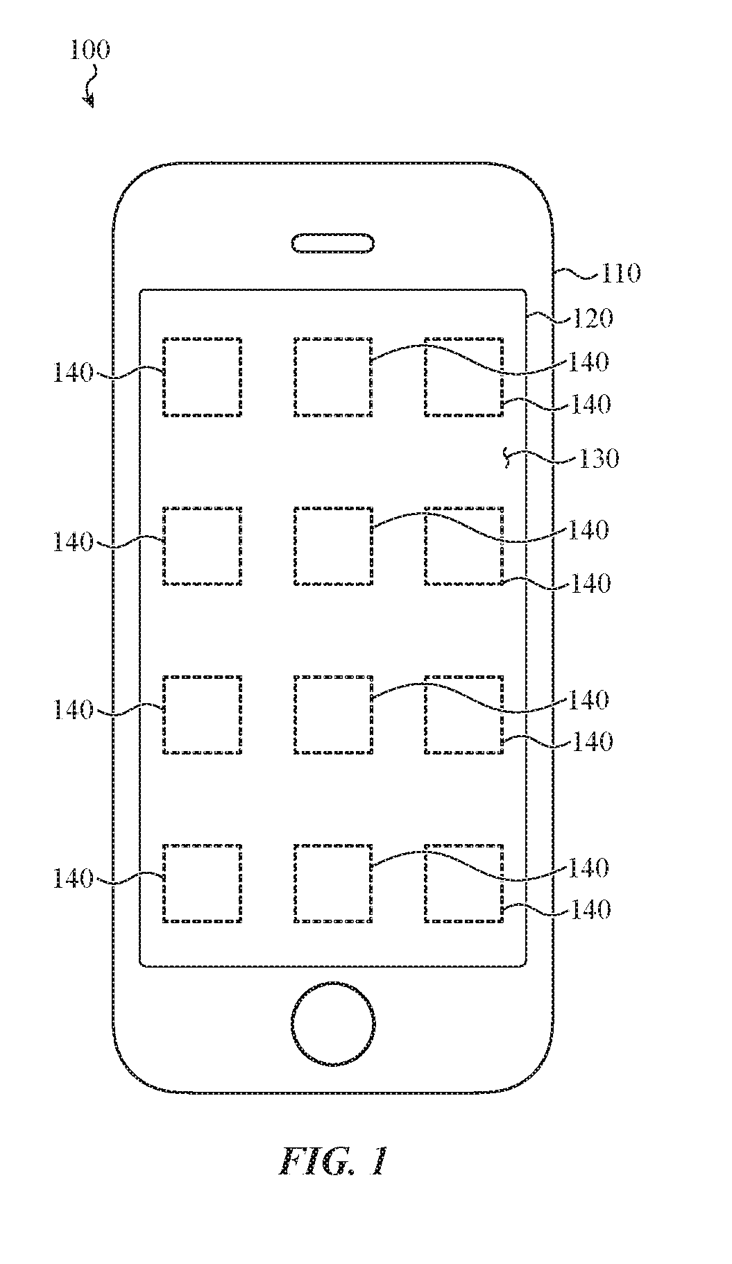
[0043] FIGS. 2A, 2B, 3A, 3B, 4A, and 4B show various anchoring configurations for piezoelectric bodies that may be used in conjunction with a haptic interface such as the haptic interface described with reference to FIG. 1. The anchoring configurations shown are examples only, and are not intended to limit the types of anchoring configurations that may be used for a piezoelectric body in a haptic interface.
[0044] FIGS. 2A and 2B show a first anchoring configuration 200 for a piezoelectric body 205. FIG. 2A shows the piezoelectric body 205 in a non-energized state, and FIG. 2B shows the piezoelectric body 205 in an energized state.
[0045] In accordance with the first anchoring configuration 200, the piezoelectric body 205 may be clamped around its perimeter 210, and when actuated (energized) may form a dome (FIG. 2B). When not actuated (non-energized), and by way of example, the piezoelectric body 205 may take the form of a round disc (see, FIG. 2A; or a dome of lower height). The piezoelectric body 205 shown in FIGS. 2A and 2B may be referred to as a piezo dome.
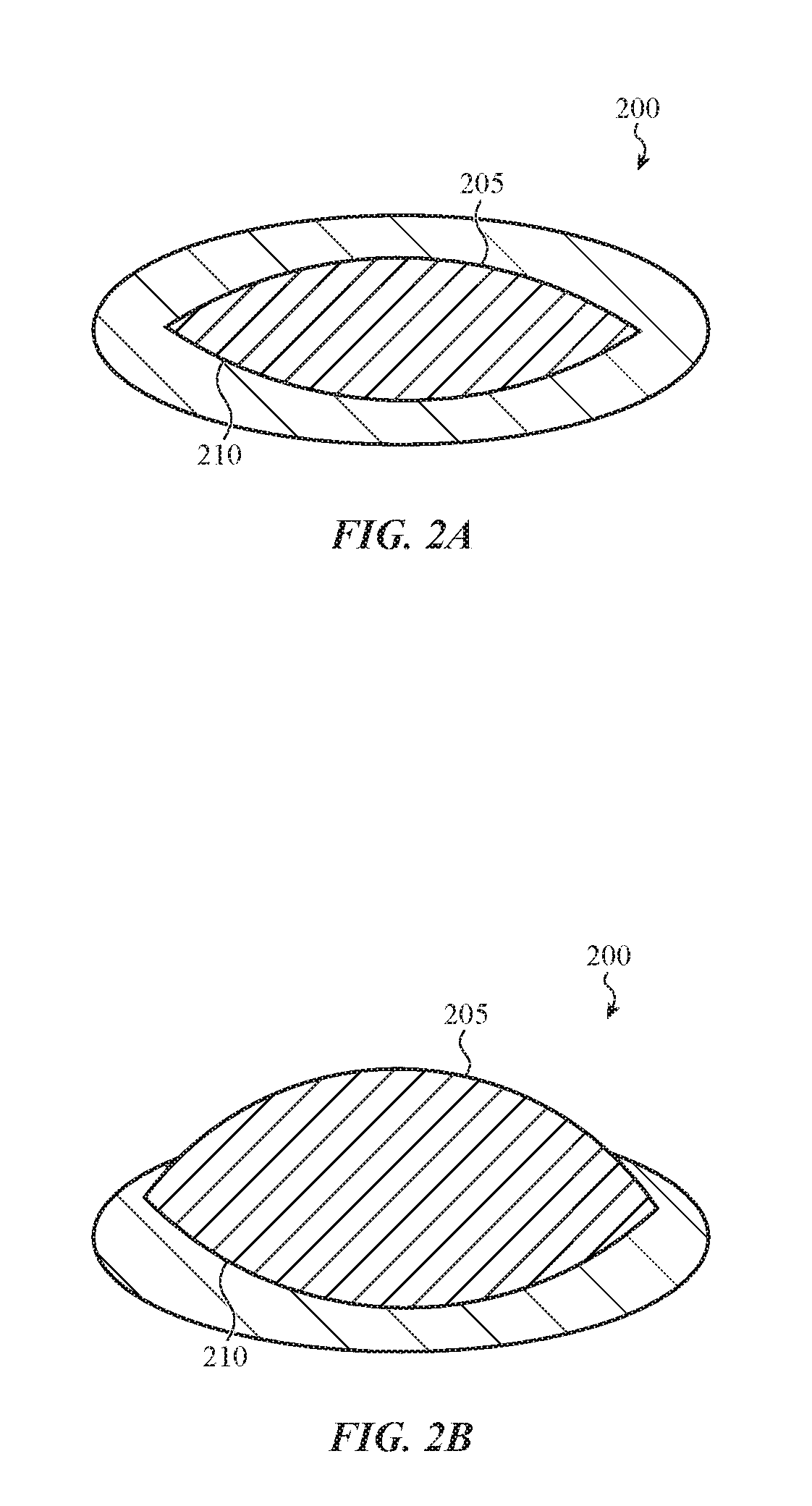
[0046] FIGS. 3A and 3B show a second anchoring configuration 300 for a piezoelectric body 305. FIG. 3A shows the piezoelectric body 305 in a non-energized state, and FIG. 3B shows the piezoelectric body 305 in an energized state.
[0047] In accordance with the second anchoring configuration 300, the piezoelectric body 305 may be clamped at two ends (e.g., two opposite ends 310, 315), and when actuated (energized) may bend up in the middle (as shown) or down (not shown). When not actuated (non-energized), and by way of example, the piezoelectric body 305 may take the form of a flat bar or sheet of material. The piezoelectric body 305 shown in FIGS. 3A and 3B may be referred to as a piezo bender, clamped on both ends.
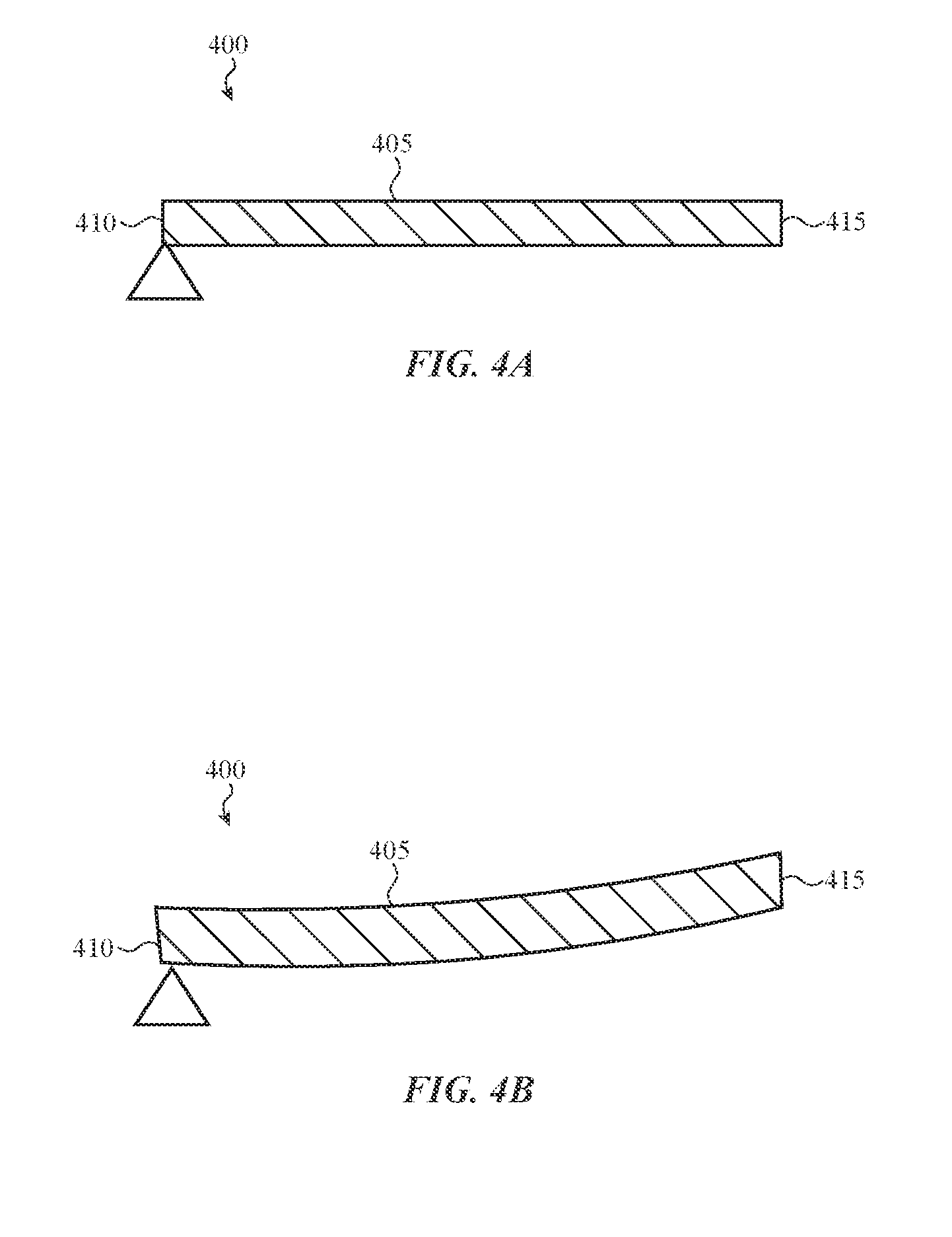
[0048] FIGS. 4A and 4B show a third anchoring configuration 400 for a piezoelectric body 405. FIG. 4A shows the piezoelectric body 405 in a non-energized state, and FIG. 4B shows the piezoelectric body 405 in an energized state.
[0049] In accordance with the third anchoring configuration 400, the piezoelectric body 405 may be clamped at one end 410, and when actuated (energized) may bend up or down at another end 415 (e.g., an opposite end). When not actuated (non-energized), and by way of example, the piezoelectric body 405 may take the form of a flat bar or sheet of material. The piezoelectric body 405 shown in FIGS. 4A and 4B may be referred to as a piezo bender, clamped on one end.
[0050] FIGS. 5A, 5B, and 5C show sample constructions of a piezoelectric body. The sample constructions may be employed in the haptic interface described with reference to FIG. 1, with any of the anchoring configurations described with reference to FIG. 2A, 2B, 3A, 3B, 4A, or 4B, or with other types of haptic interfaces or piezoelectric anchoring configurations.
[0051] FIG. 5A shows a unimorph construction of a piezoelectric body 500, in which a first layer 505 of piezoelectric material may be attached to a second layer 510 of non-piezoelectric material (e.g., a non-piezoelectric elastic material, such as a flex circuit). FIG. 5B shows a bimorph construction of a piezoelectric body 515, in which a first layer 520 of piezoelectric material may be attached to a second layer 525 of piezoelectric material. FIG. 5C shows a trimorph construction of a piezoelectric body 530, in which a first layer 535 of piezoelectric material is attached to one side of a layer 540 of non-piezoelectric material (e.g., a non-piezoelectric elastic material, such as a flex circuit), and a second layer 545 of piezoelectric material is attached to an opposite side of the layer 540 of non-piezoelectric material.
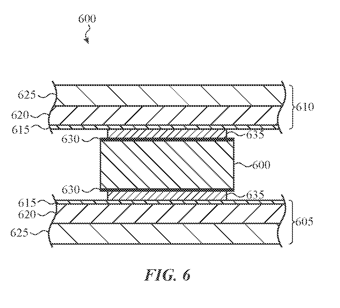
[0052] FIG. 6 shows a cross-section of a piezoelectric body 600 attached to first and second substrates 605, 610 (e.g., a bottom substrate 605 and a top substrate 610). As shown in FIG. 6, each of the first substrate 605 and the second substrate 610 may include multiple layers, such as a nickel (Ni) alloy layer 615, a copper (Cu) layer 620, and a platinum (Pl) layer 625. The copper layers 620 may include electrical conductors for routing signals between the piezoelectric body 600 and a circuit (e.g., a processor). The platinum layers 625 may act as stiffeners or ground shields for each substrate 605, 610. The nickel alloy layers 615 may provide conductive pads to which electrodes 630 attached to the piezoelectric body 600 may be bonded using a conductive adhesive 635 (e.g., an isotropic conductive film (ICF) or other conductive adhesive).
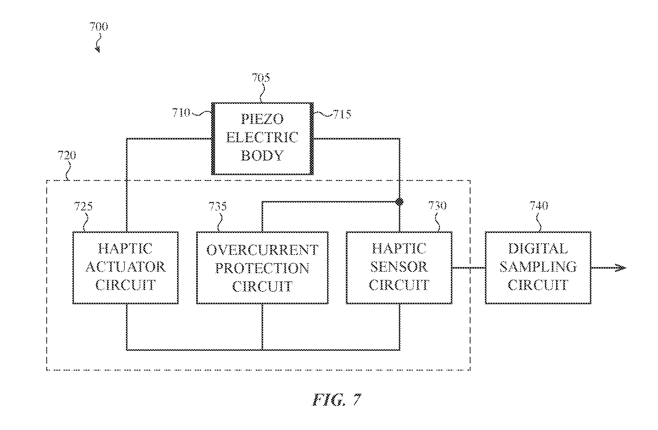
[0053] Referring to FIG. 7, there is shown a block diagram of a haptic interface 700 capable of providing a haptic output and sensing a haptic input. The haptic interface 700 may be an example of the haptic interface described with reference to FIG. 1.
[0054] The haptic interface 700 may include a piezoelectric body 705, first and second electrodes 710, 715 that are coupled to the piezoelectric body 705 to form a capacitor (C.sub.P), and a control circuit 720. The piezoelectric body 705 may take any of the forms described with reference to FIGS. 2-5, or other forms. In some embodiments, the piezoelectric body 705 may be configured as shown in FIG. 2A, 2B, 3A, 3B, 4A, 4B, 5A, 5B, 5C, or 6. The control circuit 720 may include a haptic actuator circuit 725 and a haptic sensor circuit 730. The haptic actuator circuit 725 may be coupled to the first electrode 710, and may be configured to charge the piezoelectric body 705 to provide a haptic output. The haptic sensor circuit 730 may be coupled to the second electrode 715, and may be configured to sense an electrical change at the second electrode 715. The electrical change may be a change in voltage, current, or charge, for example, and may be related to a haptic input (e.g., a force input) received by the piezoelectric body 705.
[0055] Optionally, the control circuit 720 may also include an overcurrent protection circuit 735. The overcurrent protection circuit 735 may be switchably operated (e.g., in response to a control signal) or automatically enabled (e.g., in response to an electrical change in the haptic interface 700) to limit a current flow into the haptic sensor circuit 730 while the haptic actuator circuit 725 is charging the piezoelectric body 705. The overcurrent protection circuit 735 may be needed to protect the haptic sensor circuit 730 because of one or more orders of magnitude difference between a haptic actuation signal provided by the haptic actuator circuit 725 to the piezoelectric body 705, to actuate the piezoelectric body 705, and a haptic input signal intended to be sensed by the haptic sensor circuit 730 (e.g., the haptic actuation signal may be one or more orders of magnitude greater than the haptic input signal).
[0056] A digital sampling circuit 740, such as an analog-to-digital converter (ADC), may be coupled to an output of the haptic sensor circuit 730.
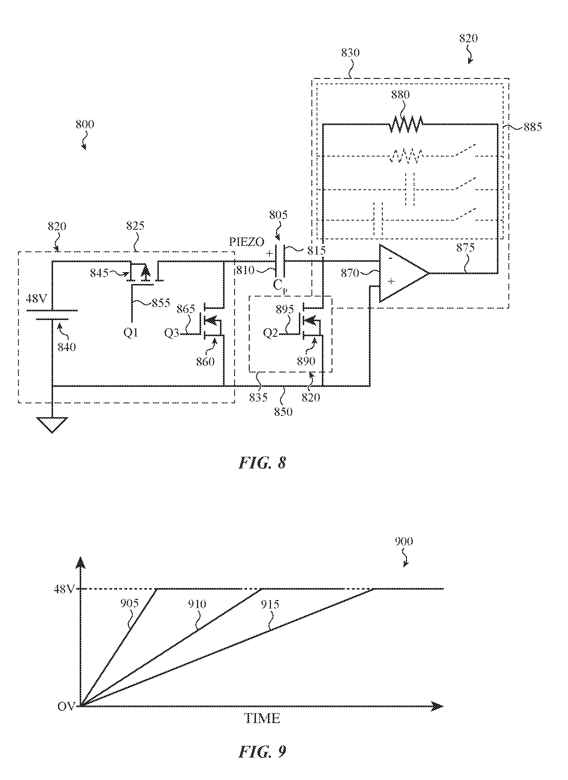
[0057] FIG. 8 shows a sample first circuit schematic 800 for a haptic interface, such as the haptic interface of FIG. 7. The haptic interface may include a piezoelectric body 805, a first electrode 810 coupled to the piezoelectric body 805, and a second electrode 815 coupled to the piezoelectric body 805. By way of example, the piezoelectric body 805 is depicted as a capacitor C.sub.P having a variable capacitance. In some cases, the piezoelectric body 805 may represent multiple piezoelectric bodies. The haptic interface may also include a control circuit 820. The control circuit 820 may include a haptic actuator circuit 825, a haptic sensor circuit 830, and an overcurrent protection circuit 835.
[0058] The haptic actuator circuit 825 may be coupled to the first electrode 810 and may be configured to charge the piezoelectric body 805. The charging may cause the piezoelectric body 805 to provide a haptic output (e.g., compress, deflect, deform, or otherwise physically change shape). The haptic sensor circuit 830 may be coupled to the second electrode 815 and may be configured to sense an electrical change (e.g., a change in voltage, change in current, or change in charge) at the second electrode 815. The electrical change may be related to a haptic input received by the piezoelectric body 805. The overcurrent protection circuit 835 may be coupled to the second electrode 815 and may be configured to limit a current flow into the haptic sensor circuit 830 while the haptic actuator circuit 825 is charging the piezoelectric body 805.
[0059] The haptic actuator circuit 825 may include a power source 840 and a first transistor 845, coupled in series between the first electrode 810 and a discharge node 850 (e.g., a ground). By way of example, the power source 840 is shown to be a 48V power source. In other embodiments, the power source 840 could supply a higher or lower voltage. The first transistor 845 may be coupled between the power source 840 and the first electrode 810 via its source and drain terminals, and may have a control input 855 (e.g., a gate input) configured to receive a signal that causes the first transistor 845 to open or close a current path between the first electrode 810 and the power source 840. The haptic actuator circuit 825 may also include a second transistor 860 coupled between the first electrode 810 and the discharge node 850. The second transistor 860 may be coupled between the first electrode 815 and the discharge node 850 via its source and drain terminals, and may have a control input 865 (e.g., a gate input) configured to receive a signal that causes the second transistor 860 to open or close a current path between the first electrode 810 and the discharge node 850.
[0060] The haptic sensor circuit 830 may include a sense amp 870 having a negative input coupled to the second electrode 815, a positive input coupled to the discharge node 850, and an output 875. A resistor 880 may be coupled between the negative input and the output 875. The configuration of the sense amp 870 is that of a transimpedance amplifier, which has no memory and can sense haptic input faster than certain other amplifier configurations. In some embodiments, the resistor 880 may be part of (or replaced by) a set of impedances 885. In some embodiments, the set of impedances 885 may include a number of resistors and capacitors connected in parallel. In some embodiments, one or more (or each) of the parallel-connected impedances may be connected in series with a switch. In these latter embodiments, the switches may be operated by the control circuit 820 to connect or disconnect impedances between the negative input and output 875 of the sense amp 870, thereby enabling the sense amp 870 to be operated in different modes (e.g., as a transimpedance amplifier or integrator).
[0061] The overcurrent protection circuit 835 may include a third transistor 890 coupled between the second electrode 810 and the discharge node 850, and also between the positive input and the negative input of the sense amp 870. The third transistor 890 may be coupled between the second electrode 815 and the discharge node 850 via its source and drain terminals, and may have a control input 895 (e.g., a gate input) configured to receive a signal that causes the third transistor 890 to open or close a current path between the second electrode 815 and the discharge node 850.
[0062] By way of example, the first, second, and third transistors 845, 860, 890 are shown to be N channel enhancement type metal oxide semiconductor field effect transistors (MOSFETs). In other examples, the transistors 845, 860, 890 may take other forms.
[0063] To charge the piezoelectric body 805 and provide a haptic output, the first transistor 845 may be closed and the second transistor 860 may be opened. While charging the piezoelectric body 805, the third transistor 890 may be closed to provide overcurrent protection for the haptic sensor circuit 830. In some cases, the third transistor 890 may be closed at the same time (and in some cases in response to the same control signal) as the first transistor 845. In other cases, the third transistor 890 may be closed prior to closing the first transistor 845. In still other cases, the third transistor 890 may be closed a predetermined time after closing the first transistor 845, or upon sensing a predetermined current flow into the haptic sensor circuit 830. If the piezoelectric body 805 is charged or discharged at a slow enough rate, the haptic sensor circuit 830 may monitor for haptic input to the piezoelectric body 805 during part or all of the charge time or discharge time. However, when the piezoelectric body 805 is charged or discharged quickly (which is considered typical), the haptic sensor circuit 830 may not monitor for haptic input to the piezoelectric body 805 during part or all of the charge time or discharge time (e.g., charging and sensing operations, or time periods, may be multiplexed).
[0064] To discharge the piezoelectric body 805, the second transistor 860 may be closed.
[0065] The haptic sensor circuit 830 may monitor for a haptic input to the piezoelectric body 805 by monitoring for an electrical change (e.g., a change in voltage, current, or charge) at the second electrode 815. To monitor for a haptic input, the third transistor 890 may be opened, while either (but not both) of the first and second transistors 845, 860 is closed. The haptic sensor circuit 830 may monitor for a haptic input during times when there is no charge on the piezoelectric body 805 (e.g., after the second transistor 860 has been closed and any charge on the piezoelectric body 805 has been discharged), or when there is a full charge on the piezoelectric body 805 (e.g., after the first transistor 845 has been closed and the piezoelectric body 805 has been fully charged).
[0066] FIG. 9 shows a graph 900 of voltage at the second electrode 815, over time, for various charging scenarios 905, 910, 915 of the piezoelectric body 805 shown in FIG. 8. Under each scenario 905, 910, 915, the voltage ramps up to a steady state high voltage (e.g., 48V). The slope of each charging ramp may determine an intensity of a haptic output. In the first and second scenarios 905, 910, a haptic input may be sensed at a steady state low voltage (e.g., 0V) and at the steady state high voltage, but not during charging of the piezoelectric body, because the rate of charging requires activation of the overcurrent protection circuit 835. In the third scenario 915, the charging ramp may be slow enough that the overcurrent protection circuit 835 does not need to be activated, and a haptic input may be sensed at the steady state low voltage, during charging, and at the steady state high voltage. In scenarios in which the overcurrent protection circuit 835 needs to be employed, the speed of recovering from overcurrent protection may determine the amount of haptic input information loss (e.g., during periods of overcurrent protection) and rate of haptic input information gathering.
[0067] FIG. 10 shows a sample second circuit schematic 1000 for a haptic interface, such as the haptic interface of FIG. 7. The haptic interface may include a piezoelectric body 1005, a first electrode 1010 coupled to the piezoelectric body 1005, and a second electrode 1015 coupled to the piezoelectric body 1005. By way of example, the piezoelectric body 1005 is depicted as a capacitor C.sub.P having a variable capacitance. In some cases, the piezoelectric body 1005 may represent multiple piezoelectric bodies. The haptic interface may also include a control circuit 1020. The control circuit 1020 may include a haptic actuator circuit 1025, a haptic sensor circuit 1030, and an overcurrent protection circuit 1035.
[0068] The haptic actuator circuit 1025 may be coupled to the first electrode 1010 and may be configured to charge the piezoelectric body 1005. The charging may cause the piezoelectric body 1005 to provide a haptic output (e.g., compress, deflect, deform, or otherwise physically change shape). The haptic sensor circuit 1030 may be coupled to the second electrode 1015 and may be configured to sense an electrical change (e.g., a change in voltage, change in current, or change in charge) at the second electrode 1015. The electrical change may be related to a haptic input received by the piezoelectric body 1005. The overcurrent protection circuit 1035 may be coupled to the second electrode 1015 and may be configured to limit a current flow into the haptic sensor circuit 1030 while the haptic actuator circuit 1025 is charging the piezoelectric body 1005.
[0069] The haptic actuator circuit 1025 may include a power source 1040 and a first transistor 1045, coupled in series between the first electrode 1010 and a discharge node 1050 (e.g., a ground). By way of example, the power source 1040 is shown to be a 48V power source. In other embodiments, the power source 1040 could supply a higher or lower voltage. The first transistor 1045 may be coupled between the power source 1040 and the first electrode 1010 via its source and drain terminals, and may have a control input 1055 (e.g., a gate input) configured to receive a signal that causes the first transistor 1045 to open or close a current path between the first electrode 1010 and the power source 1040. The haptic actuator circuit 1025 may also include a second transistor 1060 coupled between the first electrode 1010 and the discharge node 1050. The second transistor 1060 may be coupled between the first electrode 1010 and the discharge node 1050 via its source and drain terminals, and may have a control input 1065 (e.g., a gate input) configured to receive a signal that causes the second transistor 1060 to open or close a current path between the first electrode 1010 and the discharge node 1050.
[0070] The haptic sensor circuit 1030 may include a sense amp 1070 having a negative input coupled to the second electrode 1010, a positive input coupled to the discharge node 1050, and an output 1075. A resistor 1080 may be coupled between the negative input and the output 1075. The configuration of the sense amp 1070 is that of a transimpedance amplifier, which has no memory and can sense haptic input faster than certain other amplifier configurations. In some embodiments, the resistor 1080 may be part of (or replaced by) a set of impedances 1085. In some embodiments, the set of impedances 1085 may include a number of resistors and capacitors connected in parallel. In some embodiments, one or more (or each) of the parallel-connected impedances may be connected in series with a switch. In these latter embodiments, the switches may be operated by the control circuit 1020 to connect or disconnect impedances between the negative input and output 1075 of the sense amp 1070, thereby enabling the sense amp 1070 to be operated in different modes (e.g., as a transimpedance amplifier or integrator).
[0071] The overcurrent protection circuit 1035 may include a clamper circuit 1090 coupled between the second electrode 1015 and the discharge node 1050, and also between the positive input and the negative input of the sense amp 1070. The clamper circuit 1090 may include a forward-biased diode 1095 coupled in parallel with a reverse-biased diode 1098. Parameters of the diodes 1095, 1098 may be configured such that the clamper circuit 1090 automatically limits the current flow into the haptic sensor circuit 1030.
[0072] By way of example, the first and second transistors 1045, 1060 are shown to be N channel enhancement type MOSFETs. In other examples, the transistors 1045, 1060 may take other forms.
[0073] To charge the piezoelectric body 1005 and provide a haptic output, the first transistor 1045 may be closed and the second transistor 1060 may be opened. While charging the piezoelectric body 1005, the clamper circuit 1090 may automatically conduct to divert at least a portion of the current flow through the second electrode 1015 from into the haptic sensor circuit 1030 to the discharge node 1050, to provide overcurrent protection for the haptic sensor circuit 1030. For example, the clamper circuit 1090 may automatically conduct when the current flow (I.sub.CP) through the second electrode 1015 exceeds the maximum current (I.sub.opamp) supported by the sense amp 1070.
[0074] To discharge the piezoelectric body 1005, the second transistor 1060 may be closed.
[0075] When the clamper circuit 1090 is in an inactive state (e.g., when the piezoelectric body 1005 is charged to a steady-state high voltage or is at a steady-state low voltage), the haptic sensor circuit 1030 may monitor for a haptic input to the piezoelectric body 1005 by monitoring for an electrical change (e.g., a change in voltage, current, or charge) at the second electrode 1015. If the piezoelectric body 1005 is charged or discharged at a slow enough rate, the haptic sensor circuit 1030 may monitor for haptic input to the piezoelectric body 1005 during part or all of the charge time or discharge time. However, when the piezoelectric body 1005 is charged or discharged quickly (which is considered typical), the haptic sensor circuit 1030 may not monitor for haptic input to the piezoelectric body 1005 during part or all of the charge time or discharge time (e.g., charging and sensing operations, or time periods, may be multiplexed).
[0076] FIG. 11 shows a sample third circuit schematic 1100 for a haptic interface, such as the haptic interface of FIG. 7. The haptic interface may include a piezoelectric body 1105, a first electrode 1110 coupled to the piezoelectric body 1105, and a second electrode 1115 coupled to the piezoelectric body 1105. By way of example, the piezoelectric body 1105 is depicted as a capacitor C.sub.P having a variable capacitance. In some cases, the piezoelectric body 1105 may represent multiple piezoelectric bodies. The haptic interface may also include a control circuit 1120. The control circuit 1120 may include a haptic actuator circuit 1125, a haptic sensor circuit 1130, and an overcurrent protection circuit 1135.
[0077] The haptic actuator circuit 1125 may be coupled to the first electrode 1110 and may be configured to charge the piezoelectric body 1105. The charging may cause the piezoelectric body 1105 to provide a haptic output (e.g., compress, deflect, deform, or otherwise physically change shape). The haptic sensor circuit 1130 may be coupled to the second electrode 1115 and may be configured to sense an electrical change (e.g., a change in voltage, change in current, or change in charge) at the second electrode 1115. The electrical change may be related to a haptic input received by the piezoelectric body 1105. The overcurrent protection circuit 1135 may be coupled to the second electrode 1115, and may be configured to limit a current flow into the haptic sensor circuit 1130 while the haptic actuator circuit 1125 is charging the piezoelectric body 1105.
[0078] The haptic actuator circuit 1125 may include a power source 1140 coupled between the first electrode 1110 and a discharge node 1145 (e.g., a ground). By way of example, the power source 1140 is shown to be a 48V power source. In other embodiments, the power source 1140 could supply a higher or lower voltage. In contrast to the haptic interfaces described with reference to FIGS. 8 and 10, the haptic actuator circuit 1125 may maintain the piezoelectric body 1105 in a continually charged state.
[0079] The haptic sensor circuit 1130 may include a sense amp 1150 having a negative input coupled to the second electrode 1115, a positive input coupled to the discharge node 1145, and an output 1155. A resistor 1160 may be coupled between the negative input and the output 1155.
[0080] The overcurrent protection circuit 1135 may include a charge integration capacitor 1165 coupled between the second electrode 1115 and the output 1155 of the sense amp 1150. The charge integration capacitor 1165 may integrate charge leaked from the piezoelectric body 1105 over time. The charge integration capacitor 1165 may also be used to distinguish a force input to the piezoelectric body 1105 of short duration versus a force input of long duration. The charge on the charge integration capacitor 1165 may be periodically cleared (e.g., reset before performing a new sensing operation) by an integrated charge discharge circuit coupled to the charge integration capacitor 1165. The integrated charge discharge circuit may have a control input configured to receive a control signal that causes the integrated charge discharge circuit to discharge a charge integrated by the charge integration capacitor 1165.
[0081] FIG. 12 shows a sample fourth circuit schematic 1200 for a haptic interface, such as the haptic interface of FIG. 7. The haptic interface may include a piezoelectric body 1205, a first electrode 1210 coupled to the piezoelectric body 1205, and a second electrode 1215 coupled to the piezoelectric body 1205. By way of example, the piezoelectric body 1205 is depicted as a capacitor C.sub.P having a variable capacitance. In some cases, the piezoelectric body 1205 may represent multiple piezoelectric bodies. The haptic interface may also include a control circuit 1220. The control circuit 1220 may include a haptic actuator circuit 1225, a haptic sensor circuit 1230, and an overcurrent protection circuit 1235.
[0082] The haptic actuator circuit 1225 may be coupled to the first electrode 1210 and may be configured to charge the piezoelectric body 1205. The charging may cause the piezoelectric body 1205 to provide a haptic output (e.g., compress, deflect, deform, or otherwise physically change shape). The haptic sensor circuit 1230 may be coupled to the second electrode 1215 and may be configured to sense an electrical change (e.g., a change in voltage, change in current, or change in charge) at the second electrode 1215. The electrical change may be related to a haptic input received by the piezoelectric body 1205. The overcurrent protection circuit 1235 may be coupled to the second electrode 1215 and configured to limit a current flow into the haptic sensor circuit 1230 while the haptic actuator circuit 1225 is charging the piezoelectric body 1205.
[0083] The haptic actuator circuit 1225 may include a power source 1240 and a first transistor 1245, coupled in series between the first electrode 1210 and a discharge node 1250 (e.g., a ground). By way of example, the power source 1240 is shown to be a 48V power source. In other embodiments, the power source 1240 could supply a higher or lower voltage. The first transistor 1245 may be coupled between the power source 1240 and the first electrode 1210 via its source and drain terminals, and may have a control input 1255 (e.g., a gate input) configured to receive a signal that causes the first transistor 1245 to open or close a current path between the first electrode 1210 and the power source 1240. The haptic actuator circuit 1225 may also include a second transistor 1260 coupled between the first electrode 1210 and the discharge node 1250. The second transistor 1260 may be coupled between the first electrode 1210 and the discharge node 1250 via its source and drain terminals, and may have a control input 1265 (e.g., a gate input) configured to receive a signal that causes the second transistor 1260 to open or close a current path between the first electrode 1210 and the discharge node 1250.
[0084] The haptic sensor circuit 1230 may include a sense amp 1270 having a positive input coupled to the second electrode 1215, a negative input coupled to the discharge node 1250, and an output 1275.
[0085] The overcurrent protection circuit 1235 may include a third transistor 1280 coupled between the second electrode 1215 and the discharge node 1250, and also between the positive input and the negative input of the sense amp 1270. The third transistor 1280 may be coupled between the second electrode 1215 and the discharge node 1250 via its source and drain terminals, and may have a control input 1285 (e.g., a gate input) configured to receive a signal that causes the third transistor 1280 to open or close a current path between the second electrode 1215 and the discharge node 1250.
[0086] The first, second, and third transistors may take various forms.
[0087] To charge the piezoelectric body 1205 and provide a haptic output, the first transistor 1245 may be closed and the second transistor 1260 may be opened. While charging the piezoelectric body 1205, the third transistor 1280 may be closed to provide overcurrent protection for the haptic sensor circuit 1230. In some cases, the third transistor 1280 may be closed at the same time (and in some cases in response to the same control signal) as the first transistor 1245. In other cases, the third transistor 1280 may be closed prior to closing the first transistor 1245. In still other cases, the third transistor 1280 may be closed a predetermined time after closing the first transistor 1245, or upon sensing a predetermined current flow into the haptic sensor circuit 1230.
[0088] To discharge the piezoelectric body 1205, the second transistor 1260 may be closed.
[0089] The haptic sensor circuit 1230 may monitor for a haptic input to the piezoelectric body 1205 by monitoring for an electrical change (e.g., a change in voltage, current, or charge) at the second electrode 1215. To monitor for a haptic input, the third transistor 1280 may be opened, while either (but not both) of the first and second transistors 1245, 1260 is closed. The haptic sensor circuit 1230 may monitor for a haptic input during times when there is no charge on the piezoelectric body 1205 (e.g., after the second transistor 1260 has been closed and any charge on the piezoelectric body 1205 has been discharged), but not at times when there is a full charge on the piezoelectric body 1205 (e.g., after the first transistor 1245 has been closed and the piezoelectric body 1205 has been fully charged).
[0090] FIG. 13 shows a sample graph 1300 of voltage at the second electrode 1215, over time, for the piezoelectric body 1205 shown in FIG. 12. When charging the piezoelectric body 1205 to provide a haptic output (by asserting the .PHI..sub.1i control signal), the voltage ramps up to a steady state high voltage (e.g., 48V). After charging the piezoelectric body 1205, the piezoelectric body 1205 needs to be discharged (by asserting the .PHI..sub.2 control signal) before monitoring for a haptic input (e.g., at 0V).
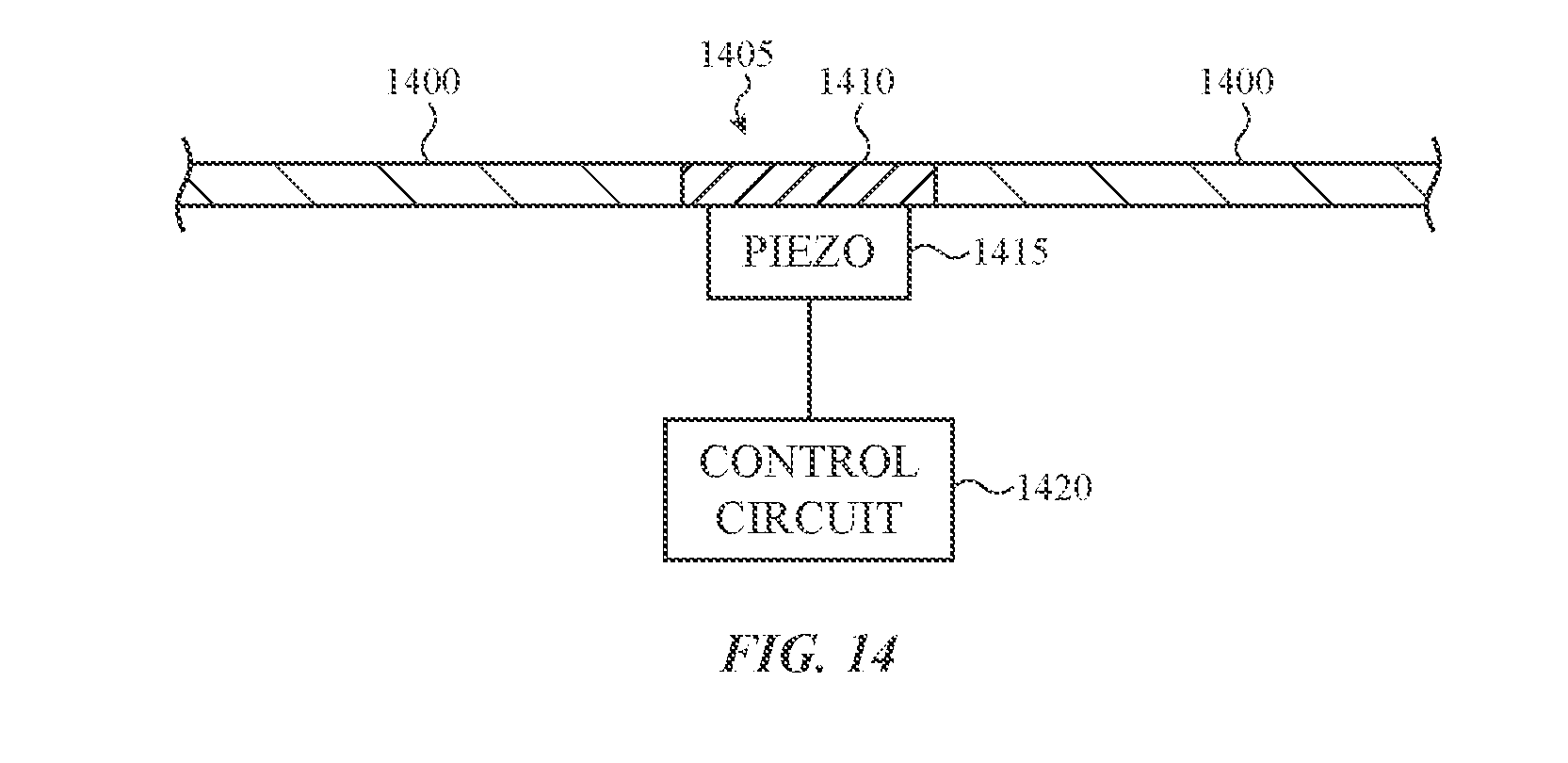
[0091] FIG. 14 shows a surface 1400 of an electronic device that may incorporate a haptic interface 1405 such as one of the haptic interfaces described with reference to FIG. 1, 7, 8, 10, 11, or 12. In some examples, the electronic device 1400 may be a smartphone, a tablet computer, or a wearable device (e.g., a watch).
[0092] In some embodiments, the surface 1400 may be part of a light-emitting display or a surface surrounding a light-emitting display. In some embodiments, the haptic interface 1405 may be part of a movable or generally immovable button 1410, which button 1410 has a fixed or movable (e.g., virtual) location on the surface 1400. In some embodiments, the haptic interface 1405 may be part of a keyboard (e.g., part of a key) on the surface 1400, which keyboard may be have movable or generally immovable keys. In some embodiments, the haptic interface 1405 may include a movable pin in place of the button 1410, or the button 1410 may include a movable pin (not shown). The haptic interface 1405 may include a piezoelectric body 1415, and a control circuit 1420 such as one of the control circuits described with reference to FIG. 8, 10, 11, or 12. The control circuit 1420 may configure the haptic interface 1405 as a haptic sensor (e.g., to sense a force input provided by a user of the electronic device), a haptic actuator (e.g., to provide a tactile output), or both simultaneously, as described in this disclosure. In some cases, the piezoelectric body 1415 may sense a force input while the piezoelectric body 1415 is charged or actuated and/or when the piezoelectric body 1415 is not charged or actuated.
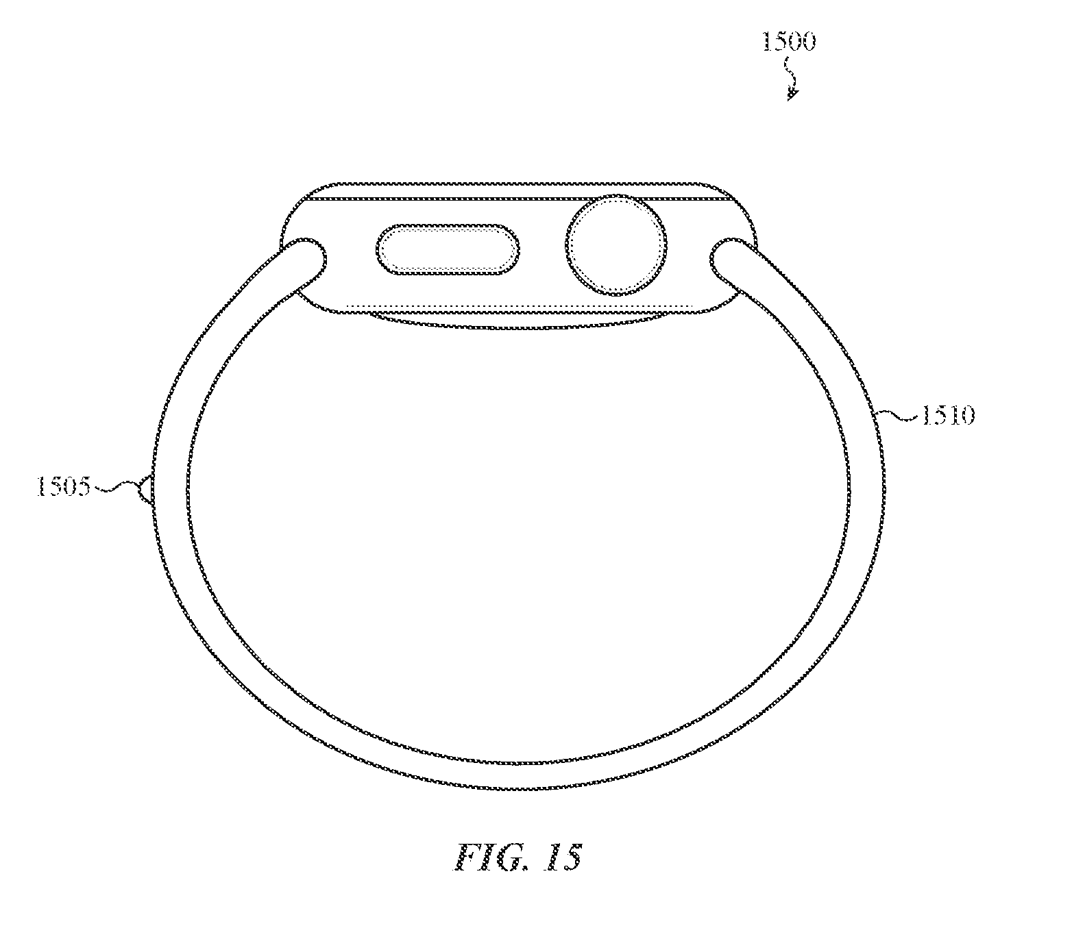
[0093] FIG. 15 shows an electronic device 1500 that may incorporate a haptic interface such as one of the haptic interfaces described with reference to FIG. 1, 7, 8, 10, 11, or 12. By way of example, the electronic device 1500 is shown to be a watch, though the electronic device 1500 could take other wearable forms or be a different type of electronic device (e.g., a non-wearable electronic device).
[0094] The electronic device 1500 may include a haptic interface 1505 that is usable by the electronic device 1500 as a notifier (e.g., an alarm or reminder) or presence sensor (e.g., a haptic prompt to inquiry whether a user is still engaged in an activity (e.g., exercising or performing a task) or still engaged with an application or utility running on the electronic device 1500 (e.g., a stopwatch utility)). In some examples, the haptic interface 1505 may include a piezoelectric body that is capable of providing a haptic output (e.g., a raised bump or pin). As shown, the haptic interface 1505 may be provided on an exterior surface of a smart watch band 1510. Alternatively, the haptic interface 1505 may be provided on an interior surface of the smart watch band 1510, or at another location on the electronic device 1500. In some examples, the piezoelectric body may be associated with one of the control circuits described with reference to FIG. 7, 8, 10, 11, or 12.
[0095] The haptic interface 1505 may sense a force input when it is actuated (e.g., when a piezoelectric body of the haptic interface 1505 is charged). In the case of an alarm or reminder, a user's force input to the haptic interface 1505 may cause the electronic device to clear the alarm or reminder (e.g., discharge a piezoelectric body or otherwise discontinue the haptic output).
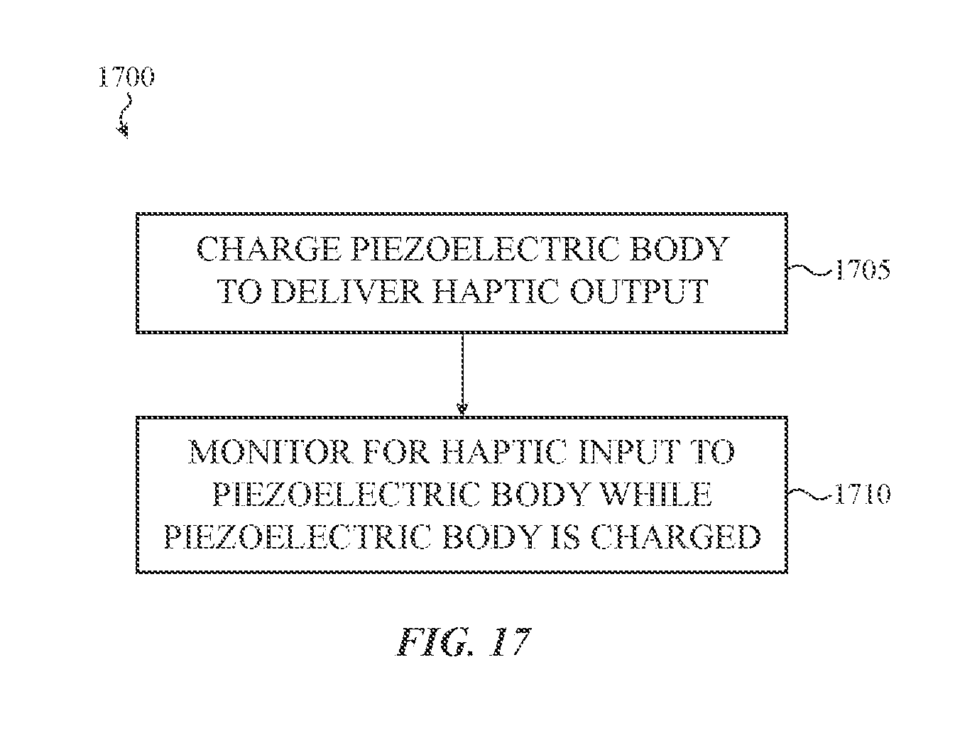
[0096] Referring now to FIG. 16, there is shown a method 1600 of operating a haptic interface. In some examples, the method 1600 may be performed by an electronic device, such as the electronic device described with reference to FIG. 1, 14, or 15.
[0097] At 1605, the method 1600 may include charging a piezoelectric body of the haptic interface to deliver a haptic output. The operation(s) at 1605 may be performed, for example, by the haptic actuator circuit described with reference to FIG. 8, 10, 11, or 12.
[0098] At 1610, the method 1600 may include limiting a current flow into a haptic sensor circuit while charging the piezoelectric body. The operation(s) at 1610 may be performed, for example, by the overprotection circuit described with reference to FIG. 8, 10, 11, or 12.
[0099] At 1615, the method 1600 may include monitoring for a haptic input to the piezoelectric body using the haptic sensor circuit while the piezoelectric body is charged. The operation(s) at 1615 may be performed, for example, by the haptic sensor circuit described with reference to FIG. 8, 10, 11, or 12.
[0100] In some examples, the method 1600 may include monitoring for a haptic input prior to charging the piezoelectric body and/or while charging the piezoelectric body.
[0101] In some examples, limiting the current flow into the haptic sensor circuit may include diverting at least a portion of the current flow from into the haptic sensor circuit to a discharge node. In some examples, diverting at least a portion of the current flow from into the haptic sensor circuit to the discharge node may include applying a control signal to a transistor. The transistor may be coupled between a first input and a second input of the haptic sensor circuit. Also, the first input may be coupled to an electrode attached to the piezoelectric body, and the second input may be coupled to the discharge node. In other examples, diverting at least a portion of the current flow from into the haptic sensor circuit to the discharge node may include automatically diverting at least the portion of the current flow based on a parameter of a diode.
[0102] In some examples, limiting the current flow into the haptic sensor circuit may include integrating a charge using a charge integrator (e.g., a capacitor) coupled between an input of the haptic sensor circuit and an output of the haptic sensor circuit, and clearing the integrated charge before monitoring for the haptic input.
[0103] FIG. 17 shows another method 1700 of operating a haptic interface. In some examples, the method 1700 may be performed by an electronic device, such as the electronic device described with reference to FIG. 1, 14, or 15.
[0104] At 1705, the method 1700 may include charging a piezoelectric body of the haptic interface to deliver a haptic output. The operation(s) at 1705 may be performed, for example, by the haptic actuator circuit described with reference to FIG. 8, 10, 11, or 12.
[0105] At 1710, the method 1700 may include monitoring for a haptic input to the piezoelectric body while the piezoelectric body is charged. The operation(s) at 1710 may be performed, for example, by the haptic sensor circuit described with reference to FIG. 8, 10, 11, or 12.
[0106] FIG. 18 shows a sample electrical block diagram of an electronic device 1800, which may be an example block diagram of the electronic device described with reference to FIG. 1, 14, or 15. The electronic device 1800 can include a display 1805 (e.g., a light-emitting display), a processor 1810, a power source 1815, a memory 1820 or storage device, a sensor 1825, an input/output (I/O) mechanism 1830 (e.g., an input/output device and/or input/output port), and a haptic interface 1835. The processor 1810 can control some or all of the operations of the electronic device 1800. The processor 1810 can communicate, either directly or indirectly, with substantially all of the components of the electronic device 100. For example, a system bus or other communication mechanism 1840 can provide communication between the processor 1810, the power source 1815, the memory 1820, the sensor 1825, the input/output mechanism 1830, and/or the haptic interface 1835.
[0107] The processor 1810 can be implemented as any electronic device capable of processing, receiving, or transmitting data or instructions. For example, the processor 1810 can be a microprocessor, a central processing unit (CPU), an application-specific integrated circuit (ASIC), a digital signal processor (DSP), or combinations of such devices. As described herein, the term "processor" is meant to encompass a single processor or processing unit, multiple processors, multiple processing units, or other suitably configured computing element or elements.
[0108] It should be noted that the components of the electronic device 1800 can be controlled by multiple processors. For example, select components of the electronic device 1800 may be controlled by a first processor and other components of the electronic device 1800 may be controlled by a second processor, where the first and second processors may or may not be in communication with each other.
[0109] The power source 1815 can be implemented with any device capable of providing energy to the electronic device 1800. For example, the power source 1815 may be one or more batteries or rechargeable batteries. Additionally or alternatively, the power source 1815 can be a power connector or power cord that connects the electronic device 1800 to another power source, such as a wall outlet.
[0110] The memory 1820 can store electronic data that can be used by the electronic device 1800. For example, the memory 1820 can store electrical data or content such as, for example, audio and video files, documents and applications, device settings and user preferences, timing signals, control signals, and data structures or databases. The memory 1820 can be configured as any type of memory. By way of example only, the memory 1820 can be implemented as random access memory, read-only memory, Flash memory, removable memory, other types of storage elements, or combinations of such devices.
[0111] The electronic device 1800 may also include one or more sensors 1825 positioned substantially anywhere on the electronic device 1800. The sensor(s) 1825 can be configured to sense substantially any type of characteristic, such as but not limited to, pressure, light, touch, heat, movement, relative motion, biometric data, and so on. For example, the sensor(s) 1825 may include a heat sensor, a position sensor, a light or optical sensor, an accelerometer, a pressure transducer, a gyroscope, a magnetometer, a health monitoring sensor, and so on. Additionally, the one or more sensors 1825 can utilize any suitable sensing technology, including, but not limited to, capacitive, ultrasonic, resistive, optical, ultrasound, piezoelectric, and thermal sensing technology.
[0112] The 110 mechanism 1830 can transmit and/or receive data from a user or another electronic device. An 110 device can include a display, a touch sensing input surface such as a track pad, one or more buttons (e.g., a graphical user interface "home" button), one or more cameras, one or more microphones or speakers, one or more ports such as a microphone port, and/or a keyboard. Additionally or alternatively, an 110 device or port can transmit electronic signals via a communications network, such as a wireless and/or wired network connection. Examples of wireless and wired network connections include, but are not limited to, cellular, Wi-Fi, Bluetooth, IR, and Ethernet connections.
[0113] The haptic interface 1835 may be operably connected to the processor 1810, display 1805, or other components of the electronic device 1800. The haptic interface 1835 may provide the processor 1810 a signal corresponding to compression, deflection, deformation, or other movement of one or more piezoelectric bodies of the haptic interface 1835, and the processor 1810 may wake up a portion of the electronic device 1800, manipulate a graphical element on the display 1805 of the electronic device 1800, or perform another operation in response to the signal. The processor 1810 may also activate the haptic interface 1835 to solicit a user's attention, enhance the user's interaction experience with the electronic device 1800, displace the electronic device 1800 or a component of the electronic device 1800, or provide any other suitable notification or user experience. The haptic interface 1835 may be activated, for example, by generating a signal that causes one or more piezoelectric bodies of the haptic interface 1835 to compress, deflect, deform, or otherwise physically change. The haptic interface 1835 may also function as a sensor 1825, and may receive force input from a user of the electronic device 1800.
[0114] The foregoing description, for purposes of explanation, uses specific nomenclature to provide a thorough understanding of the described embodiments. However, it will be apparent to one skilled in the art that the specific details are not required in order to practice the described embodiments. Thus, the foregoing descriptions of the specific embodiments described herein are presented for purposes of illustration and description. They are not targeted to be exhaustive or to limit the embodiments to the precise forms disclosed. It will be apparent to one of ordinary skill in the art that many modifications and variations are possible in view of the above teachings.
* * * * *
D00000
D00001
D00002
D00003
D00004
D00005
D00006
D00007
D00008
D00009
D00010
D00011
D00012
D00013

D00014
D00015
XML
uspto.report is an independent third-party trademark research tool that is not affiliated, endorsed, or sponsored by the United States Patent and Trademark Office (USPTO) or any other governmental organization. The information provided by uspto.report is based on publicly available data at the time of writing and is intended for informational purposes only.
While we strive to provide accurate and up-to-date information, we do not guarantee the accuracy, completeness, reliability, or suitability of the information displayed on this site. The use of this site is at your own risk. Any reliance you place on such information is therefore strictly at your own risk.
All official trademark data, including owner information, should be verified by visiting the official USPTO website at www.uspto.gov. This site is not intended to replace professional legal advice and should not be used as a substitute for consulting with a legal professional who is knowledgeable about trademark law.