Photonic Integrated Circuit Edge Coupler Structure With Reduced Reflection For Integrated Laser Diodes
Sayyah; Keyvan ; et al.
U.S. patent application number 16/019686 was filed with the patent office on 2019-01-17 for photonic integrated circuit edge coupler structure with reduced reflection for integrated laser diodes. The applicant listed for this patent is GM GLOBAL TECHNOLOGY OPERATIONS LLC. Invention is credited to Oleg Efimov, Biqin Huang, Pamela R. Patterson, Raymond Sarkissian, Keyvan Sayyah.
| Application Number | 20190018198 16/019686 |
| Document ID | / |
| Family ID | 64998803 |
| Filed Date | 2019-01-17 |


| United States Patent Application | 20190018198 |
| Kind Code | A1 |
| Sayyah; Keyvan ; et al. | January 17, 2019 |
PHOTONIC INTEGRATED CIRCUIT EDGE COUPLER STRUCTURE WITH REDUCED REFLECTION FOR INTEGRATED LASER DIODES
Abstract
A photonic chip, an edge coupler for an integrated photonic system and a method for coupling a laser to the photonic chip. The edge coupler includes a waveguide of the photonic system having a longitudinal axis. The longitudinal axis of a waveguide of the photonic chip is aligned with a longitudinal axis of the laser. The facet of the waveguide facing the laser is at a non-perpendicular angle with respect to the longitudinal axis. Light is transmitted from the laser into the waveguide via the angled facet.
| Inventors: | Sayyah; Keyvan; (Santa Monica, CA) ; Efimov; Oleg; (Thousand Oaks, CA) ; Patterson; Pamela R.; (Los Angeles, CA) ; Sarkissian; Raymond; (Studio City, CA) ; Huang; Biqin; (Torrance, CA) | ||||||||||
| Applicant: |
|
||||||||||
|---|---|---|---|---|---|---|---|---|---|---|---|
| Family ID: | 64998803 | ||||||||||
| Appl. No.: | 16/019686 | ||||||||||
| Filed: | June 27, 2018 |
Related U.S. Patent Documents
| Application Number | Filing Date | Patent Number | ||
|---|---|---|---|---|
| 62531414 | Jul 12, 2017 | |||
| Current U.S. Class: | 1/1 |
| Current CPC Class: | G01S 17/42 20130101; H01S 5/125 20130101; H01L 2223/54486 20130101; B81B 7/02 20130101; H01L 2223/54426 20130101; G01S 7/491 20130101; G02B 2006/0098 20130101; G01S 7/4818 20130101; G01S 7/4972 20130101; G01S 7/4817 20130101; G01S 17/32 20130101; G01S 7/4913 20130101; G02B 6/2766 20130101; H01L 23/544 20130101; G01S 7/4816 20130101; G01S 17/34 20200101; G01S 17/86 20200101; G01S 7/4914 20130101; H01L 31/16 20130101; G01S 7/4815 20130101; G01S 7/4911 20130101; G01S 17/58 20130101; G01S 17/02 20130101; B81B 2207/03 20130101; G02B 6/4209 20130101; G01S 17/003 20130101; G01S 17/931 20200101; G02B 6/122 20130101; G02B 27/30 20130101; G01S 7/499 20130101; H01L 31/02327 20130101 |
| International Class: | G02B 6/35 20060101 G02B006/35; G02B 6/122 20060101 G02B006/122; G01S 17/02 20060101 G01S017/02; G01S 7/491 20060101 G01S007/491; G01S 7/481 20060101 G01S007/481 |
Claims
1. An edge coupler for an integrated photonic system, comprising: a waveguide of the photonic system having a longitudinal axis; and a facet at an end of the waveguide for optical communication with a laser, wherein the facet is at a non-perpendicular angle with respect to the longitudinal axis.
2. The edge coupler of claim 1, wherein the waveguide further comprises an outer waveguide surrounding an inner waveguide, wherein light entering the outer waveguide via the facet is transmitted via the inner waveguide.
3. The edge coupler of claim 2, wherein the inner waveguide includes a facet located a selected distance from the facet of the outer waveguide.
4. The edge coupler of claim 3, wherein the facet of the inner waveguide is perpendicular to the longitudinal axis.
5. The edge coupler of claim 3, wherein an end of the inner waveguide having the facet tapers to reduce the width of the inner waveguide in a direction approaching the facet.
6. The edge coupler of claim 2, wherein the inner waveguide is made of Silicon and the outer waveguide is made of SiON.
7. The edge coupler of claim 1, wherein the angle optimizes light coupling between the laser and the waveguide and minimizes back reflection into the laser.
8. The edge coupler of claim 1, wherein a longitudinal axis of a laser is collinear with the longitudinal axis of the waveguide.
9. A method for coupling a laser to a photonic chip, comprising: aligning a longitudinal axis of a waveguide of the photonic chip with a longitudinal axis of the laser, wherein a facet of the waveguide facing the laser is at a non-perpendicular angle with respect to the longitudinal axis; and transmitting light from the laser into the waveguide via the angled facet.
10. The method of claim 9, wherein the waveguide further comprises an outer waveguide surrounding an inner waveguide, further comprising transmitting the light to enter the outer waveguide via the facet, wherein the light is transmitted to the photonic chip via the inner waveguide.
11. The method of claim 10, wherein the inner waveguide includes a facet located at a selected distance from the facet of the outer waveguide.
12. The method of claim 11, wherein the facet of the inner waveguide is perpendicular to the longitudinal axis.
13. The method of claim 12, wherein a section of the inner waveguide proximate the facet of the inner waveguide tapers to reduce the width of the inner waveguide in a direction approaching the facet.
14. The method of claim 10, wherein the inner waveguide is made of Silicon and the outer waveguide is made of SiON.
15. The method of claim 9, wherein the angle optimizes light coupling between the laser and the waveguide and minimizes back reflection into the laser.
16. The method of claim 9, wherein a longitudinal axis of the laser is collinear with the longitudinal axis of the waveguide.
17. A photonic chip, comprising: a waveguide having a longitudinal axis; and a facet at an end of the waveguide for optical communication with a laser, wherein the facet is at a non-perpendicular angle with respect to the longitudinal axis.
18. The photonic chip of claim 17, wherein the waveguide further comprises an outer waveguide surrounding an inner waveguide, wherein light enters the outer waveguide via the facet is transmitted via the inner waveguide.
19. The photonic chip of claim 18, wherein the inner waveguide includes a facet located a selected distance from the facet of the outer waveguide, the facet of the inner waveguide being perpendicular to the longitudinal axis, and wherein the inner waveguide includes a section proximate the facet of the inner waveguide that tapers to reduce the width of the inner waveguide in a direction approaching the facet.
20. The photonic chip of claim 17, wherein the angle is selected to optimize light coupling between the laser and the waveguide and to minimize back reflection into the laser.
Description
CROSS-REFERENCE TO RELATED APPLICATIONS
[0001] This application claims the benefit of priority of U.S. Provisional Application No. 62/531,414 filed Jul. 12, 2017, the disclosure of which is incorporated herein by reference in its entirety.
INTRODUCTION
[0002] The subject disclosure relates to a method and apparatus for of coupling a laser beam to a photonic chip and, in particular, to reducing back-reflection at a coupling between the laser beam and the photonic chip.
[0003] A chip-based LIDAR (Light Detection and Ranging) system includes a photonic chip that uses a laser to generate light. Light from the laser enters into the photonic chip in order to pass through various systems of the photonic chip. An edge coupler is used to receive the light from the laser. However, light can be back-reflected at the edge coupler, which can degrade the linewidth and single frequency operation of the laser. In addition, such back-reflection reduces the intensity of light usable for LIDAR purposes. Accordingly, it is desirable to provide an edge coupler for the photonic chip that reduces an amount of back-reflection that can be coupled into the laser cavity.
SUMMARY
[0004] In one exemplary embodiment, an edge coupler for an integrated photonic system is disclosed. The edge coupler includes a waveguide of the photonic system having a longitudinal axis, and a facet at an end of the waveguide for optical communication with a laser. The facet is at a non-perpendicular angle with respect to the longitudinal axis.
[0005] In addition to one or more of the features described herein, the waveguide further includes an outer waveguide surrounding an inner waveguide, and the light entering the outer waveguide via the facet is transmitted via the inner waveguide. The inner waveguide includes a facet located a selected distance from the facet of the outer waveguide. The facet of the inner waveguide is perpendicular to the longitudinal axis. An end of the inner waveguide having the facet tapers to reduce the width of the inner waveguide in a direction approaching the facet. In various embodiments, the inner waveguide is made of Silicon and the outer waveguide is made of SiON. The angle of the facet of the waveguide is selected to optimize light coupling between the laser and the waveguide and to minimize back reflection into the laser. A longitudinal axis of a laser is made collinear with the longitudinal axis of the waveguide.
[0006] In another exemplary embodiment, a method for coupling a laser to a photonic chip is disclosed. The method includes aligning a longitudinal axis of a waveguide of the photonic chip with a longitudinal axis of the laser, wherein a facet of the waveguide facing the laser is at a non-perpendicular angle with respect to the longitudinal axis, and transmitting light from the laser into the waveguide via the angled facet.
[0007] In addition to one or more of the features described herein, the waveguide further includes an outer waveguide surrounding an inner waveguide, further comprising transmitting the light to enter the outer waveguide via the facet, wherein the light is transmitted to the photonic chip via the inner waveguide. The inner waveguide includes a facet located at a selected distance from the facet of the outer waveguide. The facet of the inner waveguide is perpendicular to the longitudinal axis. A section of the inner waveguide proximate the facet of the inner waveguide tapers to reduce the width of the inner waveguide in a direction approaching the facet. In various embodiments, the inner waveguide is made of Silicon and the outer waveguide is made of SiON. The angle optimizes light coupling between the laser and the waveguide and minimizes back reflection into the laser. A longitudinal axis of the laser is made collinear with the longitudinal axis of the waveguide.
[0008] In yet another exemplary embodiment, a photonic chip is disclosed. The photonic chip includes a waveguide having a longitudinal axis, and a facet at an end of the waveguide for optical communication with a laser. The facet is at a non-perpendicular angle with respect to the longitudinal axis.
[0009] In addition to one or more of the features described herein, the waveguide further includes an outer waveguide surrounding an inner waveguide, wherein light enters the outer waveguide via the facet is transmitted via the inner waveguide. The inner waveguide includes a facet located a selected distance from the facet of the outer waveguide, the facet of the inner waveguide being perpendicular to the longitudinal axis. The inner waveguide includes a section proximate the facet of the inner waveguide that tapers to reduce the width of the inner waveguide in a direction approaching the facet. The angle is selected to optimize light coupling between the laser and the waveguide and to minimize back reflection into the laser.
[0010] The above features and advantages, and other features and advantages of the disclosure are readily apparent from the following detailed description when taken in connection with the accompanying drawings.
BRIEF DESCRIPTION OF THE DRAWINGS
[0011] Other features, advantages and details appear, by way of example only, in the following detailed description, the detailed description referring to the drawings in which:
[0012] FIG. 1 shows a schematic diagram of a LIDAR system;
[0013] FIG. 2 shows an exemplary photonic chip suitable for use in the LIDAR system of FIG. 1; and
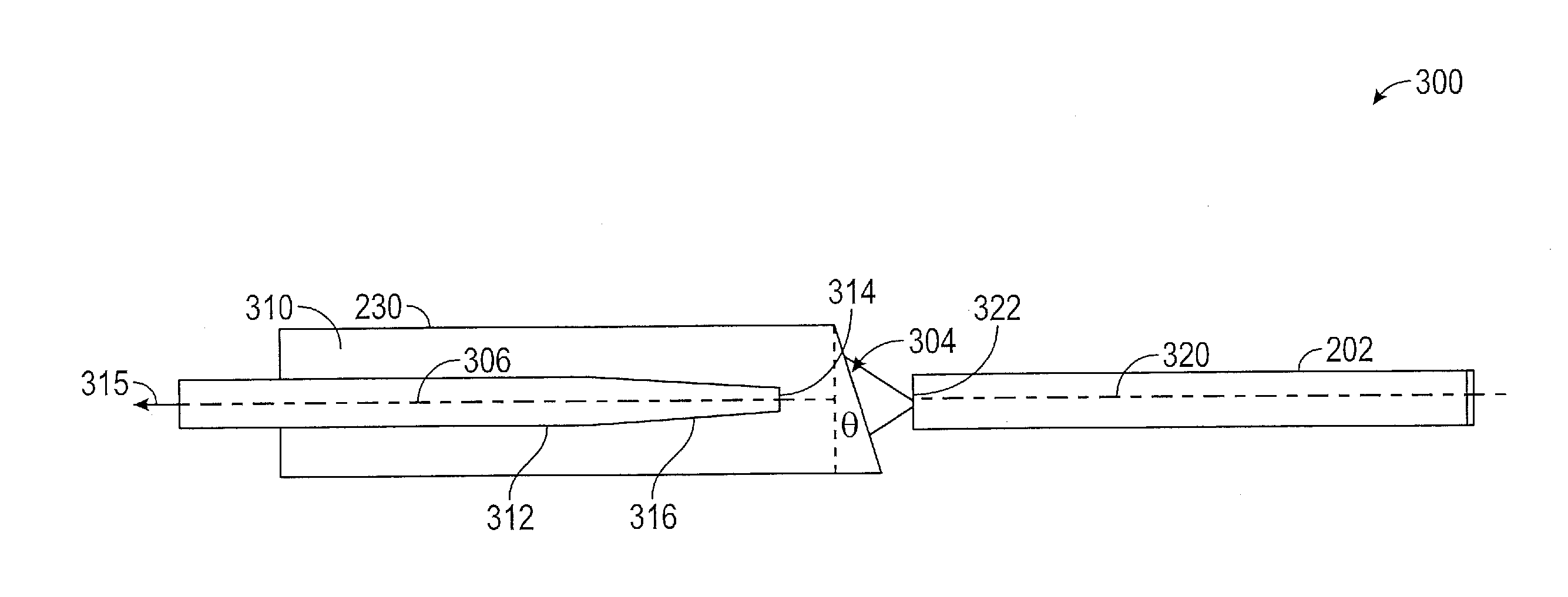
[0014] FIG. 3 shows an arrangement of a laser and an edge coupler for maximizing an amount of light transmitted from the laser into the edge coupler while reducing or minimizing an amount of light backscattered into the laser.
DETAILED DESCRIPTION
[0015] The following description is merely exemplary in nature and is not intended to limit the present disclosure, its application or uses. It should be understood that throughout the drawings, corresponding reference numerals indicate like or corresponding parts and features.
[0016] In accordance with an exemplary embodiment, FIG. 1 shows a schematic diagram of a LIDAR system 100. The LIDAR system 100 includes a photonic chip 102, an optical coupler 104, and a microelectromechanical system (MEMS) scanner 106. A processor 108 controls operation of the photonic chip 102 in order to perform operations of the LIDAR system 100. In various embodiments, the LIDAR system 100 are disposed on a semiconductor integrated chip residing on a printed circuit board. As discussed in further detail with respect to FIG. 2, the photonic chip 102 includes a light source, such as a laser, an optical waveguiding network and a set of photodiodes. The laser generates a transmitted light beam 115 that is transmitted toward an object 110. Reflected light beam 117, which is due to interaction of the object 110 is optically mixed with a fraction (<10%) of the transmitted light beam 115, in a set of photodiodes. The processor 108 controls the operation of the light source by controlling a waveform that modulates the light source. The processor 108 further receives data from the photodiodes and determines various parameters of an object 110 from the data.
[0017] In operation, the processor 108 controls the light source of the photonic chip 102 to generate a modulated transmitted beam of light 115. The transmitted beam of light 115 passes through the optical coupler 104 which collimates the transmitted light beam 115 and directs the transmitted light beam 115 toward the MEMS scanner 106. The MEMS scanner 106 steers the transmitted light beam 115 over a range of angles into a surrounding region of the LIDAR system 100.
[0018] The MEMS scanner 106 includes a vibrating member such as a vibrating mirror. The processor 108 controls an oscillation of the vibrating member in order to steer the transmitted light beam 115 over a selected range of angles. In various embodiments, the MEMS scanner 106 is a two-dimensional (2D) MEMS scanner, and the processor 108 controls oscillation of the vibration member in two angular direction, such as azimuth and elevation.
[0019] Reflected light beam 117 is formed when object 110 interacts with the transmitted light beam 115. A portion of the reflected light beam 117 is received at the MEMS scanner 106. The MEMS scanner 106 directs the reflected light beam 117 into the optical coupler 104 which focuses the reflected light beam 117 into the photonic chip 102.
[0020] In various embodiments, the LIDAR 100 system can be associated with a vehicle and the object 110 can be any object external to the vehicle, such as another vehicle, a pedestrian, a telephone pole, etc. The LIDAR system 100 determines parameters such as range, and Doppler as a function of the azimuth and elevation of the object 110 and the vehicle uses these parameters to navigate with respect to the object 110 for the purposes of avoiding contact with the object 110.
[0021] FIG. 2 shows an exemplary photonic chip 102 suitable for use in the LIDAR system 100 of FIG. 1. In various embodiments, the photonic chip 102 is a scanning frequency modulated continuous wave (FMCW) LIDAR chip. The photonic chip 102 can be a silicon photonic chip in various embodiments. The photonic chip 102 receives light from a coherent light source such as a laser 202. The laser 202 can be independent from the photonic chip 102 or can be an integrated component of the photonic chip 102. The laser 202 can be any single frequency laser which can be frequency modulated. In an embodiment, the laser 202 is a distributed Bragg reflector laser. In various embodiments, the laser 202 generates light at a frequency of 1550 nanometers (nm) or other wavelength considered safe to human eyes. The laser 202 is coupled to a transmitter waveguide 204 via an edge coupler 230 that receives the light from the laser 202. The transmitter waveguide 204 directs the light from the laser 202 out of the photonic chip 102 via a transmitter beam edge or grating coupler 220 as transmitted light beam 115.
[0022] A local oscillator (LO) waveguide 206 is optically coupled to the transmitter waveguide 204 via a directional coupler/splitter or a multi-mode interference coupler/splitter 210 located between the light source 202 and the edge coupler 220. The directional coupler/splitter or the multi-mode interference coupler/splitter 210 splits the light from the laser 202 into a transmitted light beam 115 that continues to propagate in the transmitter waveguide 204 and a local oscillator beam that propagates in the local oscillator waveguide 206. In various embodiments, a splitting ratio can be 90% for the transmitter beam and 10% for the local oscillator beam. The local oscillator beam is directed toward a dual-balanced photodetector 214 that performs beam measurements.
[0023] Incoming or reflected light beam 117 enters the receiver waveguide 208 via a receiver beam edge or grating coupler 222. The receiver waveguide 208 directs the reflected light beam 117 from the receiver beam edge or grating coupler 222 to the dual-balanced photodetector 214. The receiver waveguide 208 is optically coupled to the local oscillator waveguide 206 at a directional coupler/combiner or multi-mode interference coupler/combiner 212 located between the edge or grating coupler 222 and the photodetector 214. The local oscillator beam and the reflected light beam 117 therefore interact with each other at the directional coupler/combiner or multi-mode interference coupler/combiner 212 before being received at the dual-balanced photodetector 214. In various embodiments, the transmitter waveguide 204, local oscillator waveguide 206 and receiver waveguide 208 can be optical fibers.
[0024] The dual-balanced photodetector 214 detects the frequency difference between in the transmitted light beam 115 and the reflected light beam 117 due to reflection of the transmitter beam off of object 110, FIG. 1. The dual-balanced photodetector 214 is coupled to processor 108, FIG. 1. The processor 108, FIG. 1 determines, from the frequency differences, parameters of the object 110, such as range or distance, a direction of arrival of the object 110, and a velocity of the object 110 relative to the LIDAR system 100.
[0025] FIG. 3 shows an arrangement 300 of a laser 202 and an edge coupler 230 for maximizing an amount of light transmitted from the laser 202 into the edge coupler 230 while reducing or minimizing an amount of light backscattered into the laser 202. In various embodiments, the edge coupler 230 is a cylindrical waveguide, such as an optical fiber. The edge coupler 230 includes a longitudinal axis 306 and a facet 304 at an end of the edge coupler 230 facing the laser 202. A longitudinal axis 320 of the laser 202 is aligned or substantially aligned with the longitudinal axis 306 of the waveguide 230.
[0026] The edge coupler 230 includes an edge coupler waveguide 310 and a photonic integrated circuit (PIC) waveguide 312 in an interior of an edge coupler waveguide 310. The edge coupler waveguide 310 therefore is an outer waveguide to the inner waveguide of the PIC waveguide 312. The PIC waveguide 312 is made of a first material while the edge coupler waveguide 310 is made of a second material. A longitudinal axis 315 of the PIC waveguide 312 is collinear or substantially collinear with the longitudinal axis 306 of the edge coupler waveguide 310. The PIC waveguide 312 and the edge coupler waveguide 310 are optical waveguides. The edge coupler waveguide 310 includes a facet 304 at an end facing the laser 202. The facet 304 is at an angle 0 that makes the facet 304 non-perpendicular to the longitudinal axis 306 of the edge coupler waveguide 310 and thus non-perpendicular to the longitudinal axis 320 of the laser 202 (i.e., facet 304 is non-parallel to facet 322 of laser 202).
[0027] Having the facet of the edge coupler waveguide 310 at a non-perpendicular angle to the longitudinal 320 axis reduces an amount of back-reflection of light back into the laser 202. Also, when the angle 0 of the edge coupler facet 304 an optimum angle, a maximum light coupling occurs between the laser 202 and the edge coupler 230 simultaneous with minimum back-reflection into the laser 202.
[0028] The PIC waveguide 312 includes a tapered end 316. The tapered end 316 is a selected distance from the facet 304 of the edge coupler waveguide 310. The facet 314 of the PIC waveguide 312 is perpendicular to the longitudinal axis and the tapered end 316 of the PIC waveguide 312 tapers to reduce the diameter, radius or width of the PIC waveguide 312 in the direction traveling toward the facet 314.
[0029] Any light that is reflected from the edge coupler waveguide 310 is directed at the laser output facet 322 at an angle off of the longitudinal axes 306, 320 and hence does not disturb the laser operation. The PIC waveguide 312 captures the laser light and directs the light to a location of the integrated circuit.
[0030] While the above disclosure has been described with reference to exemplary embodiments, it will be understood by those skilled in the art that various changes may be made and equivalents may be substituted for elements thereof without departing from its scope. In addition, many modifications may be made to adapt a particular situation or material to the teachings of the disclosure without departing from the essential scope thereof. Therefore, it is intended that the present disclosure not be limited to the particular embodiments disclosed, but will include all embodiments falling within the scope thereof.
* * * * *
D00000
D00001
D00002
D00003
XML
uspto.report is an independent third-party trademark research tool that is not affiliated, endorsed, or sponsored by the United States Patent and Trademark Office (USPTO) or any other governmental organization. The information provided by uspto.report is based on publicly available data at the time of writing and is intended for informational purposes only.
While we strive to provide accurate and up-to-date information, we do not guarantee the accuracy, completeness, reliability, or suitability of the information displayed on this site. The use of this site is at your own risk. Any reliance you place on such information is therefore strictly at your own risk.
All official trademark data, including owner information, should be verified by visiting the official USPTO website at www.uspto.gov. This site is not intended to replace professional legal advice and should not be used as a substitute for consulting with a legal professional who is knowledgeable about trademark law.