3d Semiconductor Device And Structure
Or-Bach; Zvi ; et al.
U.S. patent application number 16/101489 was filed with the patent office on 2019-01-03 for 3d semiconductor device and structure. This patent application is currently assigned to Monolithic 3D Inc.. The applicant listed for this patent is Monolithic 3D Inc.. Invention is credited to Brian Cronquist, Zvi Or-Bach, Deepak C. Sekar, Zeev Wurman.
| Application Number | 20190006222 16/101489 |
| Document ID | / |
| Family ID | 64734986 |
| Filed Date | 2019-01-03 |


View All Diagrams
| United States Patent Application | 20190006222 |
| Kind Code | A1 |
| Or-Bach; Zvi ; et al. | January 3, 2019 |
3D SEMICONDUCTOR DEVICE AND STRUCTURE
Abstract
A 3D semiconductor device, including: a first level including a single crystal layer, a plurality of first transistors, and a first metal layer, forming memory control circuits; a second level overlaying the single crystal layer, and including a plurality of second transistors and a plurality of first memory cells; a third level overlaying the second level, and including a plurality of third transistors and a plurality of second memory cells; where the second transistors are aligned to the first transistors with less than 40 nm alignment error, where the memory cells include a NAND non-volatile memory type, where some of the memory control circuits can control at least one of the memory cells, and where some of the memory control circuits are designed to perform a verify read after a write pulse so to detect if the at least one of the memory cells has been successfully written.
| Inventors: | Or-Bach; Zvi; (San Jose, CA) ; Cronquist; Brian; (San Jose, CA) ; Sekar; Deepak C.; (San Jose, CA) ; Wurman; Zeev; (Palo Alto, CA) | ||||||||||
| Applicant: |
|
||||||||||
|---|---|---|---|---|---|---|---|---|---|---|---|
| Assignee: | Monolithic 3D Inc. San Jose CA |
||||||||||
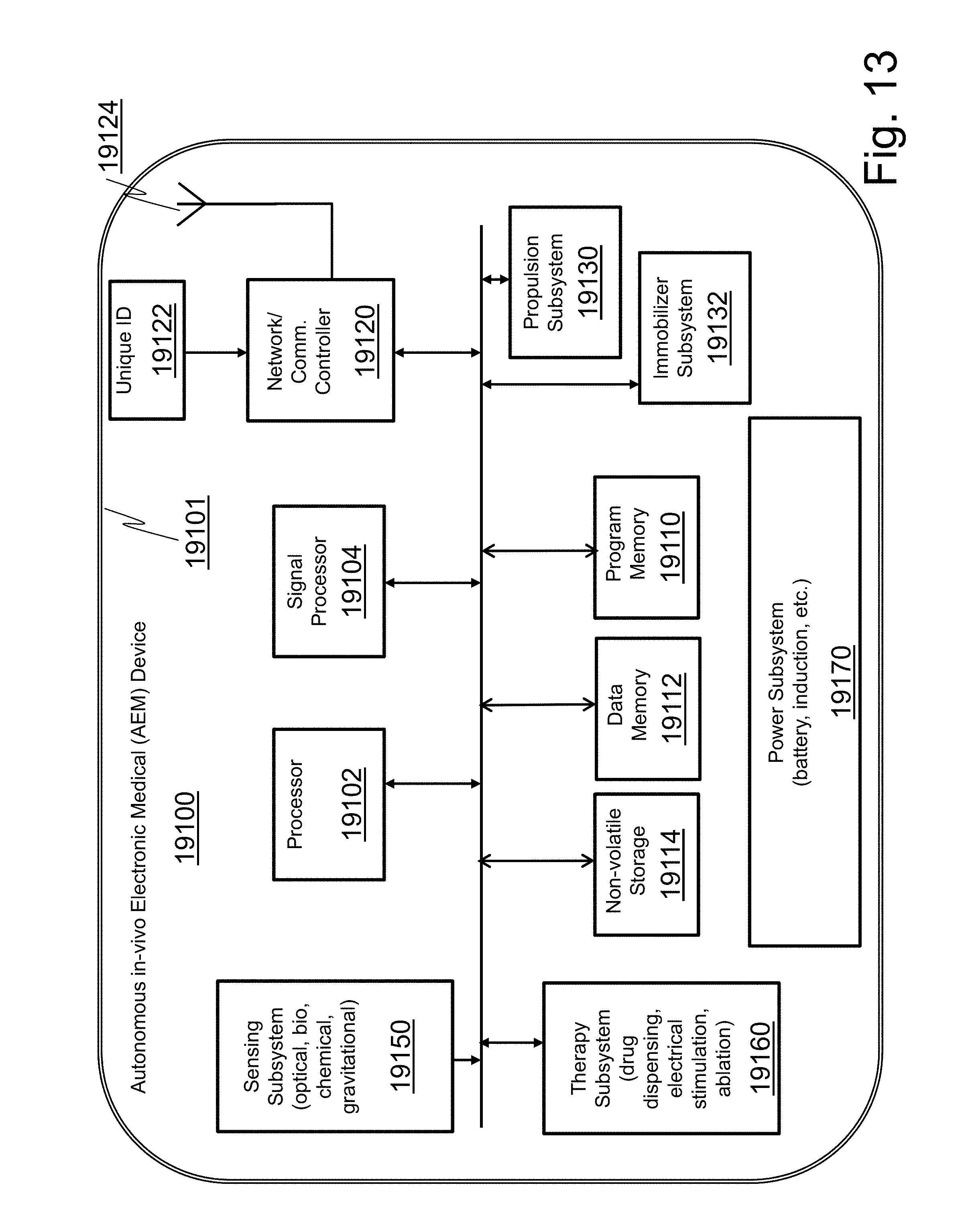
| Family ID: | 64734986 | ||||||||||
| Appl. No.: | 16/101489 | ||||||||||
| Filed: | August 12, 2018 |
Related U.S. Patent Documents
| Application Number | Filing Date | Patent Number | ||
|---|---|---|---|---|
| 15460230 | Mar 16, 2017 | |||
| 16101489 | ||||
| 14821683 | Aug 7, 2015 | 9613844 | ||
| 15460230 | ||||
| 13492395 | Jun 8, 2012 | 9136153 | ||
| 14821683 | ||||
| 13273712 | Oct 14, 2011 | 8273610 | ||
| 13492395 | ||||
| 13016313 | Jan 28, 2011 | 8362482 | ||
| 13273712 | ||||
| 12970602 | Dec 16, 2010 | 9711407 | ||
| 13016313 | ||||
| 12949617 | Nov 18, 2010 | 8754533 | ||
| 12970602 | ||||
| Current U.S. Class: | 1/1 |
| Current CPC Class: | H01L 21/6835 20130101; H01L 23/481 20130101; H01L 27/11 20130101; H01L 29/66621 20130101; H01L 29/775 20130101; H01L 2224/32225 20130101; H01L 2924/1579 20130101; H01L 23/3677 20130101; H01L 27/11551 20130101; H01L 29/7881 20130101; H01L 2924/01046 20130101; H01L 2924/1305 20130101; H01L 27/10897 20130101; H01L 29/792 20130101; H01L 2924/12036 20130101; H01L 2924/3011 20130101; H01L 27/11807 20130101; H01L 29/42392 20130101; H01L 29/66272 20130101; H01L 2221/68368 20130101; H01L 2924/12042 20130101; H01L 2924/30105 20130101; H01L 29/66439 20130101; H01L 2224/16225 20130101; H01L 2224/45147 20130101; H01L 2224/73265 20130101; H01L 2924/01066 20130101; H01L 2924/01078 20130101; H01L 27/10802 20130101; H01L 28/00 20130101; H01L 29/66825 20130101; H01L 45/04 20130101; H01L 2224/32145 20130101; H01L 2224/83894 20130101; H01L 2924/13062 20130101; H01L 2924/1431 20130101; H01L 2924/1461 20130101; H01L 2225/06558 20130101; H01L 2224/45124 20130101; H01L 2924/13091 20130101; H01L 2223/5442 20130101; H01L 2924/00014 20130101; H01L 25/50 20130101; H01L 27/11578 20130101; H01L 29/7371 20130101; H01L 2924/12033 20130101; H01L 27/1266 20130101; H01L 2924/1434 20130101; H01L 27/11529 20130101; H01L 27/0688 20130101; H01L 29/7841 20130101; H01L 45/1226 20130101; H01L 2924/01013 20130101; H01L 2924/1301 20130101; H01L 2924/14 20130101; H01L 27/10873 20130101; H01L 23/544 20130101; H01L 27/10894 20130101; H01L 2224/16145 20130101; H01L 27/10 20130101; H01L 29/4236 20130101; H01L 2225/06513 20130101; H01L 2924/01019 20130101; H01L 2224/16227 20130101; H01L 27/11898 20130101; H01L 27/1207 20130101; H01L 2223/54453 20130101; H01L 23/5252 20130101; H01L 25/0655 20130101; H01L 27/11526 20130101; H01L 45/146 20130101; H01L 2223/54426 20130101; H01L 2924/3025 20130101; H01L 29/78 20130101; H01L 2224/80001 20130101; H01L 2924/181 20130101; H01L 2924/00015 20130101; H01L 2924/01002 20130101; H01L 2924/01068 20130101; H01L 2224/73253 20130101; H01L 2924/01018 20130101; H01L 21/76254 20130101; H01L 21/76898 20130101; H01L 2224/16146 20130101; H01L 21/8221 20130101; H01L 21/823828 20130101; H01L 27/105 20130101; H01L 2924/10253 20130101; H01L 2924/16152 20130101; H01L 27/092 20130101; H01L 27/112 20130101; H01L 27/11206 20130101; H01L 29/0673 20130101; H01L 2224/16235 20130101; H01L 21/823475 20130101; H01L 2924/00011 20130101; H01L 2924/01004 20130101; H01L 2924/19041 20130101; G11C 8/16 20130101; H01L 27/088 20130101; H01L 29/7855 20130101; H01L 2924/01322 20130101; H01L 24/13 20130101; H01L 27/11573 20130101; H01L 29/785 20130101; H01L 21/84 20130101; H01L 27/10876 20130101; H01L 29/7843 20130101; H01L 29/78696 20130101; H01L 2224/81005 20130101; H01L 2924/00012 20130101; H01L 2924/01077 20130101; H01L 2924/12032 20130101; H01L 2924/15311 20130101; H01L 25/0657 20130101; H01L 27/1108 20130101; H01L 29/66545 20130101; H01L 2225/06541 20130101; H01L 29/66833 20130101; H01L 21/743 20130101; H01L 27/0207 20130101; H01L 27/1214 20130101; H01L 2924/01029 20130101; H01L 27/1203 20130101; H01L 29/732 20130101; H01L 2224/131 20130101; H01L 2924/00 20130101; H01L 2924/014 20130101; H01L 2224/73204 20130101; H01L 27/2436 20130101; H01L 2924/10329 20130101; H01L 24/16 20130101; H01L 27/249 20130101; H01L 29/66901 20130101; H01L 2224/48091 20130101; H01L 2924/00014 20130101; H01L 2224/131 20130101; H01L 2924/014 20130101; H01L 2224/73265 20130101; H01L 2224/32225 20130101; H01L 2224/48227 20130101; H01L 2924/00015 20130101; H01L 2224/73265 20130101; H01L 2224/32145 20130101; H01L 2224/48227 20130101; H01L 2924/00015 20130101; H01L 2924/16152 20130101; H01L 2224/73253 20130101; H01L 2224/32225 20130101; H01L 2224/48227 20130101; H01L 2924/00 20130101; H01L 2924/15311 20130101; H01L 2224/73265 20130101; H01L 2224/32225 20130101; H01L 2224/48227 20130101; H01L 2924/00 20130101; H01L 2924/10253 20130101; H01L 2924/00 20130101; H01L 2924/1301 20130101; H01L 2924/00 20130101; H01L 2924/1461 20130101; H01L 2924/00 20130101; H01L 2924/12032 20130101; H01L 2924/00 20130101; H01L 2924/1305 20130101; H01L 2924/00 20130101; H01L 2924/13062 20130101; H01L 2924/00 20130101; H01L 2924/00011 20130101; H01L 2224/80001 20130101; H01L 2224/45124 20130101; H01L 2924/00014 20130101; H01L 2224/45147 20130101; H01L 2924/00014 20130101; H01L 2924/12033 20130101; H01L 2924/00 20130101; H01L 2924/12036 20130101; H01L 2924/00 20130101; H01L 2224/73204 20130101; H01L 2224/16225 20130101; H01L 2224/32225 20130101; H01L 2924/00 20130101; H01L 2924/12042 20130101; H01L 2924/00 20130101; H01L 2924/15311 20130101; H01L 2224/73204 20130101; H01L 2224/16225 20130101; H01L 2224/32225 20130101; H01L 2924/00 20130101; H01L 2924/00014 20130101; H01L 2224/05599 20130101; H01L 2224/131 20130101; H01L 2924/014 20130101; H01L 2924/00014 20130101; H01L 2224/73204 20130101; H01L 2224/16145 20130101; H01L 2224/32145 20130101; H01L 2924/00 20130101 |
| International Class: | H01L 21/683 20060101 H01L021/683; H01L 29/792 20060101 H01L029/792; G11C 8/16 20060101 G11C008/16; H01L 29/78 20060101 H01L029/78; H01L 29/66 20060101 H01L029/66; H01L 29/423 20060101 H01L029/423; H01L 27/12 20060101 H01L027/12; H01L 27/118 20060101 H01L027/118; H01L 27/11578 20170101 H01L027/11578; H01L 27/11573 20170101 H01L027/11573; H01L 27/11551 20170101 H01L027/11551; H01L 27/11529 20170101 H01L027/11529; H01L 27/11526 20170101 H01L027/11526; H01L 27/112 20060101 H01L027/112; H01L 27/11 20060101 H01L027/11; H01L 27/108 20060101 H01L027/108; H01L 27/105 20060101 H01L027/105; H01L 27/10 20060101 H01L027/10; H01L 27/092 20060101 H01L027/092; H01L 27/06 20060101 H01L027/06; H01L 27/02 20060101 H01L027/02; H01L 23/525 20060101 H01L023/525; H01L 23/48 20060101 H01L023/48; H01L 21/84 20060101 H01L021/84; H01L 21/8238 20060101 H01L021/8238; H01L 21/822 20060101 H01L021/822; H01L 21/768 20060101 H01L021/768; H01L 21/762 20060101 H01L021/762; H01L 21/74 20060101 H01L021/74; H01L 29/788 20060101 H01L029/788 |
Claims
1. A 3D semiconductor device, the device comprising: a first level comprising a single crystal layer, a plurality of first transistors, a plurality of first contact plugs and a first metal layer, wherein connections between said first transistors and first metal layer comprise said first contact plugs; memory control circuits comprising a portion of said connections and said plurality of first transistors; a second level overlaying said single crystal layer, said second level comprising a plurality of second transistors; a third level overlaying said second level, said third level comprising a plurality of third transistors; a second metal layer overlaying said third level; and a third metal layer overlaying said second metal layer, wherein said second transistors are aligned to said first transistors with less than 40 nm alignment error, wherein said third metal layer comprises bit lines, wherein said second level comprises a plurality of first memory cells, wherein said third level comprises a plurality of second memory cells, wherein one of said second transistors is at least partially self-aligned to at least one of said third transistors, wherein at least one of said second memory cells comprises at least one of said third transistors, wherein said memory cells comprise a NAND non-volatile memory type, wherein said second transistors channel and source or drain comprise a similar doping type, wherein at least one of said memory control circuits is designed to control at least one of said memory cells, and wherein at least a portion of said memory control circuits are designed to perform a verify read after a write pulse so to detect if said at least one of said memory cells has been successfully written.
2. The 3D semiconductor device according to claim 1, further comprising: a connective path from one of said second transistors to one of said first transistors, wherein said path comprises a through-layer via, and wherein said through-layer via has a diameter of less than 400 nm.
3. The 3D semiconductor device according to claim 1, wherein at least one of said second transistors comprises a polysilicon transistor channel.
4. The 3D semiconductor device according to claim 1, wherein said perform comprises adjusting a write voltage according to a result of said verify read.
5. The 3D semiconductor device according to claim 1, wherein at least one of said second transistors partially overlays at least a portion of said memory control circuits.
6. The 3D semiconductor device according to claim 1, further comprising: a first set of external connections underlying said first layer to connect said device to a first external device; and a second set of external connections overlying said third metal layer to connect said device to a second external device, wherein said first set of external connections comprises a through silicon via (TSV).
7. The 3D semiconductor device according to claim 1, wherein at least one of said second transistors overlays at least a portion of said first metal layer.
8. A 3D semiconductor device, the device comprising: a first level comprising a single crystal layer, a plurality of first transistors, a plurality of first contact plugs and a first metal layer, wherein connections between said first transistors and first metal layer comprise said first contact plugs; memory control circuits comprising a portion of said connections and said plurality of first transistors; a second level overlaying said single crystal layer, said second level comprising a plurality of second transistors; a third level overlaying said second level, said third level comprising a plurality of third transistors; a second metal layer overlaying said third level; and a third metal layer overlaying said second metal layer, wherein said second transistors are aligned to said first transistors with less than 40 nm alignment error, wherein said third metal layer comprises bit lines, wherein said second level comprises a plurality of first memory cells, wherein said third level comprises a plurality of second memory cells, wherein one of said second transistors is at least partially self-aligned to at least one of said third transistors, wherein at least one of said second memory cells comprises at least one of said third transistors, wherein said memory cells comprise a NAND non-volatile memory type, and wherein at least a portion of said memory control circuits are designed to perform a verify read after a write pulse so to detect if said at least one of said memory cells has been successfully written.
9. The 3D semiconductor device according to claim 8, and further comprising: a connective path from one of said second transistors to one of said first transistors, wherein said path comprises a through-layer via, and wherein said through-layer via has a diameter of less than 400 nm.
10. The 3D semiconductor device according to claim 8, wherein at least one of said second transistors comprises a polysilicon transistor channel.
11. The 3D semiconductor device according to claim 8, wherein said perform comprises adjusting a write voltage according to a result of said verify read.
12. The 3D semiconductor device according to claim 8, wherein said second transistors channel and source or drain comprise a similar doping type.
13. The 3D semiconductor device according to claim 8, wherein at least one of said second transistors at least partially overlays at least one of said first transistors.
14. The 3D semiconductor device according to claim 1, further comprising: a first set of external connections underlying said first layer to connect said device to a first external device; and a second set of external connections overlying said third metal layer to connect said device to a second external device, wherein said first set of external connections comprises a through silicon via (TSV).
15. A 3D semiconductor device, the device comprising: a first level comprising a single crystal layer, a plurality of first transistors, a plurality of first contact plugs and a first metal layer, wherein connections between said first transistors and first metal layer comprise said first contact plugs; memory control circuits comprising a portion of said connections and said plurality of first transistors; a second level overlaying said single crystal layer, said second level comprising a plurality of second transistors; a third level overlaying said second level, said third level comprising a plurality of third transistors; a second metal layer overlaying said third level; and a third metal layer overlaying said second metal layer, wherein said second transistors are aligned to said first transistors with less than 40 nm alignment error, wherein said second level comprises a plurality of first memory cells, wherein said third level comprises a plurality of second memory cells, and wherein at least a portion of said memory control circuits are designed to perform a verify read after a write pulse so to detect if said at least one of said memory cells has been successfully written.
16. The 3D semiconductor device according to claim 15, wherein at least one of said third transistors comprises a polysilicon transistor channel.
17. The 3D semiconductor device according to claim 15, wherein at least one of said third transistors is a junction-less transistor.
18. The 3D semiconductor device according to claim 15, wherein one of said second transistors is at least partially self-aligned to at least one of said third transistors.
19. The 3D semiconductor device according to claim 15, wherein at least one of said memory cells comprises at least one of said third transistors.
20. The 3D semiconductor device according to claim 15, further comprising: a connective path from one of said second transistors to one of said first transistors, wherein said path comprises a through-layer via, and wherein said through-layer via has a diameter of less than 400 nm.
Description
CROSS-REFERENCE OF RELATED APPLICATION
Background of the Invention
1. Field of the Invention
[0001] This application relates to the general field of Integrated Circuit (IC) devices and fabrication methods, and more particularly to multilayer or Three Dimensional Integrated Circuit (3D IC) devices and fabrication methods.
SUMMARY
[0002] The invention may be directed to multilayer or Three Dimensional Integrated Circuit (3D IC) devices and fabrication methods.
[0003] In one aspect, a 3D semiconductor device, the device comprising: a first level comprising a single crystal layer, a plurality of first transistors, a plurality of first contact plugs and a first metal layer, wherein said first contact plugs comprise connections between said first transistors and first metal layer, forming memory control circuits; a second level overlaying said single crystal layer, said second level comprising a plurality of second transistors; a third level overlaying said second level, said third level comprising a plurality of third transistors; a second metal layer overlaying said third level; and a third metal layer overlaying said second metal layer, wherein said second transistors are aligned to said first transistors with less than 40 nm alignment error, wherein said third metal layer comprises bit lines, wherein said second level comprises a plurality of first memory cells, wherein said third level comprises a plurality of second memory cells, wherein one of said second transistors is at least partially self-aligned to at least one of said third transistors, wherein at least one of said second memory cells comprises at least one of said third transistors, wherein said memory cells comprise a NAND non-volatile memory type, wherein said second transistors channel and source or drain comprise a similar doping type, wherein at least one of said memory control circuits is designed to control at least one of said memory cells, and wherein at least a portion of said memory control circuits are designed to perform a verify read after a write pulse so to detect if said at least one of said memory cells has been successfully written.
[0004] In another aspect, a 3D semiconductor device, the device comprising: a first level comprising a single crystal layer, a plurality of first transistors, a plurality of first contact plugs and a first metal layer, wherein said first contact plugs comprise connections between said first transistors and first metal layer, forming memory control circuits; a second level overlaying said single crystal layer, said second level comprising a plurality of second transistors; a third level overlaying said second level, said third level comprising a plurality of third transistors; a second metal layer overlaying said third level; and a third metal layer overlaying said second metal layer, wherein said second transistors are aligned to said first transistors with less than 40 nm alignment error, wherein said third metal layer comprises bit lines, wherein said second level comprises a plurality of first memory cells, wherein said third level comprises a plurality of second memory cells, wherein one of said second transistors is at least partially self-aligned to at least one of said third transistors, wherein at least one of said second memory cells comprises at least one of said third transistors, wherein said memory cells comprise a NAND non-volatile memory type, and wherein at least a portion of said memory control circuits are designed to perform a verify read after a write pulse so to detect if said at least one of said memory cells has been successfully written; a connective path from one of said second transistors to one of said first transistors, wherein said path comprises a through-layer via, and wherein said through-layer via has a diameter of less than 400 nm.
[0005] In another aspect, a 3D semiconductor device, the device comprising: a first level comprising a single crystal layer, a plurality of first transistors, a plurality of first contact plugs and a first metal layer, wherein said first contact plugs comprise connections between said first transistors and first metal layer, forming memory control circuits; a second level overlaying said single crystal layer, said second level comprising a plurality of second transistors; a third level overlaying said second level, said third level comprising a plurality of third transistors; a second metal layer overlaying said third level; and a third metal layer overlaying said second metal layer, wherein said second transistors are aligned to said first transistors with less than 40 nm alignment error, wherein said second level comprises a plurality of first memory cells, wherein said third level comprises a plurality of second memory cells, and wherein at least a portion of said memory control circuits are designed to perform a verify read after a write pulse so to detect if said at least one of said memory cells has been successfully written, and wherein at least one of said third transistors comprises a polysilicon transistor channel.
BRIEF DESCRIPTION OF THE DRAWINGS
[0006] Various embodiments of the invention will be understood and appreciated more fully from the following detailed description, taken in conjunction with the drawings in which:
[0007] FIG. 1 is an exemplary drawing illustration of a 3D integrated circuit;
[0008] FIG. 2 is an exemplary drawing illustration of another 3D integrated circuit;
[0009] FIG. 3 is an exemplary drawing illustration of the power distribution network of a 3D integrated circuit;
[0010] FIG. 4 is an exemplary drawing illustration of a NAND gate;
[0011] FIG. 5 is an exemplary drawing illustration of the thermal contact concept;
[0012] FIG. 6 is an exemplary drawing illustration of the use of heat spreaders in 3D stacked device layers;
[0013] FIGS. 7A-7B are exemplary drawing illustrations of the use and retention of thermally conductive hard mask layers for patterning contact layers of 3D stacked device layers;
[0014] FIG. 8A is an exemplary drawing illustration of a 4 input NAND gate;
[0015] FIG. 8B is an exemplary drawing illustration of a 4 input NAND gate where all parts of the logic cell can be within desirable temperature limits;
[0016] FIG. 9 is an exemplary procedure for a chip designer to ensure a good thermal profile for a design;
[0017] FIG. 10A is an exemplary drawing illustration of chamfering the custom function etching shape for stress relief;
[0018] FIG. 10B is an exemplary drawing illustration of potential depths of custom function etching a continuous array in 3DIC;
[0019] FIG. 10C is an exemplary drawing illustration of a method to passivate the edge of a custom function etch of a continuous array in 3DIC;
[0020] FIG. 11 is an exemplary drawing illustration of a block diagram representation of an exemplary mobile computing device (MCD);
[0021] FIG. 12 is an exemplary block diagram representation of an example prior art of Autonomous in-vivo Electronic Medical device;
[0022] FIG. 13 is an exemplary block diagram representation of an exemplary Autonomous in-vivo Electronic Medical device;
[0023] FIG. 14 illustrates the embedded memory portion of a standard 2D integrated circuit (prior art);
[0024] FIG. 15 illustrates the 3D stacking of embedded memory using through-silicon via (TSV) technology (prior art);
[0025] FIG. 16 is an exemplary drawing illustration of the 3D stacking of monolithic 3D DRAM with logic with TSV technology;
[0026] FIGS. 17A-17M are exemplary drawing illustrations of the formation of a 3D resistive memory array;
[0027] FIGS. 18A-18G are exemplary drawing illustrations of a process for monolithic 3D stacking of logic with DRAM produced using multiple memory layers and shared lithography steps;
[0028] FIG. 19 is an exemplary drawing illustration of different configurations possible for monolithically stacked embedded memory and logic;
[0029] FIGS. 20A-20J are exemplary drawing illustrations of a process flow for constructing monolithic 3D capacitor-based DRAMs with lithography steps shared among multiple memory layers;
[0030] FIG. 21 illustrates a capacitor-based DRAM cell and capacitor-less floating-body RAM cell prior art);
[0031] FIGS. 22A-22B are exemplary drawing illustrations of potential challenges associated with high field effects in floating-body RAM;
[0032] FIG. 23 is an exemplary drawing illustration of how a floating-body RAM chip may be managed when some memory cells may have been damaged;
[0033] FIG. 24 is an exemplary drawing illustration of wear leveling techniques and methodology utilized in floating body RAM;
[0034] FIG. 25 is an exemplary drawing illustration of a methodology for implementing the bad block management scheme described with respect to FIG. 23;
[0035] FIGS. 26A-26B are exemplary drawing illustrations of incremental step pulse programming techniques and methodology utilized for floating-body RAM;
[0036] FIG. 27 is an exemplary drawing illustration of different write voltages utilized for different dice across a wafer;
[0037] FIG. 28 is an exemplary drawing illustration of different write voltages utilized for different parts of a chip (or die);
[0038] FIG. 29 is an exemplary drawing illustration of write voltages for floating-body RAM cells may be based on the distance of the memory cell from its write circuits;
[0039] FIGS. 30A-30C are exemplary drawing illustrations of configurations useful for controller functions;
[0040] FIGS. 31A-31B are exemplary drawing illustrations of controller functionality and architecture applied to applications;
[0041] FIG. 32 is an exemplary drawing illustration of a cache structure in a floating body RAM chip;
[0042] FIG. 33 is an exemplary drawing illustration of a floating body RAM that may not require high electric fields for write;
[0043] FIGS. 34A-34L are exemplary drawing illustrations of a process flow for constructing monolithic 3D DRAMs with lithography steps shared among multiple memory layers that may not require high electric fields for write;
[0044] FIG. 35 is an exemplary drawing illustration of a dual-port refresh scheme for capacitor-based DRAM;
[0045] FIG. 36 is an exemplary drawing illustration of a double gate device used for monolithic 3D floating-body RAM;
[0046] FIG. 37A is an exemplary drawing illustration of a 2D chip with memory, peripheral circuits, and logic circuits;
[0047] FIG. 37B is an exemplary drawing illustration of peripheral circuits may be stacked monolithically above or below memory arrays;
[0048] FIG. 37C is an exemplary drawing illustration of peripheral circuits may be monolithically stacked above and below memory arrays;
[0049] FIG. 38 is an exemplary drawing illustration of a Bipolar Junction Transistor;
[0050] FIGS. 39A-39C are exemplary drawing illustrations of the behavior of the embedded BJT during the floating body operation, programming, and erase.
[0051] FIG. 40 is an exemplary drawing illustration of energy band alignments;
[0052] FIGS. 41A-41B are exemplary drawing illustrations of a double-gated floating body NMOSFET;
[0053] FIG. 42 is an exemplary drawing illustration of FinFET floating body structure;
[0054] FIG. 43 is an exemplary drawing illustration of back-to-back two-transistor floating body structure;
[0055] FIG. 44 is an exemplary drawing illustration of a side-to-side two-transistor floating body structure;
[0056] FIGS. 45A-45J are exemplary drawing illustrations of a technique to construct a horizontally-oriented monolithic 3D DRAM that utilizes the floating body effect and has independently addressable double-gate transistors;
[0057] FIGS. 46A-46F are exemplary drawing illustrations of a technique to construct sub-400.degree. C. 3D stacked transistors by reducing temperatures needed for source and drain anneals; and
[0058] FIGS. 47A-47C are exemplary drawing illustrations of a technique to construct dopant segregated transistors, such as DSS Schottky transistors, compatible with 3D stacking.
DETAILED DESCRIPTION
[0059] Embodiments of the invention are described herein with reference to the drawing figures. Persons of ordinary skill in the art will appreciate that the description and figures illustrate rather than limit the invention and that in general the figures are not drawn to scale for clarity of presentation. Such skilled persons will also realize that many more embodiments are possible by applying the inventive principles contained herein and that such embodiments fall within the scope of the invention which is not to be limited except by the appended claims.
[0060] Some drawing figures may describe process flows for building devices. These process flows, which may be a sequence of steps for building a device, may have many structures, numerals and labels that may be common between two or more adjacent steps. In such cases, some labels, numerals and structures used for a certain step's figure may have been described in the previous steps' figures.
[0061] Additionally some embodiments of the invention may offer new device alternatives by utilizing the proposed 3D IC technology
[0062] It may be desirable to place the peripheral circuits for functions such as, for example, memory control, on the same mono-crystalline silicon or polysilicon layer as the memory elements or string rather than reside on a mono-crystalline silicon or polysilicon layer above or below the memory elements or string on a 3D IC memory chip. However, that memory layer substrate thickness or doping may preclude proper operation of the peripheral circuits as the memory layer substrate thickness or doping provides a fully depleted transistor channel and junction structure, such as, for example, FD-SOI. Moreover, for a 2D IC memory chip constructed on, for example, an FD-SOI substrate, wherein the peripheral circuits for functions such as, for example, memory control, must reside and properly function in the same semiconductor layer as the memory element, a fully depleted transistor channel and junction structure may preclude proper operation of the periphery circuitry, but may provide many benefits to the memory element operation and reliability.
[0063] FIG. 1 illustrates a 3D integrated circuit. Two mono-crystalline silicon layers, 16004 and 16016 are shown. Silicon layer 16016 could be thinned down from its original thickness, and its thickness could be in the range of approximately 1 um to approximately 50 um. Silicon layer 16004 may include transistors which could have gate electrode region 16014, gate dielectric region 16012, and shallow trench isolation (STI) regions 16010. Silicon layer 16016 may include transistors which could have gate electrode region 16034, gate dielectric region 16032, and shallow trench isolation (STI) regions 16030. A through-silicon via (TSV) 16018 could be present and may have a surrounding dielectric region 16020. Wiring layers for silicon layer 16004 are indicated as 16008 and wiring dielectric is indicated as 16006. Wiring layers for silicon layer 16016 are indicated as 16038 and wiring dielectric is indicated as 16036. The heat removal apparatus, which could include a heat spreader and a heat sink, is indicated as 16002. The heat removal problem for the 3D integrated circuit shown in FIG. 1 may be immediately apparent. The silicon layer 16016 is far away from the heat removal apparatus 16002, and it may be difficult to transfer heat between silicon layer 16016 and heat removal apparatus 16002. Furthermore, wiring dielectric regions 16006 do not conduct heat well, and this increases the thermal resistance between silicon layer 16016 and heat removal apparatus 16002.
[0064] FIG. 2 illustrates a 3D integrated circuit that could be constructed, for example, using techniques described herein and in U.S. Patent Application Publication No. 2011/0121366 and U.S. patent application Ser. No. 13/099,010. Two mono-crystalline silicon layers, 16104 and 16116 are shown. Silicon layer 16116 could be thinned down from its original thickness, and its thickness could be in the range of approximately 3 nm to approximately 1 um. Silicon layer 16104 may include transistors which could have gate electrode region 16114, gate dielectric region 16112, and shallow trench isolation (STI) regions 16110. Silicon layer 16116 may include transistors which could have gate electrode region 16134, gate dielectric region 16132, and shallow trench isolation (STI) regions 16122. It can be observed that the STI regions 16122 can go right through to the bottom of silicon layer 16116 and provide good electrical isolation. This, however, can cause challenges for heat removal from the STI surrounded transistors since STI regions 16122 may typically be insulators that do not conduct heat well. Therefore, the heat spreading capabilities of silicon layer 16116 with STI regions 16122 may be low. A through-layer via (TLV) 16118 could be present and may include its dielectric region 16120. Wiring layers for silicon layer 16104 are indicated as 16108 and wiring dielectric is indicated as 16106. Wiring layers for silicon layer 16116 are indicated as 16138 and wiring dielectric is indicated as 16136. The heat removal apparatus, which could include a heat spreader and a heat sink, is indicated as 16102. The heat removal problem for the 3D integrated circuit shown in FIG. 2 may be immediately apparent. The silicon layer 16116 is far away from the heat removal apparatus 16102, and it may be difficult to transfer heat between silicon layer 16116 and heat removal apparatus 16102. Furthermore, wiring dielectric regions 16106 do not conduct heat well, and this increases the thermal resistance between silicon layer 16116 and heat removal apparatus 16102. The heat removal challenge may be further exacerbated by the poor heat spreading properties of silicon layer 16116 with STI regions 16122.
[0065] FIG. 3 and FIG. 4 illustrate how the power or ground distribution network of a 3D integrated circuit could assist heat removal. FIG. 3 illustrates an exemplary power distribution network or structure of the 3D integrated circuit. The 3D integrated circuit, could, for example, be constructed with two silicon layers 16204 and 16216. The heat removal apparatus 16202 could include a heat spreader and a heat sink. The power distribution network or structure could consist of a global power grid 16210 that takes the supply voltage (denoted as VDD) from power pads and transfers it to local power grids 16208 and 16206, which then transfer the supply voltage to logic cells or gates such as 16214 and 16215. Vias 16218 and 16212, such as the previously described TSV or TLV, could be used to transfer the supply voltage from the global power grid 16210 to local power grids 16208 and 16206. The 3D integrated circuit could have similar distribution networks, such as for ground and other supply voltages, as well. Typically, many contacts may be made between the supply and ground distribution networks and silicon layer 16204. As a result there may exist a low thermal resistance between the power/ground distribution network and the heat removal apparatus 16202. Since power/ground distribution networks are typically constructed of conductive metals and could have low effective electrical resistance, they could have a low thermal resistance as well. Each logic cell or gate on the 3D integrated circuit (such as, for example 16214) is typically connected to VDD and ground, and therefore could have contacts to the power and ground distribution network. These contacts could help transfer heat efficiently (i.e. with low thermal resistance) from each logic cell or gate on the 3D integrated circuit (such as, for example 16214) to the heat removal apparatus 16202 through the power/ground distribution network and the silicon layer 16204.
[0066] FIG. 4 illustrates an exemplary NAND gate 16320 or logic cell and shows how all portions of this logic cell or gate could be located with low thermal resistance to the VDD or ground (GND) contacts. The NAND gate 16320 could consist of two pMOS transistors 16302 and two nMOS transistors 16304. The layout of the NAND gate 16320 is indicated in 16322. Various regions of the layout include metal regions 16306, poly regions 16308, n type silicon regions 16310, p type silicon regions 16312, contact regions 16314, and oxide regions 16324. pMOS transistors in the layout are indicated as 16316 and nMOS transistors in the layout are indicated as 16318. It can be observed that substantially all parts of the exemplary NAND gate 16320 could have low thermal resistance to VDD or GND contacts since they are physically very close to them. Thus, substantially all transistors in the NAND gate 16320 can be maintained at desirable temperatures if the VDD or ground contacts are maintained at desirable temperatures.
[0067] While the previous paragraph describes how an existing power distribution network or structure can transfer heat efficiently from logic cells or gates in 3D-ICs to their heat sink, many techniques to enhance this heat transfer capability will be described herein. These embodiments of the invention can provide several benefits, including lower thermal resistance and the ability to cool higher power 3D-ICs. As well, thermal contacts may provide mechanical stability and structural strength to low-k Back End Of Line (BEOL) structures, which may need to accommodate shear forces, such as from CMP and/or cleaving processes. These techniques may be useful for different implementations of 3D-ICs, including, for example, monolithic 3D-ICs and TSV-based 3D-ICs.
[0068] FIG. 5 describes an embodiment of the invention, where the concept of thermal contacts is described. Two mono-crystalline silicon layers, 16404 and 16416 may have transistors. Silicon layer 16416 could be thinned down from its original thickness, and its thickness could be in the range of approximately 3 nm to approximately 1 um. Mono-crystalline silicon layer 16404 could have STI regions 16410, gate dielectric regions 16412, gate electrode regions 16414 and several other regions required for transistors (not shown). Mono-crystalline silicon layer 16416 could have STI regions 16430, gate dielectric regions 16432, gate electrode regions 16434 and several other regions required for transistors (not shown). Heat removal apparatus 16402 may include, for example, heat spreaders and heat sinks. In the example shown in FIG. 5, mono-crystalline silicon layer 16404 is closer to the heat removal apparatus 16402 than other mono-crystalline silicon layers such as mono-crystalline silicon layer 16416. Dielectric regions 16406 and 16446 could be used to electrically insulate wiring regions such as 16422 and 16442 respectively. Through-layer vias for power delivery 16418 and their associated dielectric regions 16420 are shown. A thermal contact 16424 can be used that connects the local power distribution network or structure, which may include wiring layers 16442 used for transistors in the silicon layer 16404, to the silicon layer 16404. Thermal junction region 16426 can be either a doped or undoped region of silicon. The thermal contact such as 16424 can be placed close to the corresponding through-layer via for power delivery 16418; this helps transfer heat efficiently from the through-layer via for power delivery 16418 to thermal junction region 16426 and silicon layer 16404 and ultimately to the heat removal apparatus 16402. For example, the thermal contact 16424 could be located within approximately 2 um distance of the through-layer via for power delivery 16418 in the X-Y plane (the through-layer via direction is considered the Z plane in FIG. 5). While the thermal contact such as 16424 is described above as being between the power distribution network or structure and the silicon layer closest to the heat removal apparatus, the thermal contact could also be placed between the ground distribution network and the silicon layer closest to the heat sink. Furthermore, more than one thermal contact 16424 can be placed close to the through-layer via for power delivery 16418. These thermal contacts can improve heat transfer from transistors located in higher layers of silicon such as 16416 to the heat removal apparatus 16402. While mono-crystalline silicon has been mentioned as the transistor material in this paragraph, other options are possible including, for example, poly-crystalline silicon, mono-crystalline germanium, mono-crystalline III-V semiconductors, graphene, and various other semiconductor materials with which devices, such as transistors, may be constructed within. Moreover, thermal contacts and vias need not be stacked in a vertical line through multiple stacks, layers, strata of circuits. Thermal contacts and vias may include materials such as sp2 carbon as conducting and sp3 carbon as non-conducting of electrical current.
[0069] FIG. 6 illustrates an embodiment of the invention, which can provide enhanced heat removal from 3D-ICs by integrating heat spreader layers or regions in stacked device layers. Two mono-crystalline silicon layers, 16704 and 16716 are shown. Silicon layer 16716 could be thinned from its original thickness, and its thickness could be in the range of approximately 3 nm to approximately 1 um. Silicon layer 16704 may include gate electrode region 16714, gate dielectric region 16712, and shallow trench isolation (STI) regions 16710. Silicon layer 16716 may include gate electrode region 16734, gate dielectric region 16732, and shallow trench isolation (STI) regions 16722. A through-layer via (TLV) 16718 could be present and may have a dielectric region 16720. Wiring layers for silicon layer 16704 are indicated as 16708 and wiring dielectric is indicated as 16706. Wiring layers for silicon layer 16716 are indicated as 16738 and wiring dielectric is indicated as 16736. The heat removal apparatus, which could include a heat spreader and a heat sink, is indicated as 16702. It can be observed that the STI regions 16722 can go right through to the bottom of silicon layer 16716 and provide good electrical isolation. This, however, can cause challenges for heat removal from the STI surrounded transistors since STI regions 16722 are typically electrical insulators that do not conduct heat well. The buried oxide layer 16724 typically does not conduct heat well either. To tackle heat removal issues with the structure shown in FIG. 6, a heat spreader 16726 can be integrated into the 3D stack by methods, such as, deposition of a heat spreader layer and subsequent etching into regions. The heat spreader 16726 material may include, for example, copper, aluminum, graphene, diamond, carbon nano-tubes, carbon (sp3 or other) or any other material with a high thermal conductivity (defined as greater than 100 W/m-K). While the heat spreader concept for 3D-ICs is described with an architecture similar to FIG. 2, similar heat spreader concepts could be used for architectures similar to FIG. 160, and also for other 3D IC architectures.
[0070] FIG. 7A-B describes an embodiment of the invention, which can provide enhanced heat removal from 3D-ICs using thermally conductive layers or regions as part of pre-metal dielectrics for stacked device layers. Two mono-crystalline silicon layers, 17104 and 17116, are shown and may have transistors. Silicon layer 17116 could be thin, and its thickness could be in the range of approximately 3 nm to approximately 1 um. Silicon layer 17104 could have gate electrode region 17114, gate dielectric region 17112 and shallow trench isolation (STI) regions 17110. Silicon layer 17116 could have gate electrode region 17134, gate dielectric region 17132 and shallow trench isolation (STI) regions 17122. A through-layer via (TLV) 17118 could be present and may include its dielectric region 17120. Wiring layers for silicon layer 17104 are indicated as 17108 and wiring dielectric is indicated as 17106. The heat removal apparatus, which could include a heat spreader and a heat sink, is indicated as 17102. It can be observed that the STI regions 17122 can go right through to the bottom of silicon layer 17116 and provide good electrical isolation. This, however, can cause challenges for heat removal from the STI surrounded transistors since STI regions 17122 are typically filled with insulators such as silicon dioxide that do not conduct heat well. To tackle this issue, a technique is described in FIG. 7A-B. FIG. 7A illustrates the formation of openings for making contacts to transistors. A hard mask 17124 layer or region is typically used during the lithography step for contact formation and this hard mask 17124 may be utilized to define regions 17126 of the pre-metal dielectric 17130 that are etched away. FIG. 7B shows the contact 17128 formed after metal is filled into the contact opening 17126 shown in FIG. 7A, and after a chemical mechanical polish (CMP) process. The hard mask 17124 used for the process shown in FIG. 7A-B can be chosen to be a thermally conductive material such as, for example, carbon or other material with higher thermal conductivity than silicon nitride, and can be left behind after the process step shown in FIG. 7B. Essentially, these materials for hard mask 17124 could have a thermal conductivity higher than 0.6 W/m-K. Further steps for forming the 3D-IC (such as forming additional metal layers) can then be performed.
[0071] FIG. 8A shows the layout of a 4 input NAND gate, where the output OUT is a function of inputs A, B, C and D. Various sections of the 4 input NAND gate could include metal 1 regions 17206, gate regions 17208, N-type silicon regions 17210, P-type silicon regions 17212, contact regions 17214, and oxide isolation regions 17216. If the NAND gate is used in 3D IC stacked device layers, some regions of the NAND gate (such as 17218) are far away from VDD and GND contacts, these regions could have high thermal resistance to VDD and GND contacts, and could heat up to undesired temperatures. This is because the regions of the NAND gate that are far away from VDD and GND contacts cannot effectively use the low-thermal resistance power delivery network to transfer heat to the heat removal apparatus.
[0072] FIG. 8B illustrates an embodiment of the invention wherein the layout of the 3D stackable 4 input NAND gate can be modified so that all parts of the gate are at desirable, such as sub-100.degree. C., temperatures during chip operation. Inputs to the gate are denoted as A, B, C and D, and the output is denoted as OUT. Various sections of the 4 input NAND gate could include the metal 1 regions 17306, gate regions 17308, N-type silicon regions 17310, P-type silicon regions 17312, contact regions 17314, and oxide isolation regions 17316. An additional thermal contact 17320 can be added to the layout shown in FIG. 8A to keep the temperature of region 17318 under desirable limits (by reducing the thermal resistance from region 17318 to the GND distribution network). Several other techniques can also be used to make the layout shown in FIG. 8B more desirable from a thermal perspective.
[0073] The thermal path techniques illustrated with FIG. 8B are not restricted to logic cells such as transmission gates and NAND gates, and can be applied to a number of cells such as, for example, SRAMs, CAMs, multiplexers and many others. Furthermore, the techniques illustrated with FIG. 8B can be applied and adapted to various techniques of constructing 3D integrated circuits and chips, including those described in pending US Patent Application 2011/0121366 and U.S. patent application Ser. No. 13/099,010. Furthermore, techniques illustrated with FIG. 8B (and other similar techniques) need not be applied to all such gates on the chip, but could be applied to a portion of gates of that type, such as, for example, gates with higher activity factor, lower threshold voltage, or higher drive current. Moreover, thermal contacts and vias need not be stacked in a vertical line through multiple stacks, layers, strata of circuits.
[0074] When a chip is typically designed, a cell library consisting of various logic cells such as NAND gates, NOR gates and other gates may be created, and the chip design flow proceeds using this cell library. It will be clear to one skilled in the art that a cell library may be created wherein each cell's layout can be optimized from a thermal perspective and based on heat removal criteria such as maximum allowable transistor channel temperature (i.e. where each cell's layout can be optimized such that substantially all portions of the cell may have low thermal resistance to the VDD and GND contacts, and such, to the power bus and the ground bus).
[0075] FIG. 9 illustrates a possible procedure for a chip designer to ensure a good thermal profile for his or her design. After a first pass or a portion of the first pass of the desired chip layout process is complete, a thermal analysis may be conducted to determine temperature profiles for active or passive elements, such as gates, on the 3D chip. The thermal analysis may be started (19300). The temperature of any stacked gate may be calculated and compared to a desired specification value (19310). If the gate temperature is higher than the specification, modifications 19320 may be made to the layout or design, such as, for example, power grids for stacked layers may be made denser or wider, additional contacts to the gate may be added, more through-silicon (TLV and/or TSV) connections may be made for connecting the power grid in stacked layers to the layer closest to the heat sink, or any other method to reduce stacked layer temperature that may be described herein may be used alone or in combination. The output 19330 may give the designer the temperature of either the modified stacked gate (Yes' tree) or an unmodified one (No' tree), and may include the original un-modified gate temperature that was above the desired specification. The thermal analysis may end (19340) or may be iterated. Alternatively, the power grid may be designed (based on heat removal criteria) simultaneously with the logic gates and layout of the design.
[0076] While concepts in this patent application have been described with respect to 3D-ICs with two stacked device layers, those of ordinary skill in the art will appreciate that it can be valid for 3D-ICs with more than two stacked device layers.
[0077] As layers may be stacked in a 3D IC, the power density per unit area typically increases. The thermal conductivity of mono-crystalline silicon is poor at 150 W/m-K and silicon dioxide, the most common electrical insulator in modern silicon integrated circuits, may have a very poor thermal conductivity at 1.4 W/m-K. If a heat sink is placed at the top of a 3D IC stack, then the bottom chip or layer (farthest from the heat sink) has the poorest thermal conductivity to that heat sink, since the heat from that bottom layer may travel through the silicon dioxide and silicon of the chip(s) or layer(s) above it.
[0078] When a substrate wafer, carrier wafer, or donor wafer may be thinned by a ion-cut & cleaving method in this document, there may be other methods that may be employed to thin the wafer. For example, a boron implant and anneal may be utilized to create a layer in the silicon substrate to be thinned that will provide a wet chemical etch stop plane such as described in FIG. 231 herein. A dry etch, such as a halogen gas cluster beam, may be employed to thin a silicon substrate and then smooth the silicon surface with an oxygen gas cluster beam. Additionally, these thinning techniques may be utilized independently or in combination to achieve the proper thickness and defect free surface as may be needed by the process flow.
[0079] As illustrated in FIG. 10A, the custom dicing line masking and etch may be shaped to created chamfered block corners 18302 of custom blocks 18304 to relieve stress. Custom blocks 18304 may include functions, blocks, arrays, or devices of architectures such as logic, FPGA, I/O, or memory.
[0080] As illustrated in FIG. 10B, this custom function etching and chamfering may extend through the BEOL metallization of one device layer of the 3DIC stack as shown in first structure 18350, or extend through the entire 3DIC stack to the bottom substrate and shown in second structure 18370, or may truncate at the isolation of any device layer in the 3D stack as shown in third structure 18360. The cross sectional view of an exemplary 3DIC stack may include second layer BEOL dielectric 18326, second layer interconnect metallization 18324, second layer transistor layer 18322, substrate layer BEOL dielectric 18316, substrate layer interconnect metallization 18314, substrate transistor layer 18312, and substrate 18310.
[0081] Passivation of the edge created by the custom function etching may be accomplished as follows. If the custom function etched edge is formed on a layer or strata that is not the topmost one, then it may be passivated or sealed by filling the etched out area with dielectric, such as a Spin-On-Glass (SOG) method, and CMPing flat to continue to the next 3DIC layer transfer. As illustrated in FIG. 10C, the topmost layer custom function etched edge may be passivated with an overlapping layer or layers of material including, for example, oxide, nitride, or polyimide. Oxide may be deposited over custom function etched block edge 18380 and may be lithographically defined and etched to overlap the custom function etched block edge 18380 shown as oxide structure 18384. Silicon nitride may be deposited over wafer and oxide structure 18384, and may be lithographically defined and etched to overlap the custom function etched block edge 18380 and oxide structure 18384, shown as nitride structure 18386.
[0082] In such way a single expensive mask set can be used to build many wafers for different memory sizes and finished through another mask set that is used to build many logic wafers that can be customized by few metal layers.
[0083] Person skilled in the art will recognize that it is now possible to assemble a true monolithic 3D stack of mono-crystalline silicon layers or strata with high performance devices using advanced lithography that repeatedly reuse same masks, with only few custom metal masks for each device layer. Such person will also appreciate that one can stack in the same way a mix of disparate layers, some carrying transistor array for general logic and other carrying larger scale blocks such as memories, analog elements, Field Programmable Gate Array (FPGA), and I/O. Moreover, such a person would also appreciate that the custom function formation by etching may be accomplished with masking and etching processes such as, for example, a hard-mask and Reactive Ion Etching (RIE), or wet chemical etching, or plasma etching. Furthermore, the passivation or sealing of the custom function etching edge may be stair stepped so to enable improved sidewall coverage of the overlapping layers of passivation material to seal the edge
[0084] Constructing 3D ICs utilizing multiple layers of different function may combine 3D layers using the layer transfer techniques according to some embodiments of the invention, with substantially fully prefabricated devices connected by industry standard TSV techniques.
[0085] In this document, various terms may have been used while generally referring to the element. For example, "house" may refer to the first mono-crystalline layer with its transistors and metal interconnection layer or layers. This first mono-crystalline layer may have also been referred to as the main wafer and sometimes as the acceptor wafer and sometimes as the base wafer.
[0086] Some embodiments of the invention may include alternative techniques to build IC (Integrated Circuit) devices including techniques and methods to construct 3D IC systems. Some embodiments of the invention may enable device solutions with far less power consumption than prior art. These device solutions could be very useful for the growing application of mobile electronic devices and mobile systems, such as, for example, mobile phones, smart phone, and cameras. For example, incorporating the 3D IC semiconductor devices according to some embodiments of the invention within these mobile electronic devices and mobile systems could provide superior mobile units that could operate much more efficiently and for a much longer time than with prior art technology.
[0087] Smart mobile systems may be greatly enhanced by complex electronics at a limited power budget. The 3D technology described in the multiple embodiments of the invention would allow the construction of low power high complexity mobile electronic systems. For example, it would be possible to integrate into a small form function a complex logic circuit with high density high speed memory utilizing some of the 3D DRAM embodiments of the invention and add some non-volatile 3D NAND charge trap or RRAM described in some embodiments of the invention.
[0088] In U.S. application Ser. No. 12/903,862, filed by some of the inventors and assigned to the same assignee, a 3D micro display and a 3D image sensor are presented. Integrating one or both of these with complex logic and or memory could be very effective for mobile system. Additionally, mobile systems could be customized to some specific market applications by integrating some embodiments of the invention.
[0089] Moreover, utilizing 3D programmable logic or 3D gate array as had been described in some embodiments of the invention could be very effective in forming flexible mobile systems.
[0090] The need to reduce power to allow effective use of limited battery energy and also the lightweight and small form factor derived by highly integrating functions with low waste of interconnect and substrate could be highly benefited by the redundancy and repair idea of the 3D monolithic technology as has been presented in embodiments of the invention. This unique technology could enable a mobile device that would be lower cost to produce or would require lower power to operate or would provide a lower size or lighter carry weight, and combinations of these 3D monolithic technology features may provide a competitive or desirable mobile system.
[0091] Another unique market that may be addressed by some of the embodiments of the invention could be a street corner camera with supporting electronics. The 3D image sensor described in the Ser. No. 12/903,862 application would be very effective for day/night and multi-spectrum surveillance applications. The 3D image sensor could be supported by integrated logic and memory such as, for example, a monolithic 3D IC with a combination of image processing and image compression logic and memory, both high speed memory such as 3D DRAM and high density non-volatile memory such as 3D NAND or RRAM or other memory, and other combinations. This street corner camera application would require low power, low cost, and low size or any combination of these features, and could be highly benefited from the 3D technologies described herein.
[0092] 3D ICs according to some embodiments of the invention could enable electronic and semiconductor devices with much a higher performance as a result from the shorter interconnect as well as semiconductor devices with far more complexity via multiple levels of logic and providing the ability to repair or use redundancy. The achievable complexity of the semiconductor devices according to some embodiments of the invention could far exceed what may be practical with the prior art technology. These potential advantages could lead to more powerful computer systems and improved systems that have embedded computers.
[0093] Some embodiments of the invention may enable the design of state of the art electronic systems at a greatly reduced non-recurring engineering (NRE) cost by the use of high density 3D FPGAs or various forms of 3D array base ICs with reduced custom masks as described previously. These systems could be deployed in many products and in many market segments. Reduction of the NRE may enable new product family or application development and deployment early in the product lifecycle by lowering the risk of upfront investment prior to a market being developed. The above potential advantages may also be provided by various mixes such as reduced NRE using generic masks for layers of logic and other generic masks for layers of memories and building a very complex system using the repair technology to overcome the inherent yield limitation. Another form of mix could be building a 3D FPGA and add on it 3D layers of customizable logic and memory so the end system could have field programmable logic on top of the factory customized logic. There may be many ways to mix the many innovative elements to form 3D IC to support the need of an end system, including using multiple devices wherein more than one device incorporates elements of embodiments of the invention. An end system could benefit from a memory device utilizing embodiments of the invention 3D memory integrated together with a high performance 3D FPGA integrated together with high density 3D logic, and so forth. Using devices that can use one or multiple elements according to some embodiments of the invention may allow for better performance or lower power and other illustrative advantages resulting from the use of some embodiments of the invention to provide the end system with a competitive edge. Such end system could be electronic based products or other types of systems that may include some level of embedded electronics, such as, for example, cars, and remote controlled vehicles.
[0094] Commercial wireless mobile communications have been developed for almost thirty years, and play a special role in today's information and communication technology Industries. The mobile wireless terminal device has become part of our life, as well as the Internet, and the mobile wireless terminal device may continue to have a more important role on a worldwide basis. Currently, mobile (wireless) phones are undergoing much development to provide advanced functionality. The mobile phone network is a network such as a GSM, GPRS, or WCDMA, 3G and 4G standards, and the network may allow mobile phones to communicate with each other. The base station may be for transmitting (and receiving) information to the mobile phone.
[0095] A typical mobile phone system may include, for example, a processor, a flash memory, a static random access memory, a display, a removable memory, a radio frequency (RF) receiver/transmitter, an analog base band (ABB), a digital base band (DBB), an image sensor, a high-speed bi-directional interface, a keypad, a microphone, and a speaker. A typical mobile phone system may include a multiplicity of an element, for example, two or more static random access memories, two or more displays, two or more RF receiver/transmitters, and so on.
[0096] Conventional radios used in wireless communications, such as radios used in conventional cellular telephones, typically may include several discrete RF circuit components. Some receiver architectures may employ superhetrodyne techniques. In a superhetrodyne architecture an incoming signal may be frequency translated from its radio frequency (RF) to a lower intermediate frequency (IF). The signal at IF may be subsequently translated to baseband where further digital signal processing or demodulation may take place. Receiver designs may have multiple IF stages. The reason for using such a frequency translation scheme is that circuit design at the lower IF frequency may be more manageable for signal processing. It is at these IF frequencies that the selectivity of the receiver may be implemented, automatic gain control (AGC) may be introduced, etc.
[0097] A mobile phone's need of a high-speed data communication capability in addition to a speech communication capability has increased in recent years. In GSM (Global System for Mobile communications), one of European Mobile Communications Standards, GPRS (General Packet Radio Service) has been developed for speeding up data communication by allowing a plurality of time slot transmissions for one time slot transmission in the GSM with the multiplexing TDMA (Time Division Multiple Access) architecture. EDGE (Enhanced Data for GSM Evolution) architecture provides faster communications over GPRS.
[0098] 4th Generation (4G) mobile systems aim to provide broadband wireless access with nominal data rates of 100 Mbit/s. 4G systems may be based on the 3GPP LTE (Long Term Evolution) cellular standard, WiMax or Flash-OFDM wireless metropolitan area network technologies. The radio interface in these systems may be based on all-IP packet switching, MIMO diversity, multi-carrier modulation schemes, Dynamic Channel Assignment (DCA) and channel-dependent scheduling.
[0099] Prior art such as U.S. application Ser. No. 12/871,984 may provide a description of a mobile device and its block-diagram.
[0100] It is understood that the use of specific component, device and/or parameter names (such as those of the executing utility/logic described herein) are for example only and not meant to imply any limitations on the invention. The invention may thus be implemented with different nomenclature/terminology utilized to describe the components/devices/parameters herein, without limitation. Each term utilized herein is to be given its broadest interpretation given the context in which that term is utilized. For example, as utilized herein, the following terms are generally defined:
[0101] (1) Mobile computing/communication device (MCD): is a device that may be a mobile communication device, such as a cell phone, or a mobile computer that performs wired and/or wireless communication via a connected wireless/wired network. In some embodiments, the MCD may include a combination of the functionality associated with both types of devices within a single standard device (e.g., a smart phones or personal digital assistant (PDA)) for use as both a communication device and a computing device.
[0102] A block diagram representation of an exemplary mobile computing device (MCD) is illustrated in FIG. 11, within which several of the features of the described embodiments may be implemented. MCD 15600 may be a desktop computer, a portable computing device, such as a laptop, personal digital assistant (PDA), a smart phone, and/or other types of electronic devices that may generally be considered processing devices. As illustrated, MCD 15600 may include at least one processor or central processing unit (CPU) 15602 which may be connected to system memory 15606 via system interconnect/bus 15604. CPU 15602 may include at least one digital signal processing unit (DSP). Also connected to system interconnect/bus 15604 may be input/output (I/O) controller 15615, which may provide connectivity and control for input devices, of which pointing device (or mouse) 15616 and keyboard 15617 are illustrated. I/O controller 15615 may also provide connectivity and control for output devices, of which display 15618 is illustrated. Additionally, a multimedia drive 15619 (e.g., compact disk read/write (CDRW) or digital video disk (DVD) drive) and USB (universal serial bus) port 15620 are illustrated, and may be coupled to I/O controller 15615. Multimedia drive 15619 and USB port 15620 may enable insertion of a removable storage device (e.g., optical disk or "thumb" drive) on which data/instructions/code may be stored and/or from which data/instructions/code may be retrieved. MCD 15600 may also include storage 15622, within/from which data/instructions/code may also be stored/retrieved. MCD 15600 may further include a global positioning system (GPS) or local position system (LPS) detection component 15624 by which MCD 15600 may be able to detect its current location (e.g., a geographical position) and movement of MCD 15600, in real time. MCD 15600 may include a network/communication interface 15625, by which MCD 15600 may connect to one or more second communication devices 15632 or to wireless service provider server 15637, or to a third party server 15638 via one or more access/external communication networks, of which a wireless Communication Network 15630 is provided as one example and the Internet 15636 is provided as a second example. It is appreciated that MCD 15600 may connect to third party server 15638 through an initial connection with Communication Network 15630, which in turn may connect to third party server 15638 via the Internet 15636.
[0103] In addition to the above described hardware components of MCD 15600, various features of the described embodiments may be completed/supported via software (or firmware) code or logic stored within system memory 15606 or other storage (e.g., storage 15622) and may be executed by CPU 15602. Thus, for example, illustrated within system memory 15606 are a number of software/firmware/logic components, including operating system (OS) 15608 (e.g., Microsoft Windows.RTM. or Windows Mobile.RTM., trademarks of Microsoft Corp, or GNU.RTM./Linux.RTM., registered trademarks of the Free Software Foundation and The Linux Mark Institute, and AIX.RTM., registered trademark of International Business Machines), and word processing and/or other application(s) 15609. Also illustrated are a plurality (four illustrated) software implemented utilities, each providing different one of the various functions (or advanced features) described herein. Including within these various functional utilities are: Simultaneous Text Waiting (STW) utility 15611, Dynamic Area Code Pre-pending (DACP) utility 15612, Advanced Editing and Interfacing (AEI) utility 15613 and Safe Texting Device Usage (STDU) utility 15614. In actual implementation and for simplicity in the following descriptions, each of these different functional utilities are assumed to be packaged together as sub-components of a general MCD utility 15610, and the various utilities are interchangeably referred to as MCD utility 15610 when describing the utilities within the figures and claims. For simplicity, the following description will refer to a single utility, namely MCD utility 15610. MCD utility 15610 may, in some embodiments, be combined with one or more other software modules, including for example, word processing application(s) 15609 and/or OS 15608 to provide a single executable component, which then may provide the collective functions of each individual software component when the corresponding combined code of the single executable component is executed by CPU 15602. Each separate utility 111/112/113/114 is illustrated and described as a standalone or separate software/firmware component/module, which provides specific functions, as described below. As a standalone component/module, MCD utility 15610 may be acquired as an off-the-shelf or after-market or downloadable enhancement to existing program applications or device functions, such as voice call waiting functionality (not shown) and user interactive applications with editable content, such as, for example, an application within the Windows Mobile.RTM. suite of applications. In at least one implementation, MCD utility 15610 may be downloaded from a server or website of a wireless provider (e.g., wireless provider server 15637) or a third party server 15638, and either installed on MCD 15600 or executed from the wireless provider server 15637 or third party server 156138.
[0104] CPU 15602 may execute MCD utility 15610 as well as OS 15608, which, in one embodiment, may support the user interface features of MCD utility 15610, such as generation of a graphical user interface (GUI), where required/supported within MCD utility code. In several of the described embodiments, MCD utility 15610 may generate/provide one or more GUIs to enable user interaction with, or manipulation of, functional features of MCD utility 15610 and/or of MCD 15600. MCD utility 15610 may, in certain embodiments, enable certain hardware and firmware functions and may thus be generally referred to as MCD logic.
[0105] Some of the functions supported and/or provided by MCD utility 15610 may be enabled as processing code/instructions/logic executing on DSP/CPU 15602 and/or other device hardware, and the processor thus may complete the implementation of those function(s). Among, for example, the software code/instructions/logic provided by MCD utility 15610, and which are specific to some of the described embodiments of the invention, may be code/logic for performing several (one or a plurality) of the following functions: (1) Simultaneous texting during ongoing voice communication providing a text waiting mode for both single number mobile communication devices and multiple number mobile communication devices; (2) Dynamic area code determination and automatic back-filling of area codes when a requested/desired voice or text communication is initiated without the area code while the mobile communication device is outside of its home-base area code toll area; (3) Enhanced editing functionality for applications on mobile computing devices; (4) Automatic toggle from manual texting mode to voice-to-text based communication mode on detection of high velocity movement of the mobile communication device; and (5) Enhanced e-mail notification system providing advanced e-mail notification via (sender or recipient directed) texting to a mobile communication device.
[0106] Utilizing monolithic 3D IC technology described herein and in related application Ser. Nos. 12/903,862, 12/903,847, 12/904,103 and 13/041,405 significant power and cost could be saved. Most of the elements in MCD 15600 could be integrated in one 3D IC. Some of the MCD 15600 elements may be logic functions which could utilize monolithic 3D transistors such as, for example, RCAT or Gate-Last. Some of the MCD 15600 elements are storage devices and could be integrated on a 3D non-volatile memory device, such as, for example, 3D NAND or 3D RRAM, or volatile memory such as, for example, 3D DRAM or SRAM formed from RCAT or gate-last transistors, as been described herein. Storage 15622 elements formed in monolithic 3D could be integrated on top or under a logic layer to reduce power and space. Keyboard 15617 could be integrated as a touch screen or combination of image sensor and some light projection and could utilize structures described in some of the above mentioned related applications. The Network Comm Interface 15625 could utilize another layer of silicon optimized for RF and gigahertz speed analog circuits or even may be integrated on substrates, such as GaN, that may be a better fit for such circuits. As more and more transistors might be integrated to achieve a high complexity 3D IC system there might be a need to use some embodiments of the invention such as what were called repair and redundancy so to achieve good product yield.
[0107] Some of the system elements including non-mobile elements, such as the 3rd Party Server 15638, might also make use of some embodiments of the 3D IC inventions including repair and redundancy to achieve good product yield for high complexity and large integration. Such large integration may reduce power and cost of the end product which is most attractive and most desired by the system end-use customers.
[0108] Some embodiments of the 3D IC invention could be used to integrate many of the MCD 15600 blocks or elements into one or a few devices. As various blocks get tightly integrated, much of the power required to transfer signals between these elements may be reduced and similarly costs associated with these connections may be saved. Form factor may be compacted as the space associated with the individual substrate and the associated connections may be reduced by use of some embodiments of the 3D IC invention. For mobile device these may be very important competitive advantages. Some of these blocks might be better processed in different process flow or wafer fab location. For example the DSP/CPU 15602 is a logic function that might use a logic process flow while the storage 15622 might better be done using a NAND Flash technology process flow or wafer fab. An important advantage of some of the embodiments of the monolithic 3D inventions may be to allow some of the layers in the 3D structure to be processed using a logic process flow while another layer in the 3D structure might utilize a memory process flow, and then some other function the modems of the GPS 15624 might use a high speed analog process flow or wafer fab. As those diverse functions may be structured in one device onto many different layers, these diverse functions could be very effectively and densely vertically interconnected.
[0109] Some embodiments of the invention may include alternative techniques to build IC (Integrated Circuit) devices including techniques and methods to construct 3D IC systems. Some embodiments of the invention may enable device solutions with far less power consumption than prior art, or with more functionality in a smaller physical footprint. These device solutions could be very useful for the growing application of Autonomous in vivo Electronic Medical (AEM) devices and AEM systems such as ingestible "camera pills," implantable insulin dispensers, implantable heart monitoring and stimulating devices, and the like. One such ingestible "camera pill" is the Philips' remote control "iPill". For example, incorporating the 3D IC semiconductor devices according to some embodiments of the invention within these AEM devices and systems could provide superior autonomous units that could operate much more effectively and for a much longer time than with prior art technology. An example of prior art is illustrated in FIG. 12. Sophisticated AEM systems may be greatly enhanced by complex electronics with limited power budget. The 3D technology described in many of the embodiments of the invention would allow the construction of a low power high complexity AEM system. For example it would be possible to integrate into a small form function a complex logic circuit with high density high speed memory utilizing some of the 3D DRAM embodiments herein and to add some non-volatile 3D NAND charge trap or RRAM described in embodiments herein. Also in another application Ser. No. 12/903,862 filled by some of the inventors and assigned to the same assignee a 3D micro display and a 3D image sensor are presented. Integrating one or both to complex logic and or memory could be very effective for retinal implants. Additional AEM systems could be customized to some specific market applications. Utilizing 3D programmable logic or 3D gate array as has been described in some embodiments herein could be very effective. The need to reduce power to allow effective use of battery and also the light weight and small form factor derived by highly integrating functions with low waste of interconnect and substrate could benefit from the redundancy and repair idea of the 3D monolithic technology as has been presented in some of the inventive embodiments herein. This unique technology could enable disposable AEM devices that would be at a lower cost to produce and/or would require lower power to operate and/or would require lower size and/or lighter to carry and combination of these features to form a competitive or desirable AEM system.
[0110] 3D ICs according to some embodiments of the invention could also enable electronic and semiconductor devices with a much higher performance due to the shorter interconnect as well as semiconductor devices with far more complexity via multiple levels of logic and providing the ability to repair or use redundancy. The achievable complexity of the semiconductor devices according to some embodiments of the invention could far exceed what may be practical with the prior art technology. These advantages could lead to more powerful computer systems and improved systems that have embedded computers.
[0111] Some embodiments of the invention may also enable the design of state of the art AEM systems at a greatly reduced non-recurring engineering (NRE) cost by the use of high density 3D FPGAs or various forms of 3D array based ICs with reduced custom masks as described in some inventive embodiments herein. These systems could be deployed in many products and in many market segments. Reduction of the NRE may enable new product family or application development and deployment early in the product lifecycle by lowering the risk of upfront investment prior to a market being developed. The above advantages may also be provided by various mixes such as reduced NRE using generic masks for layers of logic and other generic masks for layers of memories and building a very complex system using the repair technology to overcome the inherent yield limitation. Another form of mix could be building a 3D FPGA and add on it 3D layers of customizable logic and memory resulting in an end system that may have field programmable logic on top of the factory customized logic. There may be many ways to mix the many innovative elements herein to form a 3D IC to support the needs of an end system, including using multiple devices wherein more than one device incorporates elements of embodiments of the invention. An end system could benefit from memory devices utilizing embodiments of the invention of 3D memory together with high performance 3D FPGA together with high density 3D logic and so forth. Using devices that can use one or multiple elements according to some embodiments of the invention may allow for better performance or lower power and other illustrative advantages resulting from the use of some embodiments of the invention to provide the end system with a competitive edge. Such end system could be electronic based products or other types of medical systems that may include some level of embedded electronics, such as, for example, AEM devices that combine multi-function monitoring, multi drug dispensing, sophisticated power-saving telemetrics for communication, monitoring and control, etc.
[0112] AEM devices have been in use since the 1980s and have become part of our lives, moderating illnesses and prolonging life. A typical AEM system may include a logic processor, signal processor, volatile and non-volatile memory, specialized chemical, optical, and other sensors, specialized drug reservoirs and release mechanisms, specialized electrical excitation mechanisms, and radio frequency (RF) or acoustic receivers/transmitters, It may also include additional electronic and non-electronic sub-systems that may require additional processing resources to monitor and control, such as propulsion systems, immobilization systems, heating, ablation, etc.
[0113] Prior art such as U.S. Pat. No. 7,567,841 or U.S. Pat. No. 7,365,594 provide example descriptions of such autonomous in-vivo electronic medical devices and systems. It is understood that the use of specific component, device and/or parameter names described herein are for example only and not meant to imply any limitations on the invention. The invention may thus be implemented with different nomenclature/terminology utilized to describe the components/devices/parameters herein, without limitation. Each term utilized herein is to be given its broadest interpretation given the context in which that term is utilized. For example, as utilized herein, the following are generally defined:
[0114] AEM device: An Autonomous in-vivo Electronic Medical (AEM) device 19100, illustrated in FIG. 13, may include a sensing subsystem 19150, a processor 19102, a communication controller 19120, an antenna subsystem 19124, and a power subsystem 19170, all within a biologically-benign encapsulation 19101. Other subsystems an AEM may include some or all of therapy subsystem 19160, propulsion subsystem 19130, immobilization system 19132, an identifier element (ID) 19122 that uniquely identifies every instance of an AEM device, one or more signal processors 19104, program memory 19110, data memory 19112 and non-volatile storage 19114.
[0115] The sensing subsystem 19150 may include one or more of optical sensors, imaging cameras, biological or chemical sensors, as well as gravitational or magnetic ones. The therapy subsystem 19160 may include one or more of drug reservoirs, drug dispensers, drug refill ports, electrical or magnetic stimulation circuitry, and ablation tools. The power subsystem 19170 may include a battery and/or an RF induction pickup circuitry that allows remote powering and recharge of the AEM device. The antenna subsystem 19124 may include one or more antennae, operating either as an array or individually for distinct functions. The unique ID 191222 can operate through the communication controller 19120 as illustrated in FIG. 13, or independently as an RFID tag.
[0116] In addition to the above described hardware components of AEM device 19100, various features of the described embodiments may be completed/supported via software (or firmware) code or logic stored within program memory 19110 or other storage (e.g., data memory 19112) and executed by processor 19102 and signal processors 19104. Such software may be custom written for the device, or may include standard software components that are commercially available from software vendors.
[0117] One example of AEM device is a so-called "camera pill" that may be ingested by the patient and capture images of the digestive tract as it is traversed, and transmits the images to external equipment. Because such traversal may take an hour or more, a large number of images may need to be transmitted, possibly depleting its power source before the traversal through the digestive tract is completed. The ability to autonomously perform high quality image comparison and transmit only images with significant changes is important, yet often limited by the compute resources on-board the AEM device.
[0118] Another example of an AEM device is a retinal implant, which may have severe size limitations in order to minimize the device's interference with vision. Similarly, cochlear implants may also impose strict size limitations. Those size limitations may impose severe constraints on the computing power and functionality available to the AEM device.
[0119] Many AEM devices may be implanted within the body through surgical procedures, and replacing their power supply may require surgical intervention. There is a strong interest in extending the battery life as much as possible through lowering the power consumption of the AEM device.
[0120] Utilizing monolithic 3D IC technology described here and in related application Ser. Nos. 12/903,862, 12/903,847, 12/904,103 13/098,997, and 13/041,405 significant power, physical footprint, and cost could be saved. Many of the elements in AEM device 19100 could be integrated in one 3D IC. Some of these elements are mostly logic functions which could use, for example, RCAT transistors or Gate-Last transistors. Some of the AEM device 19100 elements may be storage devices and could be integrated on another 3D non-volatile memory device, such as, for example, 3D NAND as has been described herein. Alternatively the storage elements, for example, program memory 19110, data memory 19112 and non-volatile storage 19114, could be integrated on top of or under a logic layer or layers to reduce power and space. Communication controller 19120 could similarly utilize another layer of silicon optimized for RF. Specialized sensors can be integrated on substrates, such as InP or Ge, that may be a better fit for such devices. As more and more transistors might be integrated into high complexity 3D IC systems there might be a need to use elements of the inventions such as what are described herein as repair and redundancy methods and techniques to achieve good product yield.
[0121] Some of the external systems communication with AEM devices might also make use of some embodiments of the 3D IC invention including repair and redundancy to achieve good product yield for high complexity and large integration. Such large integration may reduce power and cost of the end product which may be attractive to end customers.
[0122] The 3D IC invention could be used to integrate many of these blocks into one or multiple devices. As various blocks get tightly integrated much of the power required to communicate between these elements may be reduced, and similarly, costs associated with these connections may be saved, as well as the space associated with the individual substrate and the associated connections. For AEM devices these may be very important competitive advantages. Some of these blocks might be better processed in a different process flow and or with a different substrate. For example, processor 19102 is a logic function that might use a logic process flow while the non-volatile storage 19114 might better be done using NAND Flash technology. An important advantage of some of the monolithic 3D embodiments of the invention may be to allow some of the layers in the 3D structure to be processed using a logic process flow while others might utilize a memory process flow, and then some other function such as, for example, the communication controller 19120 might use a high speed analog flow. Additionally, as those functions may be structured in one device on different layers, they could be very effectively be vertically interconnected.
[0123] To improve the contact resistance of very small scaled contacts, the semiconductor industry employs various metal silicides, such as, for example, cobalt silicide, titanium silicide, tantalum silicide, and nickel silicide. The current advanced CMOS processes, such as, for example, 45 nm, 32 nm, and 22 nm, employ nickel silicides to improve deep submicron source and drain contact resistances. Background information on silicides utilized for contact resistance reduction can be found in "NiSi Salicide Technology for Scaled CMOS," H. Iwai, et. al., Microelectronic Engineering, 60 (2002), pp 157-169; "Nickel vs. Cobalt Silicide integration for sub-50 nm CMOS", B. Froment, et. al., IMEC ESS Circuits, 2003; and "65 and 45-nm Devices--an Overview", D. James, Semicon West, July 2008, ctr_024377. To achieve the lowest nickel silicide contact and source/drain resistances, the nickel on silicon can be heated to about 450.degree. C.
[0124] Thus it may be desirable to enable low resistances for process flows in this document where the post layer transfer temperature exposures may remain under about 400.degree. C. due to metallization, such as, for example, copper and aluminum, and low-k dielectrics being present.
[0125] For junction-less transistors (JLTs), in particular, forming contacts can be a challenge. This may be because the doping of JLTs should be kept low (below about 0.5-5.times.10.sup.19/cm.sup.3 or so) to enable good transistor operation but should be kept high (above about 0.5-5.times.10.sup.19/cm.sup.3 or so) to enable low contact resistance. A technique to obtain low contact resistance at lower doping values may therefore be desirable. One such embodiment of the invention may be by utilizing silicides with different work-functions for n type JLTs than for p type JLTs to obtain low resistance at lower doping values. For example, high work function materials, including, such materials as, Palladium silicide, may be used to make contact to p-type JLTs and lower work-function materials, including, such as, Erbium silicide, may be used to make contact to n-type JLTs. These types of approaches are not generally used in the manufacturing of planar inversion-mode MOSFETs. This may be due to separate process steps and increased cost for forming separate contacts to n type and p type transistors on the same device layer. However, for 3D integrated approaches where p-type JLTs may be stacked above n-type JLTs and vice versa, it can be not costly to form silicides with uniquely optimized work functions for n type and p type transistors. Furthermore, for JLTs where contact resistance may be an issue, the additional cost of using separate silicides for n type and p type transistors on the same device layer may be acceptable.
[0126] The example process flow shown below may form a Recessed Channel Array Transistor (RCAT) with low contact resistance, but this or similar flows may be applied to other process flows and devices, such as, for example, S-RCAT, JLT, V-groove, JFET, bipolar, and replacement gate flows.
[0127] It may be desirable to construct 2DICs with regions or 3DICs with layers or strata that may be of dissimilar materials, such as, for example, mono-crystalline silicon based state of the art (SOA) CMOS circuits integrated with, on a 2DIC wafer or integrated in a 3DIC stack, InP optoelectronic circuits, such as, for example, sensors, imagers, displays. These dissimilar materials may include substantially different crystal materials, for example, mono-crystalline silicon and InP. This heterogeneous integration has traditionally been difficult and may result from the substrate differences. The SOA CMOS circuits may be typically constructed at state of the art wafer fabs on large diameter, such as 300 mm, silicon wafers, and the desired SOA InP technology may be made on 2 to 4 inch diameter InP wafers at a much older wafer fab.
[0128] FIG. 14 illustrates an exemplary top view of a prior art 2D integrated circuit 19506 which may have logic circuits 19504 (such as, for example, arithmetic logic units, instruction fetch units, and instruction decode units) as well as memory circuits such as SRAM blocks 19502. The SRAM blocks 19502 may be concentrated in one area of the chip (shown) or there may be significant amounts of SRAM in multiple areas of the chip. Typically, in many 2D integrated circuits, embedded memory blocks such as SRAM may consume a bigger percentage of chip area with every successive technology generation. Furthermore, some chips may use DRAM as an embedded memory in addition to SRAM or in place of SRAM. Hence, substantially all or portions of SRAM blocks 19502 may include DRAM memory.
[0129] FIG. 15 shows a prior art illustration of embedded memory that may be in a 3D stacked layer above or below a logic chip and may be electrically connected to the logic chip using through-silicon via (TSV) technology. With TSV technology, two chips or wafers or transistor layers may be constructed separately, and then may be attached to each other using bonding and electrical vertical connections between the two chips or wafers or transistor layers may be made with through-silicon vias (TSVs). This type of configuration may allow embedded memory to be built with its own optimized technology and the logic chip to be built with its own optimized technology, thereby potentially improving the system. The embedded memory could be a volatile memory such as DRAM and/or SRAM, or any other type of memory, such as non-volatile memory (NVM). The example illustrated in FIG. 15 may include transistor regions of a top chip 19602, interconnect dielectric regions of a top chip 19604, metal interconnect regions of a top chip 19606, solder bumps of a top chip 19608, interconnect dielectric regions of a bottom chip 19614, metal interconnect regions of a bottom chip 19616, through-silicon via 19612, dielectric regions surrounding a through-silicon via 19610, solder bumps of a bottom chip 19618, transistor regions of a bottom chip 19622, and packaging substrate 19620. The top chip may be a DRAM chip and the bottom chip may be a logic chip. Alternatively, the top chip may be a logic chip and the bottom chip may be a DRAM chip. Alternatively, SRAM may be used instead of DRAM in these configurations. The embedded memory elements such as DRAM may be built with an optimized for DRAM technology and may have optimized transistors, interconnect layers and other components such as capacitors.
[0130] FIG. 16 illustrates an embodiment of the invention, wherein monolithic 3D DRAM constructed with lithography steps shared among multiple memory layers may be stacked above or below a logic chip. DRAM, as well as SRAM and floating body DRAM, may be considered volatile memory, whereby the memory state may be substantially lost when supply power is removed. Monolithic 3D DRAM constructed with lithography steps shared among multiple memory layers (henceforth called M3DDRAM-LSSAMML) could be constructed using techniques, for example, described in co-pending published patent application 2011/0121366 (FIG. 98A-H to FIG. 100A-L). One configuration for 3D stack M3DDRAM-LSSAMML and logic 19710 may include logic chip 19704, M3DDRAM-LSSAMML chip 19706, solder bumps 19708, and packaging substrate 19702. M3DDRAM-LSSAMML chip 19706 may be placed above logic chip 19704, and logic chip 19704 may be coupled to packaging substrate 19702 via solder bumps 19708. A portion of or substantially the entirety of the logic chip 19704 and the M3DDRAM-LSSAMML chip 19706 may be processed separately on different wafers and then stacked atop each other using, for example, through-silicon via (TSV) stacking technology. This stacking may be done at the wafer-level or at the die-level or with a combination. Logic chip 19704 and the M3DDRAM-LSSAMML chip 19706 may be constructed in a monocrystalline layer or layers respectively. Another configuration for 3D stack M3DDRAM-LSSAMML and logic 19720 may include logic chip 19716, M3DDRAM-LSSAMML chip 19714, solder bumps 19718 and packaging substrate 19712. Logic chip 19716 may be placed above M3DDRAM-LSSAMML chip 19714, and M3DDRAM-LSSAMML chip 19714 may be coupled to packaging substrate 19712 via solder bumps 19718. A portion of or substantially the entirety of the logic chip 19716 and the M3DDRAM-LSSAMML chip 19714 may be processed separately on different wafers and then stacked atop each other using, for example, through-silicon via (TSV) stacking technology. This stacking may be done at the wafer-level or at the die-level or with a combination. The transistors in the monocrystalline layer or layers may be horizontally oriented, i.e., current flowing in substantially the horizontal direction in transistor channels, substantially between drain and source, which may be parallel to the largest face of the substrate or wafer. The source and drain of the horizontally oriented transistors may be within the same monocrystalline layer. A transferred monocrystalline layer may have a thickness of less than about 150 nm.
[0131] FIG. 17A-M illustrates an embodiment of the invention, wherein a horizontally-oriented monolithic 3D resistive memory array may be constructed and may have a resistive memory element in series with a transistor selector wherein one electrode may be selectively silicided. No mask may be utilized on a "per-memory-layer" basis for the monolithic 3D resistive memory shown in FIG. 17A-M, and substantially all other masks may be shared among different layers. The process flow may include the following steps which may be in sequence from Step (A) to Step (K). When the same reference numbers are used in different drawing figures (among FIG. 17A-M), the reference numbers may be used to indicate analogous, similar or identical structures to enhance the understanding of the invention by clarifying the relationships between the structures and embodiments presented in the various diagrams--particularly in relating analogous, similar or identical functionality to different physical structures.
[0132] Step (A): Peripheral circuits 19202 may be constructed on a monocrystalline silicon substrate and may include high temperature (greater than about 400.degree. C.) resistant wiring, such as, for example, tungsten. The peripheral circuits 19202 may include memory control circuits as well as circuitry for other purposes and of various types, such as, for example, analog, digital, RF, or memory. The peripheral circuits 19202 may include peripheral circuits that can withstand an additional rapid-thermal-anneal (RTA) and still remain operational and retain good performance. For this purpose, the peripheral circuits may be formed such that they have had a weak RTA or no RTA for activating dopants. The top surface of the peripheral circuits 19202 may be prepared for oxide wafer bonding with a deposition of a silicon oxide layer 19204, thus forming bottom wafer or substrate 19214. FIG. 17A shows a drawing illustration after Step (A).
[0133] Step (B): FIG. 17B illustrates the structure after Step (B). N+ Silicon wafer 19208 may have an oxide layer 19210 grown or deposited above it. Hydrogen may be implanted into the n+ Silicon wafer 19208 to a certain depth indicated by hydrogen plane 19206. Alternatively, some other atomic species, such as Helium, may be (co-)implanted. Thus, top layer 19212 may be formed. The bottom wafer or substrate 19214 may include the peripheral circuits 19202 with oxide layer 19204. The top layer 19212 may be flipped and bonded to the bottom wafer or substrate 19214 using oxide-to-oxide bonding to form top and bottom stack 19216.
[0134] Step (C): FIG. 17C illustrates the structure after Step (C). The top and bottom stack 19216 may be cleaved substantially at the hydrogen plane 19206 using methods including, for example, a thermal anneal or a sideways mechanical force. A CMP process may be conducted. Thus n+ Silicon layer 19218 may be formed. A layer of silicon oxide 19220 may be deposited atop the n+ Silicon layer 19218. At the end of this step, a single-crystal n+ Silicon layer 19218 may exist atop the peripheral circuits 19202, and this has been achieved using layer-transfer techniques.
[0135] Step (D): FIG. 17D illustrates the structure after Step (D). Using methods similar to Step (B) and (C), multiple n+ silicon layers 19222 (now including n+ Silicon layer 19218) may be formed with associated silicon oxide layers 19224. Oxide layer 19204 and oxide layer 19210, which were previously oxide-oxide bonded, are now illustrated as oxide layer 19211.
[0136] Step (E): FIG. 17E illustrates the structure after Step (E). Lithography and etch processes may then be utilized to make a structure as shown in the figure. The etch of multiple n+ silicon layers 19222 and associated silicon oxide layers 19224 may stop on oxide layer 19211 (shown), or may extend into and etch a portion of oxide layer 19211 (not shown). Thus exemplary patterned oxide regions 19226 and patterned n+ silicon regions 19228 may be formed. Thus, these transistor elements or portions may have been defined by a common lithography step, which also may be described as a single lithography step, same lithography step, or one lithography step.
[0137] Step (F): FIG. 17F illustrates the structure after Step (F). A gate dielectric, such as, for example, silicon dioxide or hafnium oxides, and gate electrode, such as, for example, doped amorphous silicon or TiAlN, may be deposited and a CMP may be done to planarize the gate stack layers. Lithography and etch may be utilized to define the gate regions, thus gate dielectric regions 19232 and gate electrode regions 19230 may be formed.
[0138] Step (G): FIG. 17G illustrates the structure after Step (G). The entire structure may be covered with a gap fill oxide 19227, which may be planarized with chemical mechanical polishing. The oxide 19227 is shown transparent in the figure for clarity in illustration. A trench 19298, for example two of which may be placed as shown in FIG. 17G, may be formed by lithography, etch and clean processes. FIG. 17H shows a cross-sectional view of FIG. 17G along the I plane, which may include trench 19298, oxide 19227, gate dielectric regions 19232, gate electrode regions 19230, patterned oxide regions 19226, patterned n+ silicon regions 19228, oxide layer 19211, and peripheral circuits 19202.
[0139] Step (H): FIG. 17I illustrates the structure after Step (H). Using a selective metal process, such as, for example, a selective tungsten process, metal regions 19296 may be formed. Alternatively, a silicidation process may be carried out to form a metal silicide selectively in metal regions 19296. Alternatively, any other selective metal formation or deposition process may be utilized.
[0140] Step (I): FIG. 17J illustrates the structure after Step (I). A resistive memory material and then a metal electrode material may be deposited and polished with CMP. The metal electrode material may substantially fill the trenches. Thus resistive memory regions 19238 and metal electrode regions 19236 may be formed, which may substantially reside inside the exemplary two trenches. The resistive memory regions 19238 may be include materials such as, for example, hafnium oxide, titanium oxide, niobium oxide, zirconium oxide and any number of other possible materials with dielectric constants greater than or equal to 4. Alternatively, the resistive memory regions 19238 may include materials such as, for example, phase change memory (Ge.sub.2Sb.sub.2Te.sub.5) or some other material. The resistive memory elements may be include the resistive memory regions 19238 and selective metal regions 19296 in between the surfaces or edges of metal electrode regions 19236 and the associated stacks of n+ silicon regions 19228.
[0141] Step (J): FIG. 17K illustrates the structure after Step (J). An oxide layer 19229 may then be deposited and planarized. The oxide layer 19229 is shown transparent in the figure for clarity. Bit Lines 19240 may then be constructed. Contacts (not shown) may then be made to Bit Lines, Word Lines and Source Lines of the memory array at its edges. Source Line contacts can be made into stair-like structures using techniques described in "Bit Cost Scalable Technology with Punch and Plug Process for Ultra High Density Flash Memory," VLSI Technology, 2007 IEEE Symposium on, vol., no., pp. 14-15, 12-14 Jun. 2007 by Tanaka, H.; Kido, M.; Yahashi, K.; Oomura, M.; et al., following which contacts can be constructed to them. Formation of stair-like structures for Source Lines could be done in steps prior to Step (J) as well. Vertical connections, such as a through layer via (not shown) may be formed to electrically couple the BL, SL, and WL metallization to the peripheral circuits 19202 via an acceptor wafer metal connect pad (not shown) or direct aligned via (not shown). FIG. 17L and FIG. 17M show cross-sectional views of the exemplary memory array along FIG. 17K's planes II and III respectively. Multiple junction-less transistors in series with resistive memory elements can be observed in FIG. 17L.
[0142] A procedure for constructing a monolithic 3D resistive memory has thus been described, with (1) horizontally-oriented transistors, (2) some of the memory cell control lines--e.g., source-lines SL, constructed of heavily doped silicon and embedded in the memory cell layer, (3) side gates simultaneously deposited over multiple memory layers for transistors, and (4) monocrystalline (or single-crystal) silicon layers obtained by layer transfer techniques such as ion-cut.
[0143] Persons of ordinary skill in the art will appreciate that the illustrations in FIGS. 17A through 17M are exemplary only and are not drawn to scale. Such skilled persons will further appreciate that many variations may be possible such as, for example, layer transfer techniques other than the described hydrogen implant and ion-cut may be utilized. Moreover, while FIG. 17A-M described the procedure for forming a monolithic 3D resistive memory with substantially all lithography steps shared among multiple memory layers, alternative procedures could be used. For example, procedures similar to those described in patent application Ser. No. 13/099,010 may be used to construct a monolithic 3D resistive memory using selective deposition processes similar to those shown in FIG. 17I. Many other modifications within the scope of the illustrated embodiments of the invention will suggest themselves to such skilled persons after reading this specification. Thus the invention is to be limited only by the appended claims.
[0144] FIG. 18A-G illustrates an embodiment of the invention, wherein logic circuits and logic regions, which may be constructed in a monocrystalline layer, may be monolithically stacked with monolithic 3D DRAM constructed with lithography steps shared among multiple memory layers (M3DDRAM-LSSAMML), the memory layers or memory regions may be constructed in a monocrystalline layer or layers. The process flow for the silicon chip may include the following steps that may be in sequence from Step (1) to Step (5). When the same reference numbers are used in different drawing figures (among FIG. 18A-G), they may be used to indicate analogous, similar or identical structures to enhance the understanding of the invention by clarifying the relationships between the structures and embodiments presented in the various diagrams--particularly in relating analogous, similar or identical functionality to different physical structures.
[0145] Step (1): This may be illustrated with FIG. 18A-C. FIG. 18A illustrates a three-dimensional view of an exemplary M3DDRAM-LSSAMML that may be constructed using techniques described in patent application 2011/0121366 (FIG. 98A-H to FIG. 100A-L). FIG. 18B illustrates a cross-sectional view along the II direction of FIG. 18A while FIG. 18C illustrates a cross-sectional view along the III direction of FIG. 18A. The legend of FIG. 198A-C may include gate dielectric 19802, conductive contact 19804, silicon dioxide 19806 (nearly transparent for illustrative clarity), gate electrode 19808, n+ doped silicon 19810, silicon dioxide 19812, and conductive bit lines 19814. The conductive bit lines 19814 may include metals, such as copper or aluminum, in their construction. The M3DDRAM-LSSAMML may be built on top of and coupled with vertical connections to peripheral circuits 19800 as described in patent application 2011/0092030. The DRAM may operate using the floating body effect. Further details of this constructed M3DDRAM-LSSAMML are provided in patent application 2011/0121366 (FIG. 98A-H to FIG. 100A-L).
[0146] Step (2): This may be illustrated with FIG. 18D. Activated p Silicon layer 19816 and activated n+ Silicon layer 19818 may be transferred atop the structure shown in FIG. 18A using a layer transfer technique, such as, for example, ion-cut. P Silicon layer 19816 and n+ Silicon layer 19818 may be constructed from monocrystalline silicon. Further details of layer transfer techniques and procedures are provided in patent application 2011/0121366. A transferred monocrystalline layer, such as silicon layer 19818, may have a thickness of less than about 150 nm.
[0147] Step (3): This may be illustrated with FIG. 18E. The p Silicon layer 19816 and the n+ Silicon layer 19818 that were shown in FIG. 18D may be lithographically defined and then etched to form monocrystalline semiconductor regions including p Silicon regions 19820 and n+ Silicon regions 19822. Silicon dioxide 19824 (nearly transparent for illustrative clarity) may be deposited and then planarized for dielectric isolation amongst adjacent monocrystalline semiconductor regions.
[0148] Step (4): This may be illustrated with FIG. 18F. The p Silicon regions 19820 and the n+ Silicon regions 19822 of FIG. 18E may be lithographically defined and etched with a carefully tuned etch recipe, thus forming a recessed channel structure such as shown in FIG. 18F and may include n+ source and drain Silicon regions 19826, p channel Silicon regions 19828, and oxide regions 19830 (nearly transparent for illustrative clarity). Clean processes may then be used to produce a smooth surface in the recessed channel.
[0149] Step (5): This may be illustrated with FIG. 18G. A low temperature (less than about 400.degree. C.) gate dielectric and gate electrode, such as hafnium oxide and TiAlN respectively, may be deposited into the etched regions in FIG. 18F. A chemical mechanical polish process may be used to planarize the top of the gate stack. Then a lithography and etch process may be used to form the pattern shown in FIG. 18G, thus forming recessed channel transistors that may include gate dielectric regions 19836, gate electrode regions 19832, silicon dioxide regions 19840 (nearly transparent for illustrative clarity), n+ Silicon source and drain regions 19834, and p Silicon channel and body regions 19838.
[0150] A recessed channel transistor for logic circuits and logic regions may be formed monolithically atop a M3DDRAM-LSSAMML using the procedure shown in Step (1) to Step (5). The processes described in Step (1) to Step (5) do not expose the M3DDRAM-LSSAMML, and its associated metal bit lines 19814, to temperatures greater than about 400.degree. C.
[0151] Persons of ordinary skill in the art will appreciate that the illustrations in FIGS. 18A through 18G are exemplary only and are not drawn to scale. Such skilled persons will further appreciate that many variations may be possible such as, for example, the recessed channels etched in FIG. 18F may instead be formed before p Silicon layer 19816 and n+ Silicon layer 19818 may be etched to form the dielectric isolation and p Silicon regions 19820 and n+ Silicon regions 19822. Moreover, various types of logic transistors can be stacked atop the M3DDRAM-LSSAMML without exposing the M3DDRAM-LSSAMML to temperatures greater than about 400.degree. C., such as, for example, junction-less transistors, dopant segregated Schottky source-drain transistors, V-groove transistors, and replacement gate transistors. This is possible using procedures described in patent application 2011/0121366 (FIG. 98A-H to FIG. 100A-L). The memory regions may have horizontally oriented transistors and vertical connections between the memory and logic layers may have a radius of less than about 100 nm. These vertical connections may be vias, such as, for example, thru layer vias (TLVs), through the monocrystalline silicon layers connecting the stacked layers, for example, logic circuit regions within one monocrystalline layer to memory regions within another monocrystalline layer. Additional (eg. third or fourth) monocrystalline layers that may have memory regions may be added to the stack. Decoders and other driver circuits of said memory may be part of the stacked logic circuit layer or logic circuit regions. The memory regions may have replacement gate transistors, recessed channel transistors (RCATs), side-gated transistors, junction-less transistors or dopant-segregated Schottky Source-Drain transistors, which may be constructed using techniques described in patent application 20110121366 and Ser. No. 13/099,010. Many other modifications within the scope of the illustrated embodiments of the invention will suggest themselves to such skilled persons after reading this specification. Thus the invention is to be limited only by the appended claims.
[0152] FIG. 19 illustrates an embodiment of the invention wherein different configurations for stacking embedded memory with logic circuits and logic regions may be realized. One stack configuration 19910 may include embedded memory solution 19906 made in a monocrystalline layer monolithically stacked atop the logic circuits 19904 made in a monocrystalline layer using monolithic 3D technologies and vertical connections described in patent application 20110121366 and Ser. No. 13/099,010. Logic circuits 19904 may include metal layer or layers which may include metals such as copper or aluminum. Stack configuration 19910 may include input/output interconnect 19908, such as, for example, solder bumps and a packaging substrate 19902. Another stack configuration 19920 may include the logic circuits 19916 monolithically stacked atop the embedded memory solution 19914 using monolithic 3D technologies described in patent application 20110121366 and Ser. No. 13/099,010. Embedded memory solution 19914 may include metal layer or layers which may include metals such as copper or aluminum. Stack configuration 19920 may include an input/output interconnect 19918, such as, for example, solder bumps and a packaging substrate 19912. The embedded memory solutions 19906 and 19914 may be a volatile memory, for example, SRAM. In this case, the transistors in SRAM blocks associated with embedded memory solutions 19906 and 19914 may be optimized differently than the transistors in logic circuits 19904 and 19916, and may, for example, have different threshold voltages, channel lengths and/or other parameters. The embedded memory solutions 19906 and 19914, if constructed, for example, as SRAM, may have, for example, just one device layer with 6 or 8 transistor SRAM. Alternatively, the embedded memory solutions 19906 and 19914 may have two device layers with pMOS and nMOS transistors of the SRAM constructed in monolithically stacked device layers using techniques described patent application 20110121366 and Ser. No. 13/099,010. The transistors in the monocrystalline layer or layers may be horizontally oriented, i.e., current flowing in substantially the horizontal direction in transistor channels, substantially between drain and source, which may be parallel to the largest face of the substrate or wafer. The source and drain of the horizontally oriented transistors may be within the same monocrystalline layer. A transferred monocrystalline layer, such as logic circuits 19904, may have a thickness of less than about 150 nm.
[0153] Persons of ordinary skill in the art will appreciate that the illustrations in FIG. 19 are exemplary only and are not drawn to scale. Such skilled persons will further appreciate that many variations may be possible such as, for example, the embedded memory solutions 19906 and 19914, if constructed, for example, as SRAM, may be built with three monolithically stacked device layers for the SRAM with architectures similar to "The revolutionary and truly 3-dimensional 25F2 SRAM technology with the smallest S3 (stacked single-crystal Si) cell, 0.16 um2, and SSTFT (stacked single-crystal thin film transistor) for ultra high density SRAM", Symposium on VLSI Technology, 2004 by Soon-Moon Jung, et al. but implemented with technologies described in patent application 20110121366 and Ser. No. 13/099,010. Moreover, the embedded memory solutions 19906 and 19914 may be embedded DRAM constructed with stacked capacitors and transistors. Further, the embedded memory solutions 19906 and 19914 may be embedded DRAM constructed with trench capacitors and transistors. Moreover, the embedded memory solutions 19906 and 19914 may be capacitor-less floating-body RAM. Further, the embedded memory solutions 19906 and 19914 may be a resistive memory, such as RRAM, Phase Change Memory or MRAM. Furthermore, the embedded memory solutions 19906 and 19914 may be a thyristor RAM. Moreover, the embedded memory solutions 19906 and 19914 may be a flash memory. Furthermore, embedded memory solutions 19906 and 19914 may have a different number of metal layers and different sizes of metal layers compared to those in logic circuits 19904 and 19916. This is because memory circuits typically perform well with fewer numbers of metal layers (compared to logic circuits). Many other modifications within the scope of the illustrated embodiments of the invention described herein will suggest themselves to such skilled persons after reading this specification. Thus the invention is to be limited only by the appended claims.
[0154] Many of the configurations described with FIG. 19 may represent an integrated device that may have a first monocrystalline layer that may have logic circuit layers and/or regions and a second monolithically stacked monocrystalline layer that may have memory regions. The memory regions may have horizontally oriented transistors and vertical connections between the memory and logic layers may have a radius of less than 100 nm. These vertical connections may be vias, such as, for example, thru layer vias (TLVs), through the monocrystalline silicon layers connecting the stacked layers, for example, logic circuit regions within one monocrystalline layer to memory regions within another monocrystalline layer. Additional (eg. third or fourth) monocrystalline layers that may have memory regions may be added to the stack. Decoders and other driver circuits of said memory may be part of the stacked logic circuit layer or logic circuit regions. The memory regions may have replacement gate transistors, recessed channel transistors (RCATs), side-gated transistors, junction-less transistors or dopant-segregated Schottky Source-Drain transistors, which may be constructed using techniques described in patent application 20110121366 and Ser. No. 13/099,010.
[0155] FIG. 20A-J illustrates an embodiment of the invention, wherein a horizontally-oriented monolithic 3D DRAM array may be constructed and may have a capacitor in series with a transistor selector. No mask may utilized on a "per-memory-layer" basis for the monolithic 3D DRAM shown in FIG. 20A-J, and substantially all other masks may be shared among different layers. The process flow may include the following steps which may be in sequence from Step (A) to Step (H). When the same reference numbers are used in different drawing figures (among FIG. 20A-J), the reference numbers may be used to indicate analogous, similar or identical structures to enhance the understanding of the invention by clarifying the relationships between the structures and embodiments presented in the various diagrams--particularly in relating analogous, similar or identical functionality to different physical structures.
[0156] Step (A): Peripheral circuits 20002, which may include high temperature wiring, made with metals such as, for example, tungsten, and which may include logic circuit regions, may be constructed. Oxide layer 20004 may be deposited above peripheral circuits 20002. FIG. 20A shows a drawing illustration after Step (A).
[0157] Step (B): FIG. 20B illustrates the structure after Step (B). N+ Silicon wafer 20008 may have an oxide layer 20010 grown or deposited above it. Hydrogen may be implanted into the n+ Silicon wafer 20008 to a certain depth indicated by hydrogen plane 20006. Alternatively, some other atomic species, such as Helium, may be (co-)implanted. Thus, top layer 20012 may be formed. The bottom layer 20014 may include the peripheral circuits 20002 with oxide layer 20004. The top layer 20012 may be flipped and bonded to the bottom layer 20014 using oxide-to-oxide bonding to form top and bottom stack 20016.
[0158] Step (C): FIG. 20C illustrates the structure after Step (C). The top and bottom stack 20016 may be cleaved at the hydrogen plane 20006 using methods including, for example, a thermal anneal or a sideways mechanical force. A CMP process may be conducted. Thus n+ Silicon layer 20018 may be formed. A layer of silicon oxide 20020 may be deposited atop the n+ Silicon layer 20018. At the end of this step, a single-crystal n+ Silicon layer 20018 may exist atop the peripheral circuits 20002, and this has been achieved using layer-transfer techniques.
[0159] Step (D): FIG. 20D illustrates the structure after Step (D). Using methods similar to Step (B) and (C), multiple n+ silicon layers 20022 (now including n+ Silicon layer 20018) may be formed with associated silicon oxide layers 20024. Oxide layer 20004 and oxide layer 20010, which were previously oxide-oxide bonded, are now illustrated as oxide layer 20011.
[0160] Step (E): FIG. 20E illustrates the structure after Step (E). Lithography and etch processes may then be utilized to make a structure as shown in the figure. The etch of multiple n+ silicon layers 20022 and associated silicon oxide layers 20024 may stop on oxide layer 20011 (shown), or may extend into and etch a portion of oxide layer 20011 (not shown). Thus exemplary patterned oxide regions 20026 and patterned n+ silicon regions 20028 may be formed.
[0161] Step (F): FIG. 20F illustrates the structure after Step (F). A gate dielectric, such as, for example, silicon dioxide or hafnium oxides, and gate electrode, such as, for example, doped amorphous silicon or TiAlN, may be deposited and a CMP may be done to planarize the gate stack layers. Lithography and etch may be utilized to define the gate regions, thus gate dielectric regions 20032 and gate electrode regions 20030 may be formed.
[0162] Step (G): FIG. 20G illustrates the structure after Step (G). A trench, for example two of which may be placed as shown in FIG. 20G, may be formed by lithography, etch and clean processes. A high dielectric constant material and then a metal electrode material may be deposited and polished with CMP. The metal electrode material may substantially fill the trenches. Thus high dielectric constant regions 20038 and metal electrode regions 20036 may be formed, which may substantially reside inside the exemplary two trenches. The high dielectric constant regions 20038 may be include materials such as, for example, hafnium oxide, titanium oxide, niobium oxide, zirconium oxide and any number of other possible materials with dielectric constants greater than or equal to 4. The DRAM capacitors may be defined by having the high dielectric constant regions 20038 in between the surfaces or edges of metal electrode regions 20036 and the associated stacks of n+ silicon regions 20028.
[0163] Step (H): FIG. 20H illustrates the structure after Step (H). A silicon oxide layer 20027 may then be deposited and planarized. The silicon oxide layer is shown transparent in the figure for clarity. Bit Lines 20040 may then be constructed. Contacts may then be made to Bit Lines, Word Lines and Source Lines of the memory array at its edges. Source Line contacts can be made into stair-like structures using techniques described in "Bit Cost Scalable Technology with Punch and Plug Process for Ultra High Density Flash Memory," VLSI Technology, 2007 IEEE Symposium on, vol., no., pp. 14-15, 12-14 Jun. 2007 by Tanaka, H.; Kido, M.; Yahashi, K.; Oomura, M.; et al., following which contacts can be constructed to them. Formation of stair-like structures for Source Lines could be done in steps prior to Step (H) as well. Vertical connections, for example, with TLVs, may be made to peripheral circuits 20002 (not shown).
[0164] FIG. 20I and FIG. 20J show cross-sectional views of the exemplary memory array along FIG. 20H planes II and III respectively. Multiple junction-less transistors in series with capacitors constructed of high dielectric constant materials such as high dielectric constant regions 20038 can be observed in FIG. 20I.
[0165] A procedure for constructing a monolithic 3D DRAM has thus been described, with (1) horizontally-oriented transistors, (2) some of the memory cell control lines--e.g., source-lines SL, constructed of heavily doped silicon and embedded in the memory cell layer, (3) side gates simultaneously deposited over multiple memory layers for transistors, and (4) monocrystalline (or single-crystal) silicon layers obtained by layer transfer techniques such as ion-cut. The transistors in the monocrystalline layer or layers may be horizontally oriented, i.e., current flowing in substantially the horizontal direction in transistor channels, substantially between drain and source, which may be parallel to the largest face of the substrate or wafer. The source and drain of the horizontally oriented transistors may be within the same monocrystalline layer. A transferred monocrystalline layer, such as n+ Silicon layer 20018, may have a thickness of less than about 150 nm.
[0166] Persons of ordinary skill in the art will appreciate that the illustrations in FIGS. 20A through 20J are exemplary only and are not drawn to scale. Such skilled persons will further appreciate that many variations may be possible such as, for example, layer transfer techniques other than the described hydrogen implant and ion-cut may be utilized. Moreover, while FIG. 20A-J described the procedure for forming a monolithic 3D DRAM with substantially all lithography steps shared among multiple memory layers, alternative procedures could be used. For example, procedures similar to those described in FIG. 33A-K, FIG. 34A-L and FIG. 35A-F of patent application Ser. No. 13/099,010 may be used to construct a monolithic 3D DRAM. The memory regions may have horizontally oriented transistors and vertical connections between the memory and logic/periphery layers may have a radius of less than 100 nm. These vertical connections may be vias, such as, for example, thru layer vias (TLVs), through the monocrystalline silicon layers connecting the stacked layers, for example, logic circuit regions within one monocrystalline layer to memory regions within another monocrystalline layer. Additional (e.g. third or fourth) monocrystalline layers that may have memory regions may be added to the stack. Decoders and other driver circuits of said memory may be part of the stacked logic circuit layer or logic circuit regions. Many other modifications within the scope of the illustrated embodiments of the invention will suggest themselves to such skilled persons after reading this specification. Thus the invention is to be limited only by the appended claims.
[0167] Over the past few years, the semiconductor industry has been actively pursuing floating-body RAM technologies as a replacement for conventional capacitor-based DRAM or as a replacement for embedded DRAM/SRAM. In these technologies, charge may be stored in the body region of a transistor instead of having a separate capacitor. This could have several potential advantages, including lower cost due to the lack of a capacitor, easier manufacturing and potentially scalability. There are many device structures, process technologies and operation modes possible for capacitor-less floating-body RAM. Some of these are included in "Floating-body SOI Memory: The Scaling Tournament", Book Chapter of Semiconductor-On-Insulator Materials for Nanoelectronics Applications, pp. 393-421, Springer Publishers, 2011 by M. Bawedin, S. Cristoloveanu, A. Hubert, K. H. Park and F. Martinez ("Bawedin").
[0168] FIG. 21 shows a prior art illustration of capacitor-based DRAM and capacitor-less floating-body RAM. A capacitor-based DRAM cell 20106 may be schematically illustrated and may include transistor 20102 coupled in series with capacitor 20104. The transistor 20102 may serve as a switch for the capacitor 20104, and may be ON while storing or reading charge in the capacitor 20104, but may be OFF while not performing these operations. One illustrative example capacitor-less floating-body RAM cell 20118 may include transistor source and drain regions 20112, gate dielectric 20110, gate electrode 20108, buried oxide 20116 and silicon region 20114. Charge may be stored in the transistor body region 20120. Various other structures and configurations of floating-body RAM may be possible, and are not illustrated in FIG. 21. In many configurations of floating-body RAM, a high (electric) field mechanism such as impact ionization, tunneling or some other phenomenon may be used while writing data to the memory cell. High-field mechanisms may be used while reading data from the memory cell. The capacitor-based DRAM cell 20106 may often operate at much lower electric fields compared to the floating-body RAM cell 20118.
[0169] FIG. 22A-202B illustrates some of the potential challenges associated with possible high field effects in floating-body RAM. The Y axis of the graph shown in FIG. 22A may indicate current flowing through the cell during the write operation, which may, for example, consist substantially of impact ionization current. While impact ionization may be illustrated as the high field effect in FIG. 22A, some other high field effect may alternatively be present. The X axis of the graph shown in FIG. 22B may indicate some voltage applied to the memory cell. While using high field effects to write to the cell, some challenges may arise. At low voltages 20220, not enough impact ionization current may be generated while at high voltages 20222, the current generated may be exponentially higher and may damage the cell. The device may therefore work only at a narrow range of voltages 20224.
[0170] A challenge of having a device work across a narrow range of voltages is illustrated with FIG. 22B. In a memory array, for example, there may be millions or billions of memory cells, and each memory individual cell may have its own range of voltages between which it operates safely. Due to variations across a die or across a wafer, it may not be possible to find a single voltage that works well for substantially all members of a memory array. In the plot shown in FIG. 22B, four different memory cells may have their own range of "safe" operating voltages 20202, 20204, 20206 and 20208. Thus, it may not be possible to define a single voltage that can be used for writing substantially all cells in a memory array. While this example described the scenario with write operation, high field effects may make it potentially difficult to define and utilize a single voltage for reading substantially all cells in a memory array. Solutions to this potential problem may be required.
[0171] FIG. 23 illustrates an embodiment of the invention that describes how floating-body RAM chip 20310 may be managed wherein some memory cells within floating-body RAM chip 20310 may have been damaged due to mechanisms, such as, for example, high-field effects after multiple write or read cycles. For example, a cell rewritten a billion times may have been damaged more by high field effects than a cell rewritten a million times. As an illustrative example, floating-body RAM chip 20310 may include nine floating-body RAM blocks, 20301, 20302, 20303, 20304, 20305, 20306, 20307, 20308 and 20309. If it is detected, for example, that memory cells in floating-body RAM block 20305 may have degraded due to high-field effects and that redundancy and error control coding schemes may be unable to correct the error, the data within floating-body RAM block 20305 may be remapped in part or substantially in its entirety to floating-body RAM block 20308. Floating-body RAM block 20305 may not be used after this remapping event.
[0172] FIG. 25 illustrates an embodiment of the invention wherein an exemplary methodology for implementing the bad block management scheme may be described with respect to FIG. 23. For example, during a read operation 20400, if the number of errors increases beyond a certain threshold 20410, an algorithm may be activated. The first step of this algorithm may be to check or analyze the causation or some characteristic of the errors, for example, if the errors may be due to soft-errors or due to reliability issues because of high-field effects. Soft-errors may be transient errors and may not occur again and again in the field, while reliability issues due to high-field effects may occur again and again (in multiple conditions), and may occur in the same field or cell. Testing circuits may be present on the die, or on another die, which may be able to differentiate between soft errors and reliability issues in the field by utilizing the phenomenon or characteristic of the error in the previous sentence or by some other method. If the error may result from floating-body RAM reliability 20420, the contents of the block may be mapped and transferred to another block as described with respect to FIG. 23 and this block may not be reused again 20430. Alternatively, the bad block management scheme may use error control coding to correct the bad data 20440. As well, if the number of bit errors detected in 20410 does not cross a threshold, then the methodology may use error control coding to correct the bad data 20450. In all cases, the methodology may provide the user data about the error and correction 20460. The read operation may end 20499.
[0173] FIG. 24 illustrates an embodiment of the invention wherein wear leveling techniques and methodology may be utilized in floating body RAM. As an illustrative example, floating-body RAM chip 20510 may include nine floating-body RAM blocks 20501, 20502, 20503, 20504, 20505, 20506, 20507, 20508 and 20509. While writing data to floating-body RAM chip 20510, the writes may be controlled and mapped by circuits that may be present on the die, or on another die, such that substantially all floating-body RAM blocks, such as 20501-20509, may be exposed to an approximately similar number of write cycles. The leveling metric may utilize the programming voltage, total programming time, or read and disturb stresses to accomplish wear leveling, and the wear leveling may be applied at the cell level, or at a super-block (groups of blocks) level. This wear leveling may avoid the potential problem wherein some blocks may be accessed more frequently than others. This potential problem typically limits the number of times the chip can be written. There are several algorithms used in flash memories and hard disk drives that perform wear leveling. These techniques could be applied to floating-body RAM due to the high field effects which may be involved. Using these wear leveling procedures, the number of times a floating body RAM chip can be rewritten (i.e. its endurance) may improve.
[0174] FIG. 26A-B illustrates an embodiment of the invention wherein incremental step pulse programming techniques and methodology may be utilized for floating-body RAM. The Y axis of the graph shown in FIG. 26A may indicate the voltage used for writing the floating-body RAM cell or array and the X axis of the graph shown in FIG. 26A may indicate time during the writing of a floating-body RAM cell or array. Instead of using a single pulse voltage for writing a floating-body RAM cell or array, multiple write voltage pulses, such as, initial write pulse 20602, second write pulse 20606 and third write pulse 20610, may be applied to a floating-body RAM cell or array. Write voltage pulses such as, initial write pulse 20602, second write pulse 20606 and third write pulse 20610, may have differing voltage levels and time durations (`pulse width`), or they may be similar. A "verify" read may be conducted after every write voltage pulse to detect if the memory cell has been successfully written with the previous write voltage pulse. A "verify" read operation may include voltage pulses and current reads. For example, after initial write pulse 20602, a "verify" read operation 20604 may be conducted. If the "verify" read operation 20604 has determined that the floating-body RAM cell or array has not finished storing the data, a second write pulse 20606 may be given followed by a second "verify" read operation 20608. Second write pulse 20606 may be of a higher voltage and/or time duration (shown) than that of initial write pulse 20602. If the second "verify" read operation 20608 has determined that the floating-body RAM cell or array has not finished storing the data, a third write pulse 20610 may be given followed by a third "verify" read operation 20612. Third write pulse 20610 may be of a higher voltage and/or time duration (shown) than that of initial write pulse 20602 or second write pulse 20606. This could continue until a combination of write pulse and verify operations indicate that the bit storage is substantially complete. The potential advantage of incremental step pulse programming schemes may be similar to those described with respect to FIG. 21 and FIG. 22A-22B as they may tackle the cell variability and other issues, such as effective versus applied write voltages.
[0175] FIG. 26B illustrates an embodiment of the invention wherein an exemplary methodology for implementing a write operation using incremental step pulse programming scheme may be described with respect to FIG. 26A. Although FIG. 26B illustrates an incremental step pulse programming scheme where subsequent write pulses may have higher voltages, the flow may be general and may apply to cases, for example, wherein subsequent write pulses may have higher time durations. Starting a write operation 20620, a write voltage pulse of voltage V1 may be given 20630 to the floating-body RAM cell or array, following which a verify read operation may be conducted 20640. If the verify read indicates that the bit of the floating-body RAM cell or array has been written 20650 satisfactorily, the write operation substantially completes 20699. Otherwise, the write voltage pulse magnitude may be increased (+.DELTA.V1 shown) 20660 and further write pulses and verify read pulses may be given 20630 to the memory cell. This process may repeat until the bit is written satisfactorily.
[0176] Persons of ordinary skill in the art will appreciate that the illustrations in FIGS. 26A through 26B are exemplary only and are not drawn to scale. Such skilled persons will further appreciate that many variations may be possible such as, for example, pulses may utilize delivered current rather than measured or effective voltage, or some combination thereof. Moreover, multiple write pulses before a read verify operation may be done. Further, write pulses may have more complex shapes in voltage and time, such as, for example, ramped voltages, soaks or holds, or differing pulse widths. Furthermore, the write pulse may be of positive or negative voltage magnitude and there may be a mixture of unipolar or bipolar pulses within each pulse train. The write pulse or pulses may be between read verify operations. Further, .DELTA.V1 may be of polarity to decrease the write program pulse voltage V1 magnitude. Moreover, an additional `safety` write pulse may be utilized after the last successful read operation. Further, the verify read operation may utilize a read voltage pulse that may be of differing voltage and time shape than the write pulse, and may have a different polarity than the write pulse. Furthermore, the write pulse may be utilized for verify read purposes. Many other modifications within the scope of the illustrated embodiments of the invention described herein will suggest themselves to such skilled persons after reading this specification. Thus the invention is to be limited only by the appended claims.
[0177] FIG. 27 illustrates an embodiment of the invention wherein optimized and possibly different write voltages may be utilized for different dice across a wafer. As an illustrative example, wafer 20700 may include dice 20702, 20704, 20706, 20708, 20710, 20712, 20714, 20716, 20718, 20720, 20722 and 20724. Due to variations in process and device parameters across wafer 20700, which may be induced by, for example, manufacturing issues, each die, for example die 20702, on wafer 20700 may suitably operate at its own optimized write voltage. The optimized write voltage for die 20702 may be different than the optimized write voltage for die 20704, and so forth. During, for example, the test phase of wafer 20700 or individual dice, such as, for example, die 20702, tests may be conducted to determine the optimal write voltage for each die. This optimal write voltage may be stored on the floating body RAM die, such as die 20702, by using some type of non-volatile memory, such as, for example, metal or oxide fuse-able links, or intentional damage programming of floating-body RAM bits, or may be stored off-die, for example, on a different die within wafer 20700. Using an optimal write voltage for each die on a wafer may allow higher-speed, lower-power and more reliable floating-body RAM chips.
[0178] Persons of ordinary skill in the art will appreciate that the illustrations in FIG. 27 are exemplary only and are not drawn to scale. Such skilled persons will further appreciate that many variations may be possible such as, for example, while FIG. 27 discussed using optimal write voltages for each die on the wafer, each wafer in a wafer lot may have its own optimal write voltage that may be determined, for example, by tests conducted on circuits built on scribe lines of wafer 20700, a `dummy` mini-array on wafer 20700, or a sample of floating-body RAM dice on wafer 20700. Moreover, interpolation or extrapolation of the test results from, such as, for example, scribe line built circuits or floating-body RAM dice, may be utilized to calculate and set the optimized programming voltage for untested dice. For example, optimized write voltages may be determined by testing and measurement of die 20702 and die 20722, and values of write voltages for die 20708 and die 20716 may be an interpolation calculation, such as, for example, to a linear scale. Many other modifications within the scope of the illustrated embodiments of the invention described herein will suggest themselves to such skilled persons after reading this specification. Thus the invention is to be limited only by the appended claims.
[0179] FIG. 28 illustrates an embodiment of the invention wherein optimized for different parts of a chip (or die) write voltages may be utilized. As an illustrative example, wafer 20800 may include chips 20802, 20804, 20806, 20808, 20810, 20812, 20814, 20816, 20818, 20820, 20822 and 20824. Each chip, such as, for example, chip 20812, may include a number of different parts or blocks, such as, for example, blocks 20826, 20828, 20830, 20832, 20834, 20836, 20838, 20840 and 20842. Each of these different parts or blocks may have its own optimized write voltage that may be determined by measurement of test circuits which may, for example, be built onto the memory die, within each block, or on another die. This optimal write voltage may be stored on the floating body RAM die, such as die 20802, by using some type of non-volatile memory, such as, for example, metal or oxide fuse-able links, or intentional damage programming of floating-body RAM bits, or may be stored off-die, for example, on a different die within wafer 20800, or may be stored within a block, such as block 20826.
[0180] FIG. 29 illustrates an embodiment of the invention wherein write voltages for floating-body RAM cells may be substantially or partly based on the distance of the memory cell from its write circuits. As an illustrative example, memory array portion 20900 may include bit-lines 20910, 20912, 20914 and 20916 and may include memory rows 20902, 20904, 20906 and 20908, and may include write driver circuits 20950. The memory row 20902 with memory cells may be farthest away from the write driver circuits 20950, and so, due to the large currents of floating-body RAM operation, may suffer a large IR drop along the wires. The memory row 20908 with memory cells may be closest to the write driver circuits 20950 and may have a low IR drop. Due to the IR drops, the voltage delivered to each memory cell of a row may not be the same, and may be significantly different. To tackle this issue, write voltages delivered to memory cells may be adjusted based on the distance from the write driver circuits. When the IR drop value may be known to be higher, which may be the scenario for memory cells farther away from the write driver circuits, higher write voltages may be used. When the IR drop may be lower, which may be the scenario for memory cells closer to the write driver circuits, lower write voltages may be used.
[0181] Write voltages may be tuned based on temperature at which a floating body RAM chip may be operating. This temperature based adjustment of write voltages may be useful since required write currents may be a function of the temperature at which a floating body RAM device may be operating. Furthermore, different portions of the chip or die may operate at different temperatures in, for example, an embedded memory application. Another embodiment of the invention may involve modulating the write voltage for different parts of a floating body RAM chip based on the temperatures at which the different parts of a floating body RAM chip operate. Refresh can be performed more frequently or less frequently for the floating body RAM by using its temperature history. This temperature history may be obtained by many methods, including, for example, by having reference cells and monitoring charge loss rates in these reference cells. These reference cells may be additional cells placed in memory arrays that may be written with known data. These reference cells may then be read periodically to monitor charge loss and thereby determine temperature history.
[0182] In FIG. 23 to FIG. 29, various techniques to improve floating-body RAM were described. Many of these techniques may involve addition of additional circuit functionality which may increase control of the memory arrays. This additional circuit functionality may be henceforth referred to as `controller circuits` for the floating-body RAM array, or any other memory management type or memory regions described herein. FIG. 30A-C illustrates an embodiment of the invention where various configurations useful for controller functions are outlined. FIG. 30A illustrates a configuration wherein the controller circuits 21002 may be on the same chip 21006 as the memory arrays 21004. FIG. 30B illustrates a 3D configuration 21012 wherein the controller circuits may be present in a logic layer 21008 that may be stacked below the floating-body RAM layer 21010. As well, FIG. 30B illustrates an alternative 3D configuration 21014 wherein the controller circuits may be present in a logic layer 21018 that may be stacked above a floating-body RAM array 21016. 3D configuration 21012 and alternative 3D configuration 21014 may be constructed with 3D stacking techniques and methodologies, including, for example, monolithic or TSV. FIG. 30C illustrates yet another alternative configuration wherein the controller circuits may be present in a separate chip 21020 while the memory arrays may be present in floating-body chip 21022. The configurations described in FIG. 30A-C may include input-output interface circuits in the same chip or layer as the controller circuits. Alternatively, the input-output interface circuits may be present on the chip with floating-body memory arrays. The controller circuits in, for example, FIG. 30, may include memory management circuits that may extend the useable endurance of said memory, memory management circuits that may extend the proper functionality of said memory, memory management circuits that may control two independent memory blocks, memory management circuits that may modify the voltage of a write operation, and/or memory management circuits that may perform error correction and so on. Memory management circuits may include hardwired or soft coded algorithms.
[0183] FIG. 31A-B illustrates an embodiment of the invention wherein controller functionality and architecture may be applied to applications including, for example, embedded memory. As an illustrated in FIG. 31A, embedded memory application die 21198 may include floating-body RAM blocks 21104, 21106, 21108, 21110 and 21112 spread across embedded memory application die 21198 and logic circuits or logic regions 21102. In an embodiment of the invention, the floating-body RAM blocks 21104, 21106, 21108, 21110 and 21112 may be coupled to and controlled by a central controller 21114. As illustrated in FIG. 31B, embedded memory application die 21196 may include floating-body RAM blocks 21124, 21126, 21128, 21130 and 21132 and associated memory controller circuits 21134, 21136, 21138, 21140 and 21142 respectively, and logic circuits or logic regions 21144. In an embodiment of the invention, the floating-body RAM blocks 21124, 21126, 21128, 21130 and 21132 may be coupled to and controlled by associated memory controller circuits 21134, 21136, 21138, 21140 and 21142 respectively.
[0184] FIG. 32 illustrates an embodiment of the invention wherein cache structure 21202 may be utilized in floating body RAM chip 21206 which may have logic circuits or logic regions 21244. The cache structure 21202 may have shorter block sizes and may be optimized to be faster than the floating-body RAM blocks 21204. For example, cache structure 21202 may be optimized for faster speed by the use of faster transistors with lower threshold voltages and channel lengths. Furthermore, cache structure 21202 may be optimized for faster speed by using different voltages and operating conditions for cache structure 21202 than for the floating-body RAM blocks 21204.
[0185] Persons of ordinary skill in the art will appreciate that the illustrations in FIGS. 23 through 32 are exemplary only and are not drawn to scale. Such skilled persons will further appreciate that many variations may be possible such as, for example, many types of floating body RAM may be utilized and the invention may not be limited to any one particular configuration or type. For example, monolithic 3D floating-body RAM chips, 2D floating-body RAM chips, and floating-body RAM chips that might be 3D stacked with through-silicon via (TSV) technology may utilize the techniques illustrated with FIG. 23 to FIG. 32. Many other modifications within the scope of the illustrated embodiments of the invention described herein will suggest themselves to such skilled persons after reading this specification. Thus the invention is to be limited only by the appended claims.
[0186] FIG. 33 illustrates a floating-body RAM cell that may require lower voltages than previous cells and may operate without the use of high-field effects. In FIG. 33, 22402 may be a p-type substrate, 22404 may be an n-well region, 22406 may be a p+ region, 22408 may be a n+ region, 22410 may be a word-line, 22412 may be a gate dielectric, 22414 may be a p type region and 22416 may be a second n+ region. The device may be controlled with four terminals, represented by T1, T2, T3 and T4. Several bias schemes may be used with a device such as this one. Further details of this floating-body RAM cell and its bias schemes may be described in pending patent application 2011/0019482.
[0187] FIG. 34A-L illustrates an embodiment of the invention, wherein a horizontally-oriented monolithic 3D Floating-Body RAM array may be constructed that may not require high-field effects for write operations. One mask may utilized on a "per-memory-layer" basis for the monolithic 3D DRAM shown in FIG. 34A-L, and all other masks may be shared between different layers. The process flow may include the following steps which may be in sequence from Step (A) to Step (K). When the same reference numbers are used in different drawing figures (among FIG. 34A-K), the reference numbers may be used to indicate analogous, similar or identical structures to enhance the understanding of the invention by clarifying the relationships between the structures and embodiments presented in the various diagrams--particularly in relating analogous, similar or identical functionality to different physical structures.
[0188] Step (A): FIG. 34A illustrates the structure after Step (A). Amonocrystalline p Silicon layer 22508 may be layer transferred atop peripheral circuits 22502. Peripheral circuits 22502 may utilize high temperature wiring (interconnect metal layers), made with metals, such as, for example, tungsten, and may include logic circuit regions. Oxide-to-oxide bonding between oxide layers 22504 and 22506 may be utilized for this transfer, in combination with ion-cut processes.
[0189] Step (B): FIG. 34B illustrates the structure after Step (B). Using a lithography step, implant processes and other process steps, n+ silicon regions 22512 may be formed. Thus p-silicon regions 22510 may be formed.
[0190] Step (C): FIG. 34C illustrates the structure after Step (C). An oxide layer 22514 may be deposited atop the structure shown in FIG. 34B.
[0191] Step (D): FIG. 34D illustrates the structure after Step (D). Using methods similar to Steps (A), (B) and (C), multiple silicon layers having n+ silicon regions 22520 and p silicon regions 22518 may be formed with associated silicon oxide layers 22516. Oxide layer 22504 and oxide layer 22506, which were previously oxide-oxide bonded, are now illustrated as oxide layer 22516.
[0192] Step (E): FIG. 34E illustrates the structure after Step (E). Using lithography, multiple implant processes, and other steps such as resist strip, p+ silicon regions 22524 may be formed in multiple layers. 22522 may represent p silicon regions, 22520 may indicate n+ silicon regions and silicon oxide layers 22516. A Rapid Thermal Anneal (RTA) may be conducted to activate dopants in all layers. The multiple implant steps for forming p+ silicon regions 22524 may have different energies when doping each of the multiple silicon layers.
[0193] Step (F): FIG. 34F illustrates the structure after Step (F). Lithography and etch processes may then be utilized to make a structure as shown in the figure. The etch of multiple silicon layers and associated silicon oxide layers may stop on oxide layer 22586 (shown), or may extend into and etch a portion of oxide layer 22586 (not shown). Thus exemplary patterned oxide regions 22530 and patterned regions of n+ silicon 22528, p silicon 22526 and p+ silicon 22532 may be formed.
[0194] Step (G): FIG. 34G illustrates the structure after Step (G). A gate dielectric, such as, for example, silicon dioxide or hafnium oxides, and gate electrode, such as, for example, doped amorphous silicon or TiAlN, may be deposited and a CMP may be done to planarize the gate stack layers. Lithography and etch may be utilized to define the gate regions, thus gate dielectric regions 22534 and gate electrode regions 22536 may be formed.
[0195] Step (H): FIG. 34H illustrates the structure after Step (H). Silicon dioxide (not shown) may be deposited and then planarized. In FIG. 34H and subsequent steps in the process flow, the overlying silicon dioxide regions may not be shown for clarity.
[0196] Step (I): FIG. 34I illustrates the structure after Step (I). Openings may be created within the (transparent) silicon oxide regions utilizing lithography and etch steps and other processes such as resist and residue cleaning. A contact material which may include, such as, for example, metal silicide, may be formed in these openings following which a chemical mechanical polish step may be conducted to form conductive regions 22538.
[0197] Step (J): FIG. 34J illustrates the structure after Step (J). A trench, for example two of which may be placed as shown in FIG. 34J, may be formed by lithography, etch and clean processes. The trench etch may etch multiple silicon layers and associated silicon oxide layers and may stop on oxide layer 22586 or may extend into and etch a portion of oxide layer 22586. A conductive contact material, such as aluminum, copper, tungsten and associated barrier metals, such as Ti/TiN, may then be filled in the trenches, thus forming conductive contact regions 22540.
[0198] Step (K): FIG. 34K illustrates the structure after Step (K). Wiring 22542 may be formed. The terminals of memory cells may include conductive regions 22538, gate electrode regions 22536, p+ silicon regions 22532 and conductive contact regions 22540. Contacts may then be made to terminals of the memory array at its edges. Contacts to regions 22532 at the edges of the array can be made into stair-like structures using techniques described in "Bit Cost Scalable Technology with Punch and Plug Process for Ultra High Density Flash Memory," VLSI Technology, 2007 IEEE Symposium on, vol., no., pp. 14-15, 12-14 Jun. 2007 by Tanaka, H.; Kido, M.; Yahashi, K.; Oomura, M.; et al., following which contacts can be constructed to them. Formation of stair-like structures for regions 22532 at the edges of the array could be done in steps prior to Step (K) as well.
[0199] FIG. 34L illustrates a single cell of the memory array. p+ regions 22594, p regions 22598, n+ silicon regions 22596, gate dielectric regions 22592, gate electrode regions 22590 and conductive contact regions 22588 may be parts of the memory cell. This cell may be operated using bias schemes described in pending patent application 2011/0019482. Alternatively, some other bias scheme may be used.
[0200] A procedure for constructing a monolithic 3D DRAM has thus been described, with (1) horizontally-oriented transistors, (2) some of the memory cell control lines may be constructed of heavily doped silicon and embedded in the memory cell layer, (3) side gates simultaneously deposited over multiple memory layers for transistors, (4) monocrystalline (or single-crystal) silicon layers obtained by layer transfer techniques such as ion-cut, and (5) high-field effects may not be required for write operations. The transistors in the monocrystalline layer or layers may be horizontally oriented, i.e., current flowing in substantially the horizontal direction in transistor channels, substantially between drain and source, which may be parallel to the largest face of the substrate or wafer. The source and drain of the horizontally oriented transistors may be within the same monocrystalline layer. A transferred monocrystalline layer, such as p Silicon layer 22508, may have a thickness of less than about 150 nm.
[0201] Persons of ordinary skill in the art will appreciate that the illustrations in FIGS. 34A through 34L are exemplary only and are not drawn to scale. Such skilled persons will further appreciate that many variations may be possible such as, for example, layer transfer techniques other than the described hydrogen implant and ion-cut may be utilized. Moreover, while FIG. 34A-L described the procedure for forming a monolithic 3D DRAM with one mask per memory layer and all other masks may be shared among multiple memory layers, alternative procedures could be used. For example, p+ regions 22532 may be formed by using an additional lithography step on a "per-layer" basis that may not be shared among all memory layers. Alternatively, both p+ regions 22532 and n+ regions 22528 may be formed with multiple energy implants and masks shared among all memory layers. Alternatively, procedures similar to those described in patent application Ser. No. 13/099,010 may be used to construct the monolithic 3D DRAM. Alternatively, the directions of some or all of the wiring/terminals of the array may be perpendicular to the directions shown in FIG. 34A-K to enable easier biasing. The memory regions may have horizontally oriented transistors and vertical connections between the memory and logic/periphery layers may have a radius of less than 100 nm. These vertical connections may be vias, such as, for example, thru layer vias (TLVs), through the monocrystalline silicon layers connecting the stacked layers, for example, logic/periphery circuit regions within one monocrystalline layer to memory regions within another monocrystalline layer. Additional (e.g. third or fourth) monocrystalline layers that may have memory regions may be added to the stack. Decoders and other driver circuits of said memory may be part of the stacked logic circuit layer or logic circuit regions. Many other modifications within the scope of the illustrated embodiments of the invention will suggest themselves to such skilled persons after reading this specification. Thus the invention is to be limited only by the appended claims.
[0202] Refresh may be a key constraint with conventional capacitor-based DRAM. Floating-body RAM arrays may require better refresh schemes than capacitor-based DRAM due to the lower amount of charge they may store. Furthermore, with an auto-refresh scheme, floating-body RAM may be used in place of SRAM for many applications, in addition to being used as an embedded DRAM or standalone DRAM replacement.
[0203] FIG. 35 illustrates an embodiment of the invention wherein a dual-port refresh scheme may be utilized for capacitor-based DRAM. A capacitor-based DRAM cell 21300 may include capacitor 21310, select transistor 21302, and select transistor 21304. Select transistor 21302 may be coupled to bit-line 21320 at node 21306 and may be coupled to capacitor 21310 at node 21312. Select transistor 21304 may be coupled to bit-line 21321 at node 21308 and may be coupled to capacitor 21310 at node 21312. Refresh of the capacitor-based DRAM cell 21300 may be performed using the bit-line 21321 connected to node 21308, for example, and leaving the bit-line 21320 connected to node 21306 available for read or write, i.e., normal operation. This may tackle the key challenge that some memory arrays may be inaccessible for read or write during refresh operations. Circuits required for refresh logic may be placed on a logic region located either on the same layer as the memory, or on a stacked layer in the 3DIC. The refresh logic may include an access monitoring circuit that may allow refresh to be conducted while avoiding interference with the memory operation. The memory or memory regions may, for example, be partitioned such that one portion of the memory may be refreshed while another portion may be accessed for normal operation. The memory or memory regions may include a multiplicity of memory cells such as, for example, capacitor-based DRAM cell 21300.
[0204] Persons of ordinary skill in the art will appreciate that the illustrations in FIG. 35 are exemplary only and are not drawn to scale. Such skilled persons will further appreciate that many variations may be possible such as, for example, a dual-port refresh scheme may be used for standalone capacitor based DRAM, embedded capacitor based DRAM that may be on the same chip or on a stacked chip, and monolithic 3D DRAM with capacitors. Moreover, refresh of the capacitor-based DRAM cell 21300 may be performed using the bit-line 21320 connected to node 21306 and leaving the bit-line 21321 connected to node 21308 available for read or write. Many other modifications within the scope of the illustrated embodiments of the invention described herein will suggest themselves to such skilled persons after reading this specification. Thus the invention is to be limited only by the appended claims.
[0205] Other refresh schemes may be used for monolithic 3D DRAMs and for monolithic 3D floating-body RAMs similar to those described in US patent application 2011/0121366 and in FIG. 20A-J of this patent application. For example, refresh schemes similar to those described in "The ideal SoC memory: 1T-SRAM.TM.," Proceedings of the ASIC/SOC Conference, pp. 32-36, 2000 by Wingyu Leung, Fu-Chieh Hsu and Jones, M.-E may be used for any type of floating-body RAM. Alternatively, these types of refresh schemes may be used for monolithic 3D DRAMs and for monolithic 3D floating body RAMs similar to those described in US patent application 2011/0121366 and in FIG. 20A-J of this patent application. Refresh schemes similar to those described in "Autonomous refresh of floating body cells", Proceedings of the Intl. Electron Devices Meeting, 2008 by Ohsawa, T.; Fukuda, R.; Higashi, T.; et al. may be used for monolithic 3D DRAMs and for monolithic 3D floating body RAMs similar to those described in US patent application 2011/0121366 and in FIG. 20A-J of this patent application.
[0206] FIG. 36 illustrates an embodiment of the invention in which a double gate device may be used for monolithic 3D floating-body RAM wherein one of the gates may utilize tunneling for write operations and the other gate may be biased to behave like a switch. As an illustrative example, nMOS double-gate DRAM cell 21400 may include n+ region 21402, n+ region 21410, oxide regions 21404 (partially shown for illustrative clarity), gate dielectric region 21408 and associated gate electrode region 21406, gate dielectric region 21416 and associated gate electrode region 21414, and p-type channel region 21412. nMOS double-gate DRAM cell 21400 may be formed utilizing the methods described in FIG. 20A-J of this patent application. For example, the gate stack including gate electrode region 21406 and gate dielectric region 21408 may be designed and electrically biased during write operations to allow tunneling into the p-type channel region 21412. The gate dielectric region 21408 thickness may be thinner than the mean free path for trapping, so that trapping phenomena may be reduced or eliminated.
[0207] Persons of ordinary skill in the art will appreciate that the illustrations in FIG. 36 are exemplary only and are not drawn to scale. Such skilled persons will further appreciate that many variations may be possible such as, for example, a pMOS transistor may be used in place of or in complement to nMOS double gate DRAM cell 21400. Moreover, nMOS double gate DRAM cell 21400 may be used such that one gate may be used for refresh operations while the other gate may be used for standard write and read operations. Furthermore, nMOS double-gate DRAM cell 21400 may be formed by method such as described in US patent application 20110121366. Many other modifications within the scope of the illustrated embodiments of the invention described herein will suggest themselves to such skilled persons after reading this specification. Thus the invention is to be limited only by the appended claims.
[0208] FIG. 37A illustrates a conventional chip with memory wherein peripheral circuits 21506 may substantially surround memory arrays 21504, and logic circuits or logic regions 21502 may be present on the die. Memory arrays 21504 may need to be organized to have long bit-lines and word-lines so that peripheral circuits 21506 may be small and the chip's array efficiency may be high. Due to the long bit-lines and word-lines, the energy and time needed for refresh operations may often be unacceptably high.
[0209] FIG. 37B illustrates an embodiment of the invention wherein peripheral circuits may be stacked monolithically above or below memory arrays using techniques described in patent application 2011/0121366, such as, for example, monolithic 3D stacking of memory and logic layers. Memory array stack 21522 may include memory array layer 21508 which may be monolithically stacked above peripheral circuit layer 21510. Memory array stack 21524 may include peripheral circuits 21512 which may be monolithically stacked above memory array layer 21514. Memory array stack 21522 and Memory array stack 21524 may have shorter bit-lines and word-lines than the configuration shown in FIG. 37A since reducing memory array size may not increase die size appreciably (since peripheral circuits may be located underneath the memory arrays). This may allow reduction in the time and energy needed for refresh.
[0210] FIG. 37C illustrates an embodiment of the invention wherein peripheral circuits may be monolithically stacked above and below memory array layer 21518 using techniques described in US patent application 2011/0121366, such as, for example, monolithic 3D stacking of memory and logic layers including vertical connections. 3D IC stack 21500 may include peripheral circuit layer 21520, peripheral circuit layer 21516, and memory array layer 21518. Memory array layer 21518 may be monolithically stacked on top of peripheral circuit layer 21516 and then peripheral circuit layer 21520 may then be monolithically stacked on top of memory array layer 21518. This configuration may have shorter bit-lines and word-lines than the configuration shown in FIG. 37A and may allow shorter bit-lines and word-lines than the configuration shown in FIG. 37B. 3D IC stack 21500 may allow reduction in the time and energy needed for refresh. A transferred monocrystalline layer, such as, for example, memory array layer 21518 and peripheral circuit layer 21520, may have a thickness of less than about 150 nm.
[0211] Persons of ordinary skill in the art will appreciate that the illustrations in FIGS. 37A through 37C are exemplary only and are not drawn to scale. Such skilled persons will further appreciate that many variations may be possible such as, for example, 3D IC stack may include, for example, two memory layers as well as two logic layers. Many other modifications within the scope of the illustrated embodiments of the invention described herein will suggest themselves to such skilled persons after reading this specification. Thus the invention is to be limited only by the appended claims.
[0212] FIG. 38 illustrates the cross-section of a floating body with embedded n layer NMOSFET 21600 with n+ source region 21604, n+ drain region 21606, p-well body 21608, gate metal and gate dielectric stack 21602, n layer/region 21610, and p substrate 21612. The n+ source region 21604, n+ drain region 21606, and p-well body 21608 may be of typical NMOSFET doping. As an embodiment of the invention, n layer/region 21610 may be formed by dopant ion implantation and dopant activation or by layer transfer below the p-well body 21608 of the floating body NMOSFET. Thus an NPN Bipolar Junction Transistor (BJT), referred hereafter as the embedded BJT, may be formed using the n+ source region 216014 as the emitter, the p-well body 21608 (floating) as the base, and the underlying n layer/region 21610 as the collector.
[0213] FIGS. 39A-C illustrate the behavior of the embedded BJT during the floating body operation, programming, and erase. The horizontal direction may indicate position within the transistor and the vertical direction may indicate the energy level of the electrons and holes and energy bands. "Emitter" in FIG. 39A-C may represent n+ source region 21604, "Base (FB)" in FIG. 39A-C may represent p-well body 21608 (floating), and "Collector" in FIG. 39A-C may represent n layer region/region 21610.
[0214] FIG. 39A illustrates the electronic band diagram of the embedded BJT when there may be only a small concentration of holes in the p-well body 21608. The conduction band 21702, valence band 21704, electrons 21706, and holes in p-well body 21708 are shown under this condition where there may be low hole concentration in the p-well body 21708, and the embedded BJT may remain turned off, with no current flowing through the BJT, regardless of collector bias.
[0215] FIG. 39B illustrates the electronic band diagram of the embedded BJT when there may be a significant concentration of holes in the p base region that may be enough to turn on the p-n diode formed by the p-well body 21708 and the emitter n+ source region 21704. The conduction band 21722, valence band 21724, electrons 21726, and holes 21728 are shown under this condition where there may be significant concentration of holes in the p-well body 21708, and the embedded BJT may turn on. The p-base region potential may allow electrons to flow from the emitter to the base, and the holes to flow from the base to the emitter. The electrons that arrive at the base and do not recombine may continue on to the collector and may then be swept towards the collector terminal by the collector reverse bias.
[0216] FIG. 39C illustrates the BJT band diagram with the impact ionization process 21746 which may create electron-hole pairs in the collector region given high enough collector bias to generate a field of at least approximately 1E6 V/cm in the said region. The BJT band diagram includes conduction band 21742, valence band 21744. The newly generated electrons flow in the direction of the collector terminal 21748, together with the original electrons, while the newly generated holes flow in the opposite direction towards the base/floating body 21750. This flow of holes into the base/floating body region acts to refresh the floating body such that they add to the hole population in the base/floating body 21750. Henceforth, this refresh scheme may be referred to as the "embedded BJT floating body refresh scheme".
[0217] In order to give favorable conditions for impact ionization to occur in the collector region, it may be desired to keep the BJT gain .quadrature.=IC/IB as high as possible. Thus, the p-base/p-well body 21608 among the two n regions n+ source region 21604 and n+ drain region 21606 may be designed to be about 50 nm or thinner, and the p base/p-well body 21608 and collector n layer/region 21610 may be highly doped with a value greater than approximately 1E18/cm3 for providing a high electric field favorable to the impact ionization process.
[0218] Moreover, a heterostructure bipolar transistor (HBT) may be utilized in the floating body structure by using silicon for the emitter region material, such as n+ source region 21604 in FIG. 38, and SiGe for the base and collector regions, such as p-well body 21608 and the underlying n layer/region 21610 respectively, as shown in FIG. 216, thus giving a higher beta than a regular BJT.
[0219] FIG. 40 illustrates the energy band alignments of Silicon 21802 with bandgap of 1.1 eV, Si conduction band 21810, Si valence band 21812, and Germanium 21804 with bandgap of 0.7 eV, Ge conduction band 21820, Ge valence band 21822. The offset between the Si conduction band 21810 and the Ge conduction band 21820 may be -0.14 eV, and the offset between the Si Si valence band 21812 and the Ge valence band 21822 may be -0.26 eV. Persons of ordinary skill in the art will recognize that SiGe will have band offsets in its conduction and valence bands in linear proportion to the molar ratio of its Silicon and Germanium components. Thus, the HBT will have most of its band alignment offset in the valence band, thereby providing favorable conditions in terms of a valence band potential well for collecting and retaining holes.
[0220] FIG. 41A illustrates the cross-section of a floating body NMOSFET 21900 with top gate metal and dielectric stack 21902 and bottom gate metal and dielectric stack 21914, source/emitter n+ region 21904, n+ drain region 21906, p floating body 21908, n collector region 21910, and second n collector region 21912.
[0221] As an embodiment of the invention, n collector region 21910 and second n collector region 21912 may be formed by dopant ion implantation and dopant activation, using the same mask (self-aligned) as for the source region 21904 and drain region 21906, but with higher implant energies.
[0222] The embedded BJT structure formed by source/emitter n+ region 21904, p floating body 21908, n collector region 21910 can be used for the embedded BJT floating body refreshing scheme as discussed above. The bottom gate metal and dielectric stack 21914 may be biased with a negative voltage to increase hole retention. The second n collector region 21912 may be utilized to further optimize hole generation, by acting together with n+ drain region 21906 and p floating body 21908 as another BJT substructure utilizing the embedded BJT floating body refresh scheme above. The bottom gate metal and dielectric stack 21914 can be used with the bottom MOSFET structure, including n collector region 21910, p floating body 21908, second n collector region 21912, and bottom gate and dielectric stack 21914, for hole generation.
[0223] FIG. 41B illustrates the top view of an embodiment of the invention, the device 21950 including gate metal and dielectric stack 21952 formed on a side of the p floating body 21958, and second gate metal and dielectric stack 21964 formed on the opposite side of the p floating body 21958, source/emitter n+ region 21954, n+ drain region 21956, n collector region 21960, and second n collector region 21962.
[0224] The source/emitter n+ region 21954, n+ drain region 21956, n collector region 21960, and second n collector region 21962 may be formed via dopant ion implantation and dopant activation with the geometry defined using a lithographic mask.
[0225] The embedded BJT structure formed by source/emitter n+ region 21954, p floating body 21958, n collector region 21960 may be used for the embedded BJT floating body refresh scheme as discussed above. The second gate metal and dielectric stack 21964 may be biased with a negative voltage to increase hole retention. The second n collector region 21962 may be utilized to further optimize hole generation, by acting together with n+ drain region 21956 and p floating body 21958 as another BJT substructure utilizing the embedded BJT floating body refresh scheme above. The second gate metal and dielectric stack 21964 may be used with the second MOSFET substructure, which may include n collector region 21960, p floating body 21958, second n collector region 21962, and second gate and dielectric stack 21964, for hole generation.
[0226] FIG. 42 illustrates the cross-section of a FinFET floating body structure 22000 with surrounding gate dielectrics 22002 on three sides of the channel (only the top gate stack is shown), n+ source region 22004, n+ drain region 22006, p floating body 22008, and n collector region 22014 on the bottom side of the floating body 22008 insulated from the source and drain regions by oxide regions 22010 and 22012. A spacer patterning technology using a sacrificial layer and a chemical vapor deposition spacer layer developed by Y-K Choi et al (IEEE TED vol. 49 no. 3 2002) may be used to pattern the Silicon fin for the FinFET. As an embodiment of the invention, n collector region 22014 may be formed by dopant ion implantation and dopant activation, and oxide regions 22010 and 22012 may be formed by ion implantation of oxygen which, upon thermal anneal, may react with silicon to form the oxide.
[0227] The embedded BJT structure formed by n+ source region 22004 as emitter, p floating body 22008 as base, n collector region 22014 may be used for the embedded BJT floating body refresh scheme as discussed above.
[0228] FIG. 43 illustrates a back-to-back two-transistor configuration 22100 where n+ drain region 22106, n+ source/emitter region 22108, p floating body region 22112 and gate metal and dielectric stack 22102 may form a NMOSFET transistor used for the reading and programming p floating body region 22112 N+ source/emitter region 22108 as emitter, p floating body region 22112 as base, and n+ collector region 22110 may form a BJT transistor which may be used for the embedded BJT floating body refreshing scheme described above. The dummy gate and dielectric stack 22104 may remain unbiased, and the source/emitter region 22108 may be tied to ground during device operation. Using a conventional CMOS planar 2D flow, n+ drain region 22106, n+ source/emitter region 22108, and n+ collector region 22110 may be formed by a self-aligned to gate dopant ion implantation and thermal anneal, and the gate dielectrics of gate metal and dielectric stack 22102 and dummy gate metal and dielectric stack 22104 may be formed by oxide growth and/or deposition.
[0229] FIG. 44 illustrates a side-to-side two-transistor configuration 22200 where n+ drain region 22206, n+ source/emitter region 22208, p floating body region 22212 and gate metal and dielectric stack 22202 may form a NMOSFET transistor used for the reading and programming of the p floating body region 22212. N+ source/emitter region 22208 as emitter, p floating body region 22212 as base, and n+ collector 22210 may form a BJT transistor which may be used for the embedded BJT floating body refreshing scheme described above. The dummy gate and dielectric stack 22204 may remain unbiased, and the source/emitter region 22208 may be tied to ground during device operation. Using a conventional CMOS planar 2D flow, n+ drain region 22206, n+ source/emitter region 22208, and n+ collector region 22210 may be formed by a self-aligned to gate dopant ion implantation and thermal anneal, and the gate dielectrics of gate metal and dielectric stack 22202 and dummy gate metal and dielectric stack 22204 may be formed by oxide growth and/or deposition.
[0230] Persons of ordinary skill in the art will appreciate that the illustrations in FIGS. 38 through 44 are exemplary only and are not drawn to scale. Such skilled persons will further appreciate that many variations may be possible such as, for example, a PNP embedded BJT may be constructed by constructing p type regions in the place of the n type regions shown, and n type regions in the place of the p regions shown. Additionally, n layer/region 21610 may be a formed region. Moreover, n+ source region 21604, n+ drain region 21606, and p-well body 21608 doping concentrations may be factors of about 10 and 100 different than above. Further, gate metal and dielectric stacks, such as gate metal and dielectric stack 22202, may be formed with Hi-k oxides, such as, for example, hafnium oxides, and gate metals, such as, for example, TiAlN. Many other modifications within the scope of the invention described herein will suggest themselves to such skilled persons after reading this specification. Thus the invention is to be limited only by the appended claims.
[0231] As described previously, activating dopants in standard CMOS transistors at less than about 400.degree. C.-450.degree. C. may be a potential challenge. For some compound semiconductors, dopants can be activated at less than about 400.degree. C. Some embodiments of the invention involve using such compound semiconductors, such as, for example, antimonides (e.g. InGaSb), for constructing 3D integrated circuits and chips.
[0232] FIG. 45A-J describes an alternative process flow to construct a horizontally-oriented monolithic 3D DRAM. This monolithic 3D DRAM utilizes the floating body effect and independently addressable double-gate transistors. One mask is utilized on a "per-memory-layer" basis for the monolithic 3D DRAM concept shown in FIG. 45A-J, while other masks may be shared between different layers. Independently addressable double-gated transistors provide an increased flexibility in the programming, erasing and operating modes of floating body DRAMs. The process flow may include several steps that occur in the following sequence.
[0233] Step (A): Peripheral circuits 22702 with tungsten (W) wiring may be constructed. Isolation, such as oxide 22701, may be deposited on top of peripheral circuits 22702 and tungsten word line (WL) wires 22703 may be constructed on top of oxide 22701. WL wires 22703 may be coupled to the peripheral circuits 22702 through metal vias (not shown). Above WL wires 22703 and filling in the spaces, oxide layer 22704 may be deposited and may be chemically mechanically polished (CMP) in preparation for oxide-oxide bonding. FIG. 45A illustrates the structure after Step (A).
[0234] Step (B): FIG. 45B shows a drawing illustration after Step (B). A p- Silicon wafer 22706 may have an oxide layer 22708 grown or deposited above it. Following this, hydrogen may be implanted into the p- Silicon wafer at a certain depth indicated by dashed lines as hydrogen plane 22710. Alternatively, some other atomic species such as Helium could be (co-)implanted. This hydrogen implanted p- Silicon wafer 22706 may form the top layer 22712. The bottom layer 22714 may include the peripheral circuits 22702 with oxide layer 22704, WL wires 22703 and oxide 22701. The top layer 22712 may be flipped and bonded to the bottom layer 22714 using oxide-to-oxide bonding of oxide layer 22704 to oxide layer 22708.
[0235] Step (C): FIG. 45C illustrates the structure after Step (C). The stack of top and bottom wafers after Step (B) may be cleaved at the hydrogen plane 22710 using either an anneal, a sideways mechanical force or other means of cleaving or thinning the top layer 22712 described elsewhere in this document. A CMP process may then be conducted. At the end of this step, a single-crystal p- Si layer 22706' may exist atop the peripheral circuits, and this has been achieved using layer-transfer techniques.
[0236] Step (D): FIG. 45D illustrates the structure after Step (D). Using lithography and then ion implantation or other semiconductor doping methods such as plasma assisted doping (PLAD), n+ regions 22716 and p- regions 22718 may be formed on the transferred layer of p- Si after Step (C).
[0237] Step (E): FIG. 45E illustrates the structure after Step (E). An oxide layer 22720 may be deposited atop the structure obtained after Step (D). A first layer of Si/SiO.sub.2 22722 may be formed atop the peripheral circuits 22702, oxide 22701, WL wires 22703, oxide layer 22704 and oxide layer 22708.
[0238] Step (F): FIG. 45F illustrates the structure after Step (F). Using procedures similar to Steps (B)-(E), additional Si/SiO.sub.2 layers 22724 and 22726 may be formed atop Si/SiO.sub.2 layer 22722. A rapid thermal anneal (RTA) or spike anneal or flash anneal or laser anneal may be done to activate all implanted or doped regions within Si/SiO.sub.2 layers 22722, 22724 and 22726 (and possibly also the peripheral circuits 22702). Alternatively, the Si/SiO.sub.2 layers 22722, 22724 and 22726 may be annealed layer-by-layer as soon as their implantations or dopings are done using an optical anneal system such as a laser anneal system. A CMP polish/plasma etch stop layer (not shown), such as silicon nitride, may be deposited on top of the topmost Si/SiO.sub.2 layer, for example third Si/SiO.sub.2 layer 22726.
[0239] Step (G): FIG. 45G illustrates the structure after Step (G). Lithography and etch processes may be utilized to make an exemplary structure as shown in FIG. 45G, thus forming n+ regions 22717, p- regions 22719, and associated oxide regions.
[0240] Step (H): FIG. 45H illustrates the structure after Step (H). Gate dielectric 22728 may be deposited and then an etch-back process may be employed to clear the gate dielectric from the top surface of WL wires 22703. Then gate electrode 22730 may be deposited such that an electrical coupling may be made from WL wires 22703 to gate electrode 22730. A CMP may be done to planarize the gate electrode 22730 regions such that the gate electrode 22730 may form many separate and electrically disconnected regions. Lithography and etch may be utilized to define gate regions over the p- silicon regions (e.g. p- Si regions 22719 after Step (G)). Note that gate width could be slightly larger than p- region width to compensate for overlay errors in lithography. A silicon oxide layer may be deposited and planarized. For clarity, the silicon oxide layer is shown transparent in the figure.
[0241] Step (I): FIG. 45I illustrates the structure after Step (I). Bit-line (BL) contacts 22734 may be formed by etching and deposition. These BL contacts may be shared among all layers of memory.
[0242] Step (J): FIG. 45J illustrates the structure after Step (J). Bit Lines (BLs) 22736 may be constructed. SL contacts (not shown) can be made into stair-like structures using techniques described in "Bit Cost Scalable Technology with Punch and Plug Process for Ultra High Density Flash Memory," VLSI Technology, 2007 IEEE Symposium on, vol., no., pp. 14-15, 12-14 Jun. 2007 by Tanaka, H.; Kido, M.; Yahashi, K.; Oomura, M.; et al., following which contacts can be constructed to them. Formation of stair-like structures for SLs could be done in steps prior to Step (J) as well.
[0243] A floating-body DRAM has thus been constructed, with (1) horizontally-oriented transistors, (2) some of the memory cell control lines, e.g., source-lines SL, constructed of heavily doped silicon and embedded in the memory cell layer, (3) side gates simultaneously deposited over multiple memory layers and independently addressable, and (4) monocrystalline (or single-crystal) silicon layers obtained by layer transfer techniques such as ion-cut. WL wires 22703 need not be on the top layer of the peripheral circuits 22702, they may be integrated. WL wires 22703 may be constructed of another high temperature resistant material, such as NiCr. Novel monolithic 3D memory technologies utilizing material resistance changes may be constructed in a similar manner. There may be many types of resistance-based memories including phase change memory, Metal Oxide memory, resistive RAM (RRAM), memristors, solid-electrolyte memory, ferroelectric RAM, MRAM, etc. Background information on these resistive-memory types may be given in "Overview of candidate device technologies for storage-class memory," IBM Journal of Research and Development, vol. 52, no. 4.5, pp. 449-464, July 2008 by Burr, G. W., et. al. The contents of this document are incorporated in this specification by reference.
[0244] The process flow shown in FIG. 46A-F describes an embodiment of the invention wherein techniques may be used that may lower activation temperature for dopants in silicon to less than about 450.degree. C., and potentially even lower than about 400.degree. C. The process flow could include the following steps that occur in sequence from Step (A) to Step (F). When the same reference numbers are used in different drawing figures (among FIG. 46A-F), they are used to indicate analogous, similar or identical structures to enhance the understanding of the present invention by clarifying the relationships between the structures and embodiments presented in the various diagrams--particularly in relating analogous, similar or identical functionality to different physical structures.
[0245] Step (A) is illustrated using FIG. 46A. A p- Silicon wafer 22852 with activated dopants may have an oxide layer 22808 deposited atop it. Hydrogen could be implanted into the wafer at a certain depth to form hydrogen plane 22850 indicated by a dotted line. Alternatively, helium could be used.
[0246] Step (B) is illustrated using FIG. 46B. A wafer with transistors and wires may have an oxide layer 22802 deposited atop it to form the structure 22812. The structure shown in FIG. 46A could be flipped and bonded to the structure 22812 using oxide-to-oxide bonding of oxide layer 22802 and oxide layer 22808.
[0247] Step (C) is illustrated using FIG. 46C. The structure shown in FIG. 46B could be cleaved at its hydrogen plane 22850 using a mechanical force, thus forming p- layer 22810. Alternatively, an anneal could be used. Following this, a CMP could be conducted to planarize the surface.
[0248] Step (D) is illustrated using FIG. 46D. Isolation regions (not shown) between transistors can be formed using a shallow trench isolation (STI) process. Following this, a gate dielectric 22818 and a gate electrode 22816 could be formed using deposition or growth, followed by a patterning and etch.
[0249] Step (E) is illustrated using FIG. 46E, and involves forming and activating source-drain regions. One or more of the following processes can be used for this step.
[0250] (i) A hydrogen plasma treatment, which may inject hydrogen into p- layer 22810, can be conducted, following which dopants for source and drain regions 22820 can be implanted. Following the implantation, an activation anneal can be performed using a rapid thermal anneal (RTA). Alternatively, an optical anneal, such as a laser anneal, could be used. Alternatively, a spike anneal or flash anneal could be used. Alternatively, a furnace anneal could be used. Hydrogen plasma treatment before source-drain dopant implantation is known to reduce temperatures for source-drain activation to be less than about 450.degree. C. or even less than about 400.degree. C. Further details of this process for forming and activating source-drain regions are described in "Mechanism of Dopant Activation Enhancement in Shallow Junctions by Hydrogen", Proceedings of the Materials Research Society, Spring 2005 by A. Vengurlekar, S. Ashok, Christine E. Kalnas, Win Ye. This embodiment of the invention advantageously uses this low-temperature source-drain formation technique in combination with layer transfer techniques and produces 3D integrated circuits and chips.
[0251] (ii) Alternatively, another process can be used for forming activated source-drain regions. Dopants for source and drain regions 22820 can be implanted, following which a hydrogen implantation can be conducted. Alternatively, some other atomic species can be used. An activation anneal can then be conducted using a RTA. Alternatively, a furnace anneal or spike anneal or laser anneal can be used. Hydrogen implantation is known to reduce temperatures required for the activation anneal. Further details of this process are described in U.S. Pat. No. 4,522,657. This embodiment of the invention advantageously uses this low-temperature source-drain formation technique in combination with layer transfer techniques and produces 3D integrated circuits and chips. PLAD (PLasma Assisted Doping) may also be utilized for hydrogen incorporation into the monocrystalline silicon, plasma immersion implantation of the desired dopant ions, and low temperature activation of the desired ions. The wafer or substrate may be heated, for example, typically 250.degree. C. to 600.degree. C. during the H PLAD.
[0252] While (i) and (ii) described two techniques of using hydrogen to lower anneal temperature requirements, various other methods of incorporating hydrogen to lower anneal temperatures could be used.
[0253] (iii) Alternatively, another process can be used for forming activated source-drain regions. The wafer could be heated up when implantation for source and drain regions 22820 is carried out. Due to this, the energetic implanted species is subjected to higher temperatures and can be activated at the same time as it is implanted. Further details of this process can be seen in U.S. Pat. No. 6,111,260. This embodiment of the invention advantageously uses this low-temperature source-drain formation technique in combination with layer transfer techniques and produces 3D integrated circuits and chips.
[0254] (iv) Alternatively, another process could be used for forming activated source-drain regions. Dopant segregation techniques (DST) may be utilized to efficiently modulate the source and drain Schottky barrier height for both p and n type junctions. These DSTs may utilized form a dopant segregated Schottky (DSS-Schottky) transistor. Metal or metals, such as platinum and nickel, may be deposited, and a silicide, such as Ni0.9Pt0.1Si, may formed by thermal treatment or an optical treatment, such as a laser anneal, following which dopants for source and drain regions 22820 may be implanted, such as arsenic and boron, and the dopant pile-up may be initiated by a low temperature post-silicidation activation step, such as a thermal treatment or an optical treatment, such as a laser anneal. An alternate DST is as follows: Metal or metals, such as platinum and nickel, may be deposited, following which dopants for source and drain regions 22820 may be implanted, such as arsenic and boron, followed by dopant segregation induced by the silicidation thermal budget wherein a silicide, such as Ni0.9Pt0.1Si, may formed by thermal treatment or an optical treatment, such as a laser anneal. Alternatively, dopants for source and drain regions 22820 may be implanted, such as arsenic and boron, following which metal or metals, such as platinum and nickel, may be deposited, and a silicide, such as Ni0.9Pt0.1Si, may formed by thermal treatment or an optical treatment, such as a laser anneal. Further details of these processes for forming dopant segregated source-drain regions are described in "Low Temperature Implementation of Dopant-Segregated Band-edger Metallic S/D junctions in Thin-Body SOI p-MOSFETs", Proceedings IEDM, 2007, pp 147-150, by G. Larrieu, et al.; "A Comparative Study of Two Different Schemes to Dopant Segregation at NiSi/Si and PtSi/Si Interfaces for Schottky Barrier Height Lowering", IEEE Transactions on Electron Devices, vol. 55, no. 1, January 2008, pp. 396-403, by Z. Qiu, et al.; and "High-k/Metal-Gate Fully Depleted SOI CMOS With Single-Silicide Schottky Source/Drain With Sub-30-nm Gate Length", IEEE Electron Device Letters, vol. 31, no. 4, April 2010, pp. 275-277, by M. H. Khater, et al. This embodiment of the invention advantageously uses this low-temperature source-drain formation technique in combination with layer transfer techniques and produces 3D integrated circuits and chips.
[0255] Step (F) is illustrated using FIG. 46F. An oxide layer 22822 may be deposited and polished with CMP. Following this, contacts, multiple levels of metalm, TLVs and/or TSVs, and other structures can be formed to obtain a 3D integrated circuit or chip. If desired, the original materials for the gate electrode 22816 and gate dielectric 22818 can be removed and replaced with a deposited gate dielectric and deposited gate electrode using a replacement gate process similar to the one described previously.
[0256] Persons of ordinary skill in the art will appreciate that the low temperature source-drain formation techniques described in FIG. 46, such as dopant segregation and DSS-Schottky transistors, may also be utilized to form other 3D structures in this document, including, but not limited to, floating body DRAM, junction-less transistors, RCATs, CMOS MOSFETS, resistive memory, charge trap memory, floating gate memory, SRAM, and Finfets. Thus the invention is to be limited only by the appended claims.
[0257] An alternate method to obtain low temperature 3D compatible CMOS transistors residing in the same device layer of silicon is illustrated in FIG. 229A-C. As illustrated in FIG. 47A, p- mono-crystalline silicon layer 22902 may be transferred onto a bottom layer of transistors and wires 22900 utilizing previously described layer transfer techniques. A doped and activated layer may be formed in or on the silicon wafer to create p- mono-crystalline silicon layer 22902 by processes such as, for example, implant and RTA or furnace activation, or epitaxial deposition and activation. As illustrated in FIG. 47C, n-type well regions 22904 and p-type well regions 22906 may be formed by conventional lithographic and ion implantation techniques. An oxide layer 22908 may be grown or deposited prior to or after the lithographic and ion implantation steps. The dopants may be activated with a short wavelength optical anneal, such as a 550 nm laser anneal system manufactured by Applied Materials, that will not heat up the bottom layer of transistors and wires 22900 beyond approximately 400.degree. C., the temperature at which damage to the barrier metals containing the copper wiring of bottom layer of transistors and wires 22900 may occur. At this step in the process flow, there is very little structure pattern in the top layer of silicon, which allows the effective use of the shorter wavelength optical annealing systems, which are prone to pattern sensitivity issues thereby creating uneven heating. As illustrated in FIG. 47C, shallow trench regions 22924 may be formed, and conventional CMOS transistor formation methods with dopant segregation techniques, including those previously described such as the DSS Schottky transistor, may be utilized to construct CMOS transistors, including n-silicon regions 22914, P+ silicon regions 22928, silicide regions 22926, PMOS gate stacks 22934, p-silicon regions 22916, N+ silicon regions 22920, silicide regions 22922, and NMOS gate stacks 22932.
[0258] Persons of ordinary skill in the art will appreciate that the low temperature 3D compatible CMOS transistor formation method and techniques described in FIG. 47 may also utilize tungsten wiring for the bottom layer of transistors and wires 22900 thereby increasing the temperature tolerance of the optical annealing utilized in FIG. 47B or 229C. Moreover, absorber layers, such as amorphous carbon, reflective layers, such as aluminum, double beam (DB) techniques, or Brewster angle adjustments to the optical annealing may be utilized to optimize the implant activation and minimize the heating of lower device layers. Further, shallow trench regions 22924 may be formed prior to the optical annealing or ion-implantation steps. Furthermore, channel implants may be performed prior to the optical annealing so that transistor characteristics may be more tightly controlled. Moreover, one or more of the transistor channels may be undoped by layer transferring an undoped layer of mono-crystalline silicon in place of p- mono-crystalline silicon layer 22902. Further, the source and drain implants may be performed prior to the optical anneals. Moreover, the methods utilized in FIG. 229 may be applied to create other types of transistors, such as junction-less transistors or recessed channel transistors. Further, the FIG. 47 methods may be applied in conjunction with the hydrogen plasma activation techniques previously described in this document. Thus the invention is to be limited only by the appended claims.
[0259] It will also be appreciated by persons of ordinary skill in the art that the invention is not limited to what has been particularly shown and described hereinabove. For example, drawings or illustrations may not show n or p wells for clarity in illustration. Moreover, transistor channels illustrated or discussed herein may include doped semiconductors, but may instead include undoped semiconductor material. Further, any transferred layer or donor substrate or wafer preparation illustrated or discussed herein may include one or more undoped regions or layers of semiconductor material. Rather, the scope of the invention includes both combinations and sub-combinations of the various features described herein above as well as modifications and variations which would occur to such skilled persons upon reading the foregoing description. Thus the invention is to be limited only by the appended claims.
* * * * *
D00000
D00001
D00002
D00003
D00004
D00005
D00006
D00007
D00008
D00009
D00010
D00011
D00012

D00013
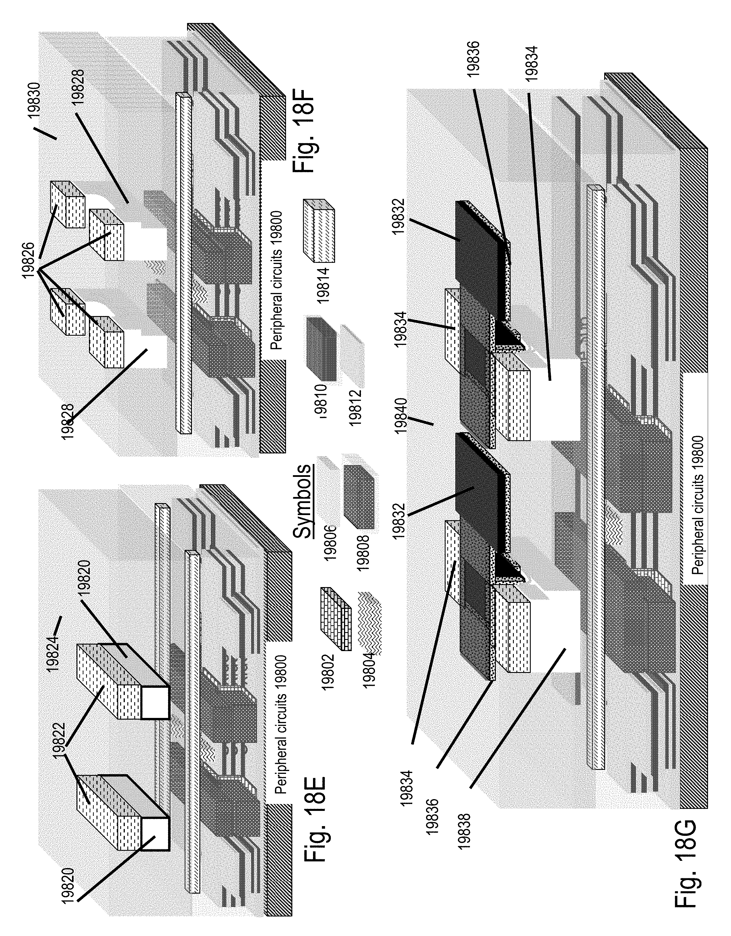
D00014
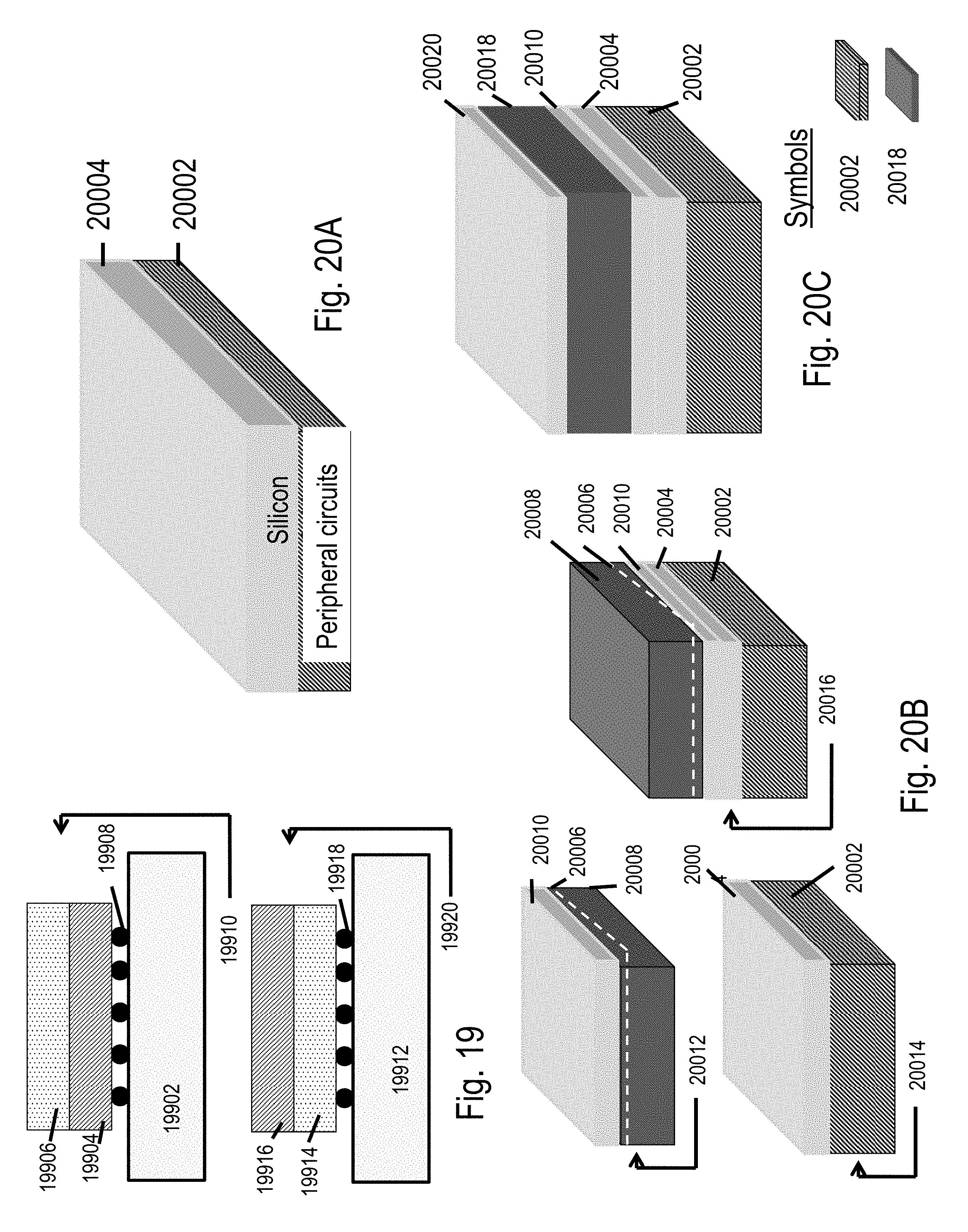
D00015
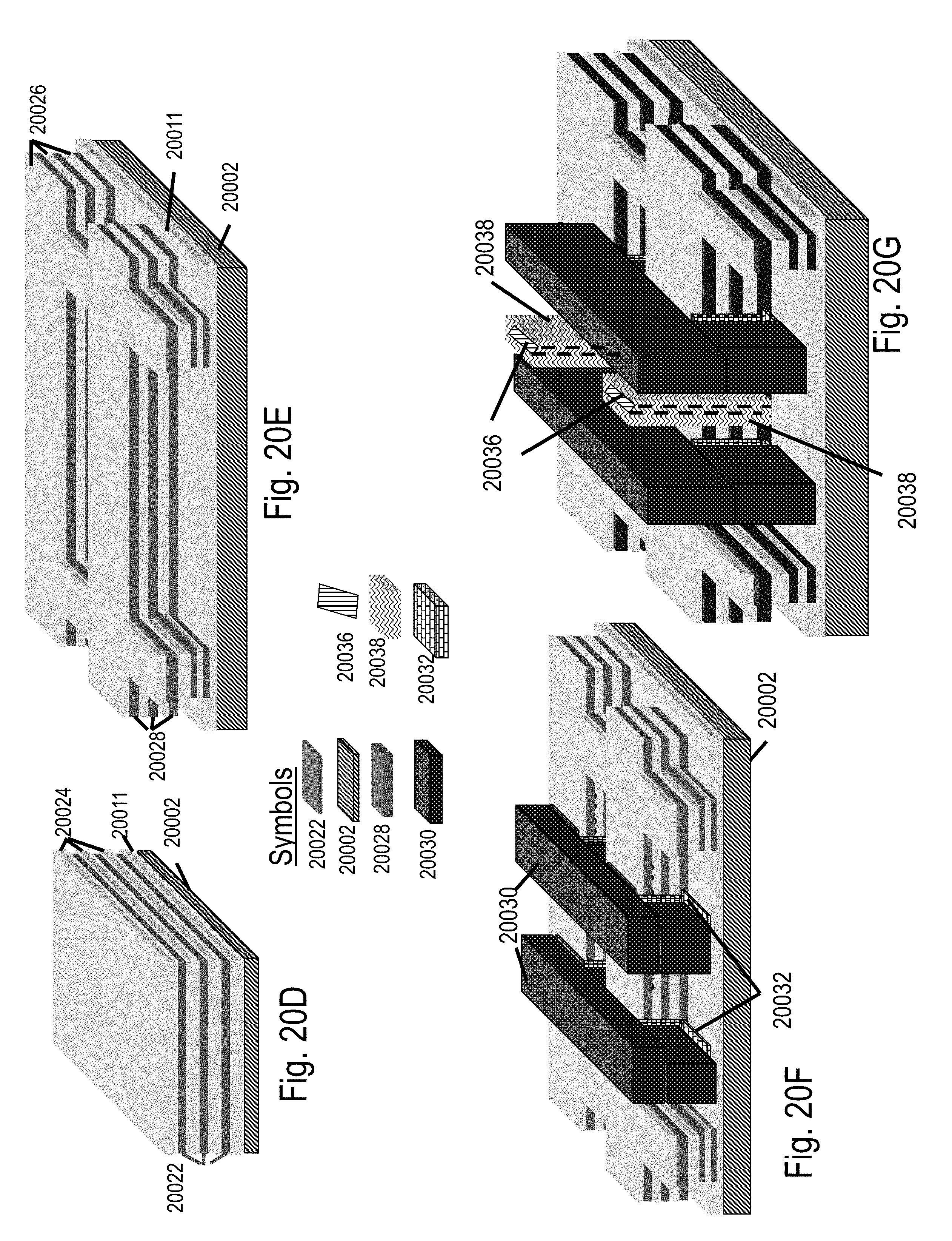
D00016

D00017

D00018
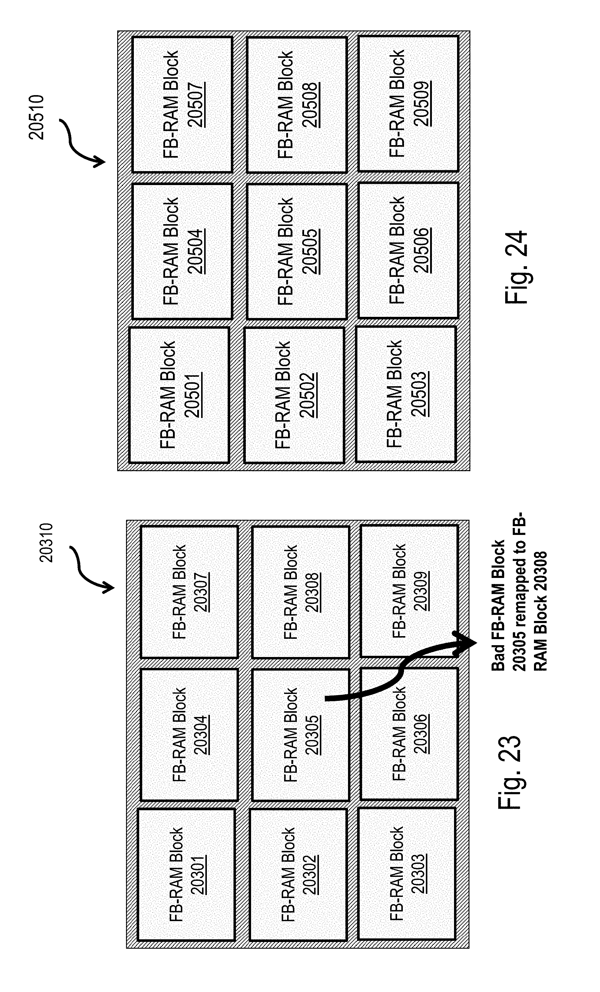
D00019

D00020

D00021
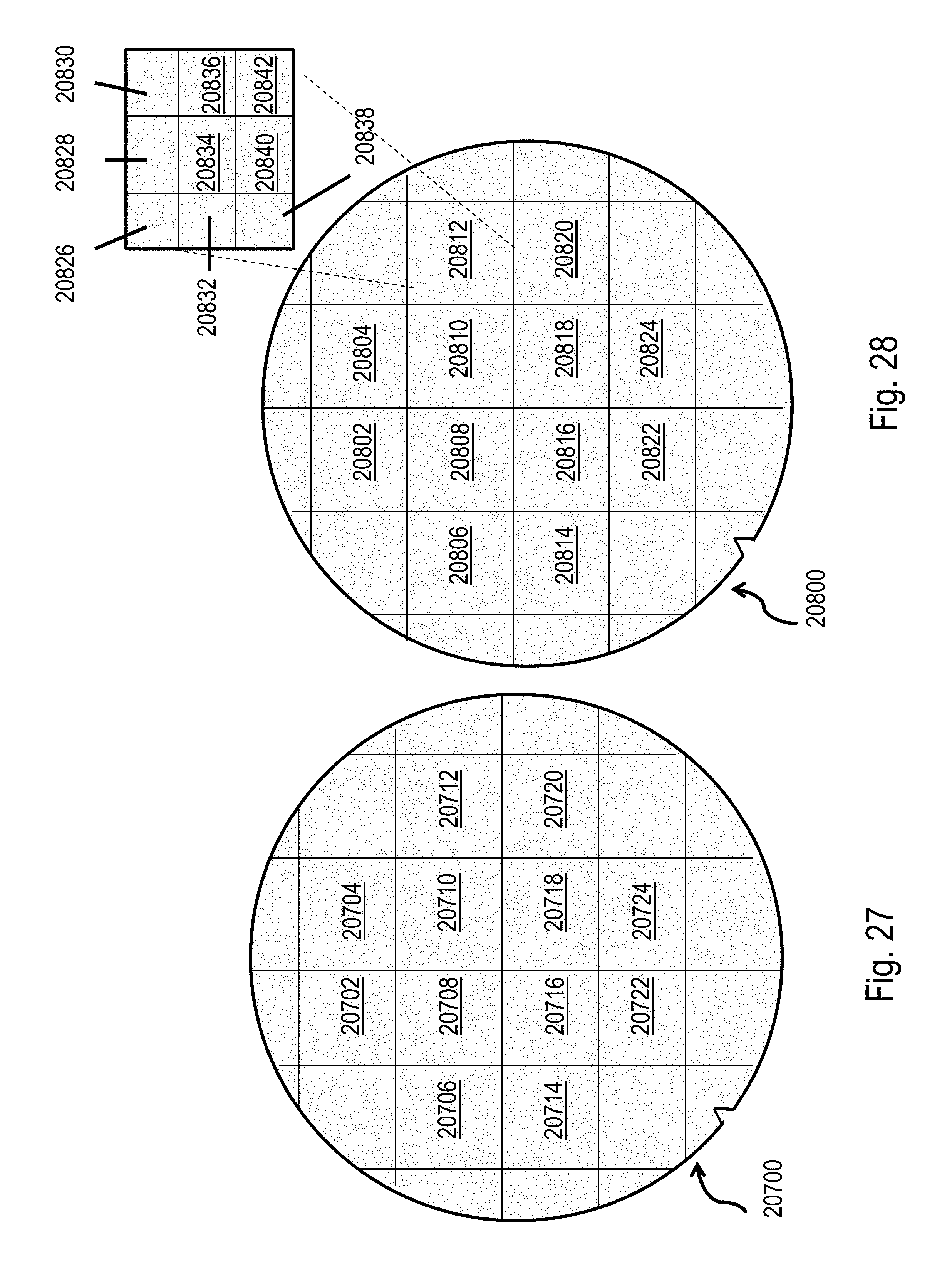
D00022

D00023

D00024

D00025
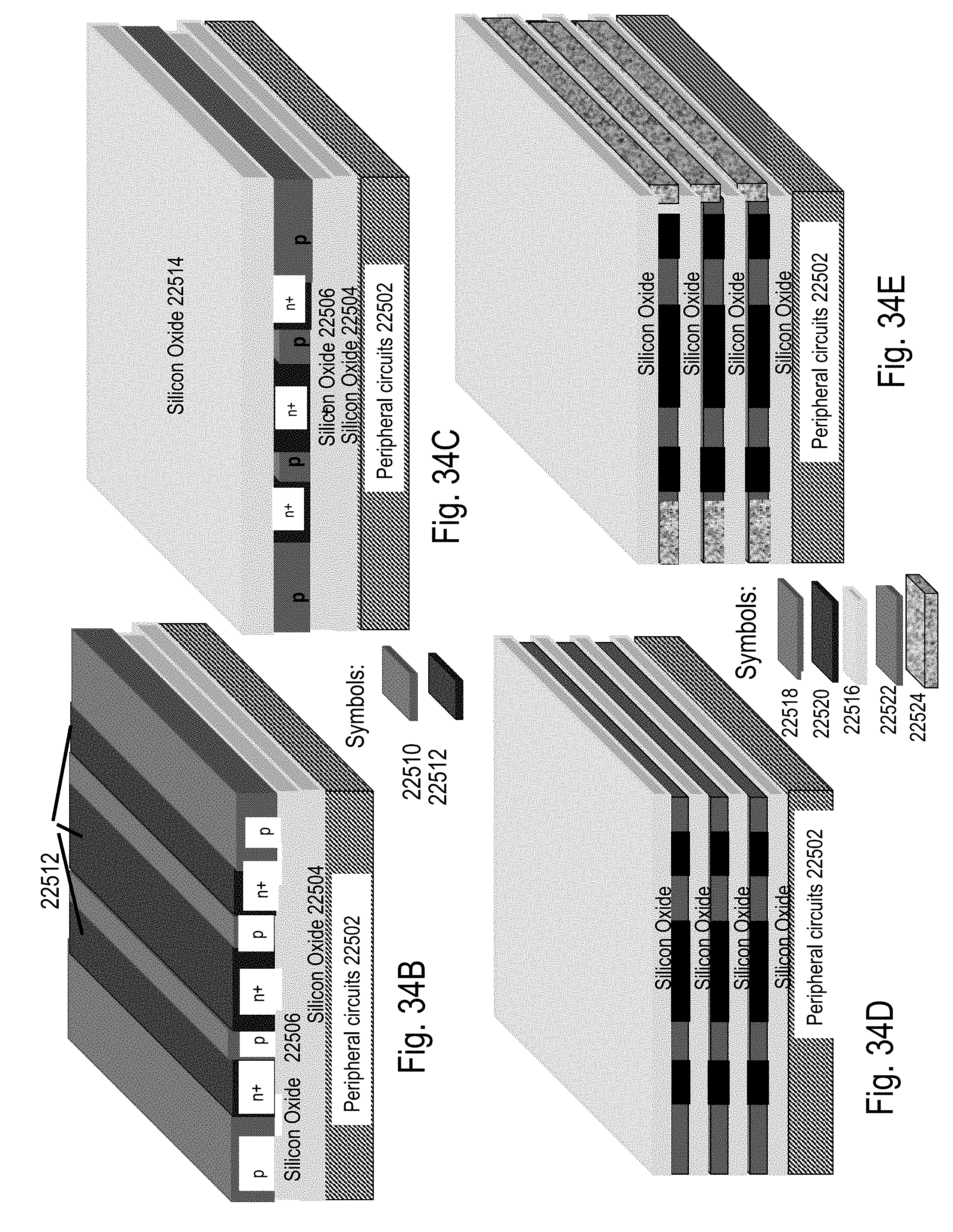
D00026

D00027
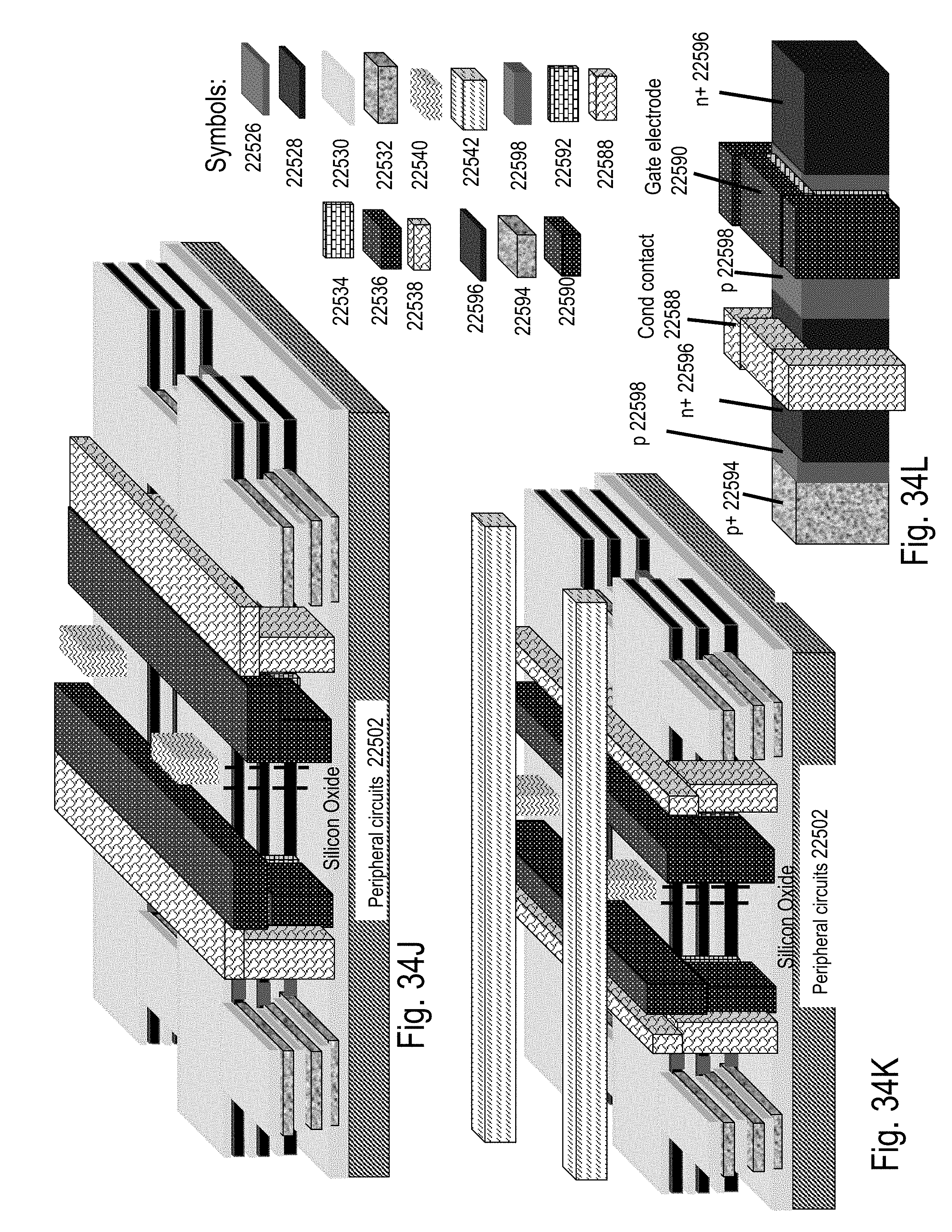
D00028
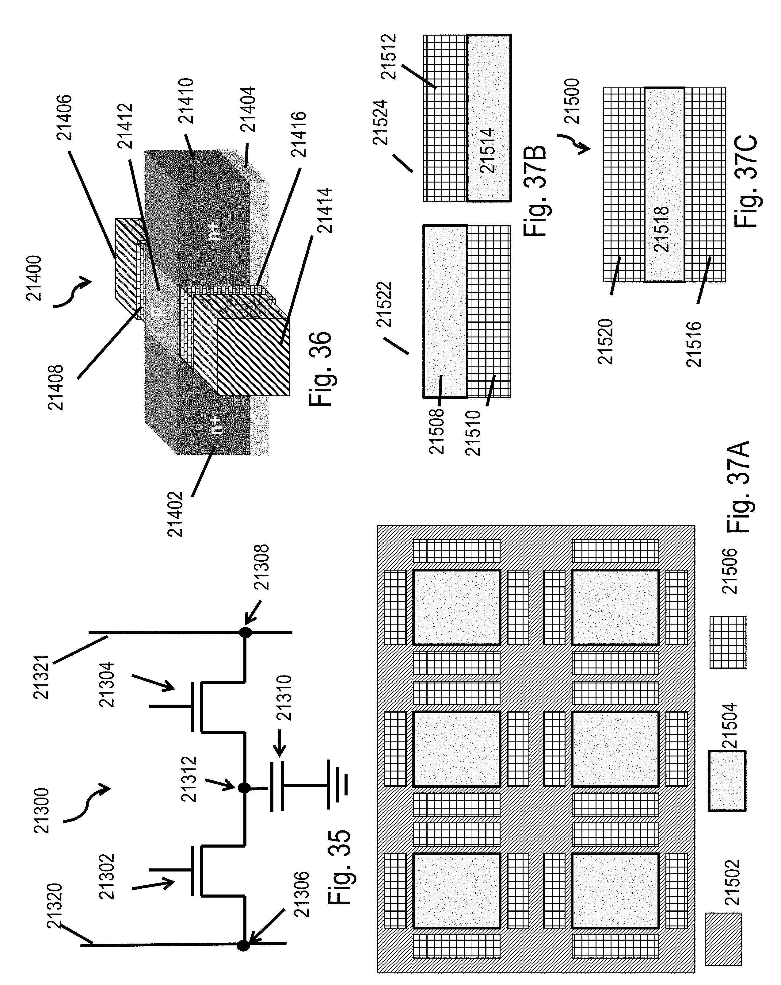
D00029

D00030

D00031

D00032

D00033

D00034

D00035
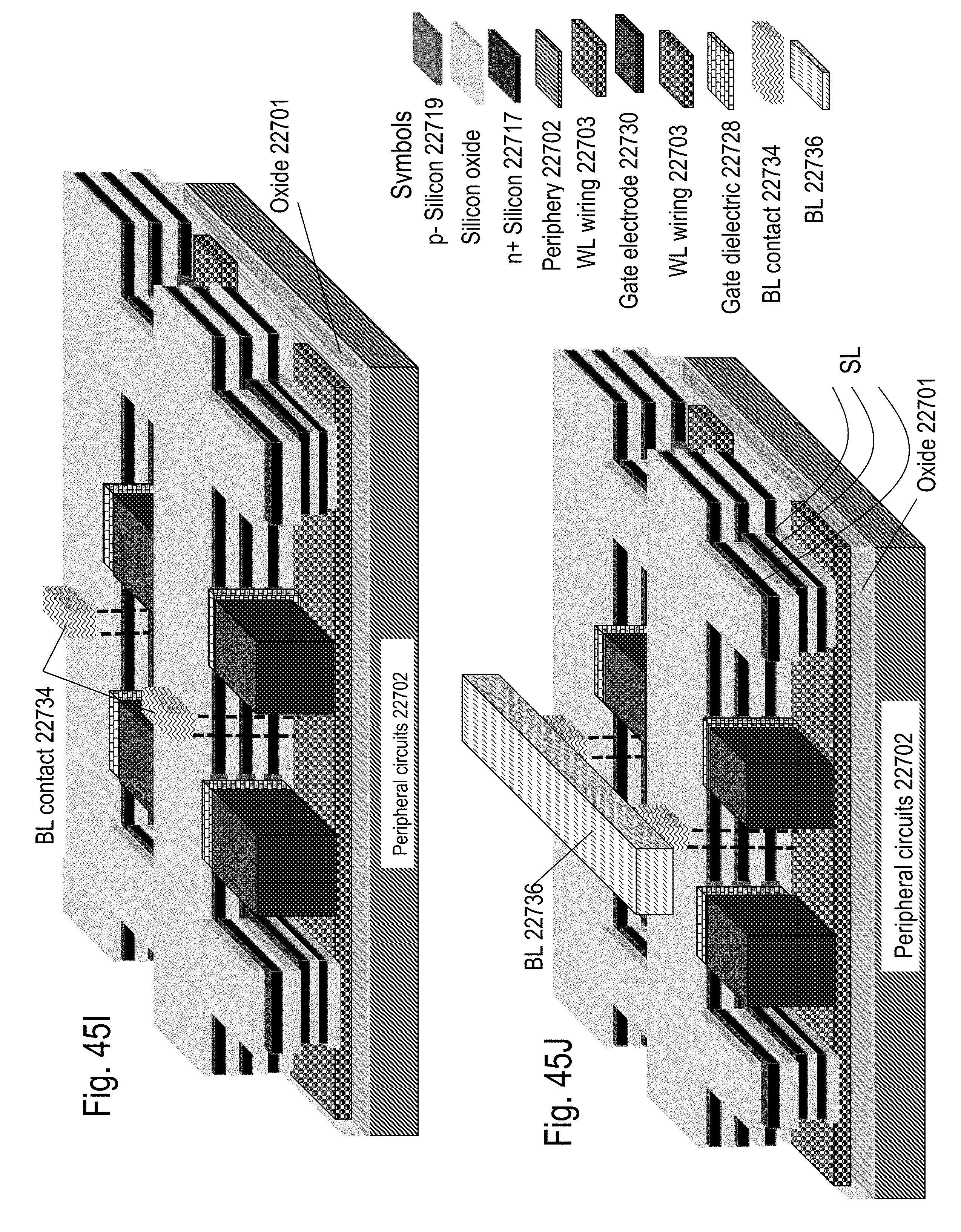
D00036

D00037
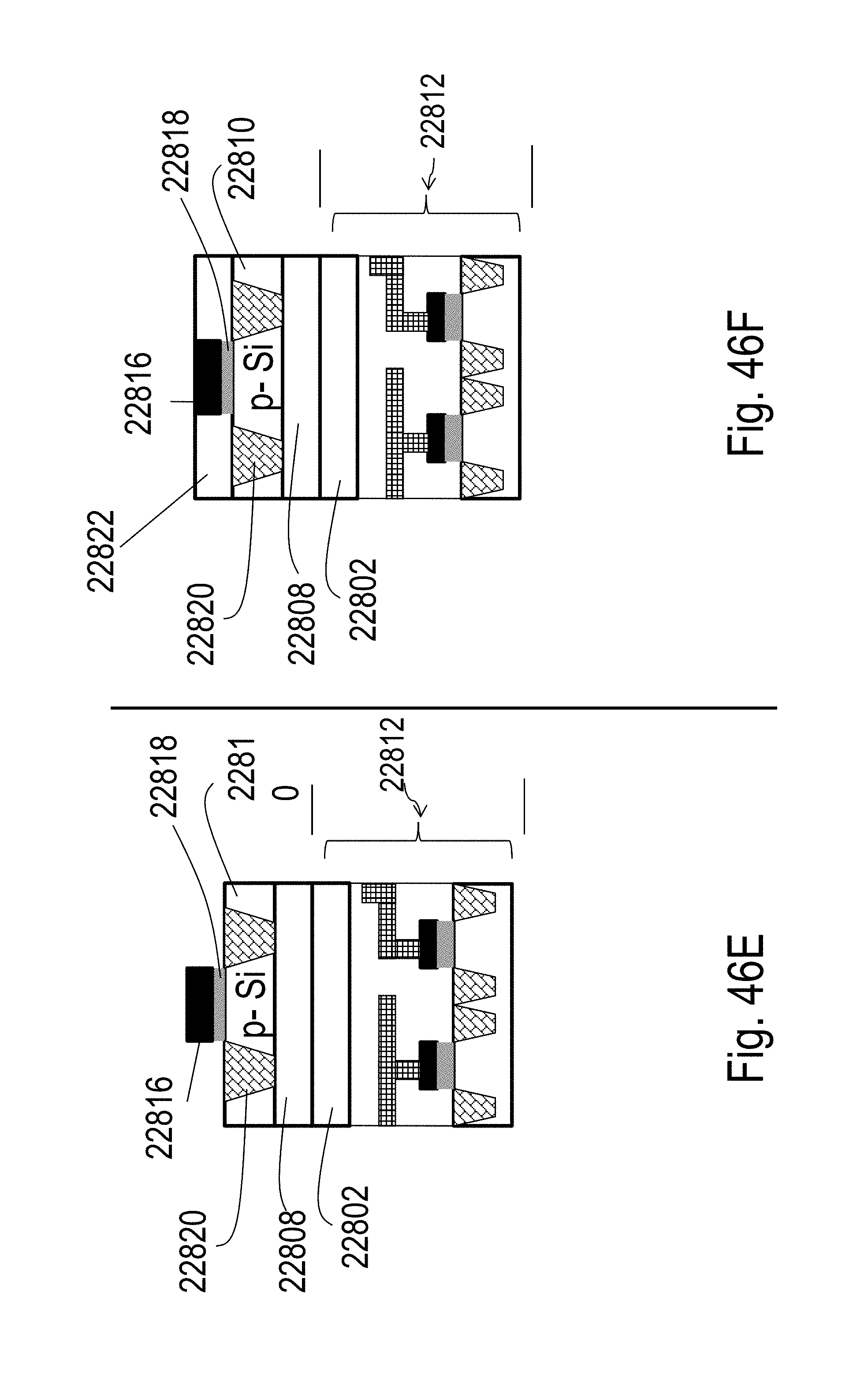
D00038
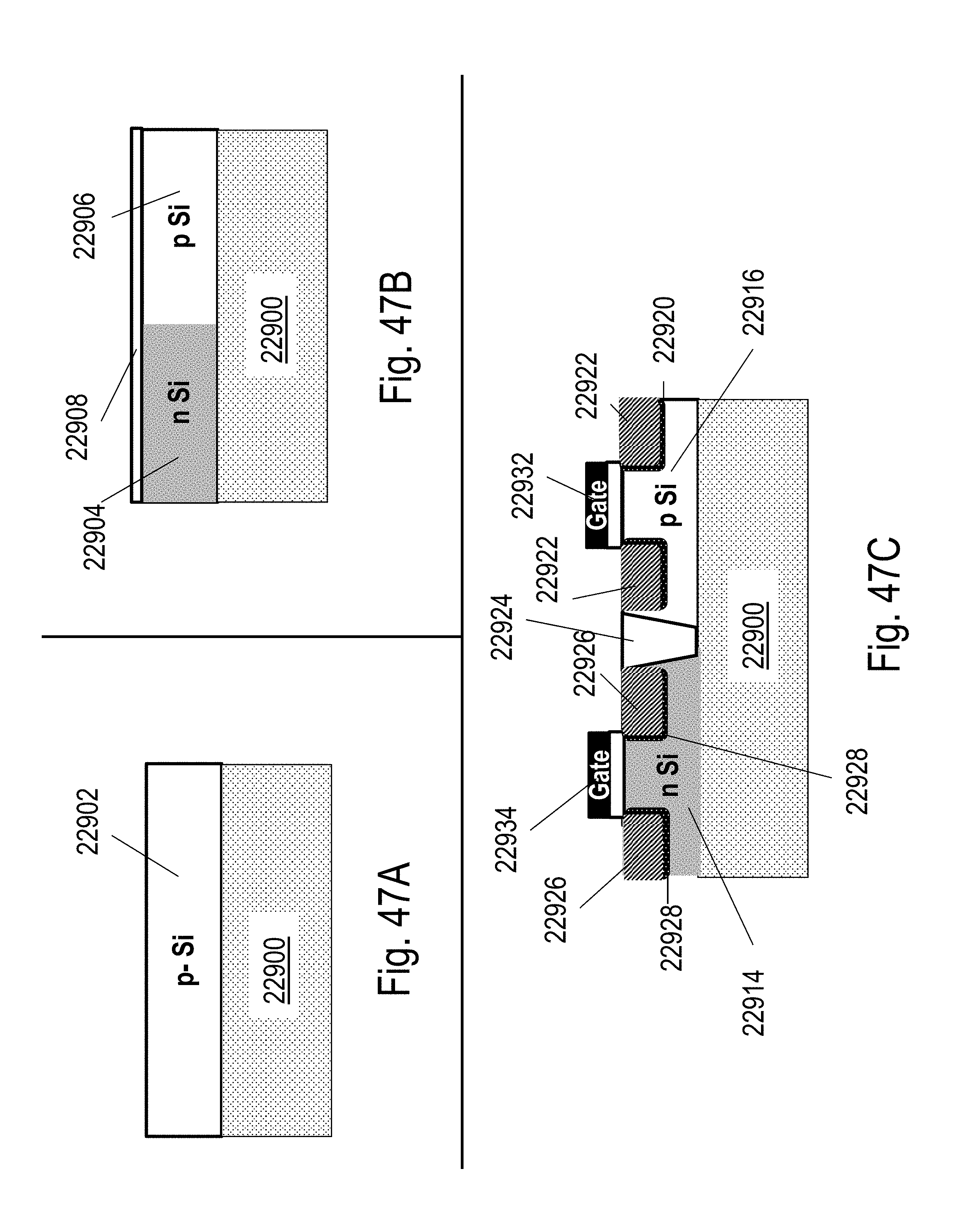
XML
uspto.report is an independent third-party trademark research tool that is not affiliated, endorsed, or sponsored by the United States Patent and Trademark Office (USPTO) or any other governmental organization. The information provided by uspto.report is based on publicly available data at the time of writing and is intended for informational purposes only.
While we strive to provide accurate and up-to-date information, we do not guarantee the accuracy, completeness, reliability, or suitability of the information displayed on this site. The use of this site is at your own risk. Any reliance you place on such information is therefore strictly at your own risk.
All official trademark data, including owner information, should be verified by visiting the official USPTO website at www.uspto.gov. This site is not intended to replace professional legal advice and should not be used as a substitute for consulting with a legal professional who is knowledgeable about trademark law.