Pixel Driver Circuit With Load-balance In Current Mirror Circuit
Nathan; Arokia ; et al.
U.S. patent application number 15/259978 was filed with the patent office on 2016-12-29 for pixel driver circuit with load-balance in current mirror circuit. The applicant listed for this patent is Ignis Innovation Inc.. Invention is credited to Shahin Jafarabadiashtiani, Arokia Nathan, Kapil V. Sakariya, Peyman Servati.
| Application Number | 20160379565 15/259978 |
| Document ID | / |
| Family ID | 34318786 |
| Filed Date | 2016-12-29 |


View All Diagrams
| United States Patent Application | 20160379565 |
| Kind Code | A1 |
| Nathan; Arokia ; et al. | December 29, 2016 |
PIXEL DRIVER CIRCUIT WITH LOAD-BALANCE IN CURRENT MIRROR CIRCUIT
Abstract
A pixel circuit for use in a display comprising a plurality of pixels is provided. The load-balanced current mirror pixel circuit can compensate for device degradation and/or mismatch, and changing environmental factors like temperature and mechanical strain. The pixel circuit comprises a pixel drive circuit comprising, switching circuitry, a current mirror having a reference transistor and a drive transistor, the reference transistor and the drive transistor each having a first and second node and a gate, the gate of the reference transistor being connected to the gate of the drive transistor; and a capacitor connected between the gate of the reference transistor and a ground potential, and a load connected between the current mirror and a ground potential, the load having a first load element and a second load element, the first load element being connected to the first node of the reference transistor and the second load element being connected to the first node of the drive transistor.
| Inventors: | Nathan; Arokia; (Cambridge, GB) ; Sakariya; Kapil V.; (Sunnyvale, CA) ; Servati; Peyman; (Vancouver, CA) ; Jafarabadiashtiani; Shahin; (Waterloo, CA) | ||||||||||
| Applicant: |
|
||||||||||
|---|---|---|---|---|---|---|---|---|---|---|---|
| Family ID: | 34318786 | ||||||||||
| Appl. No.: | 15/259978 | ||||||||||
| Filed: | September 8, 2016 |
Related U.S. Patent Documents
| Application Number | Filing Date | Patent Number | ||
|---|---|---|---|---|
| 13933554 | Jul 2, 2013 | 9472138 | ||
| 15259978 | ||||
| 10554795 | Jun 15, 2006 | 8502751 | ||
| PCT/CA2004/001741 | Sep 23, 2004 | |||
| 13933554 | ||||
| Current U.S. Class: | 345/690 |
| Current CPC Class: | G09G 3/325 20130101; G09G 3/3266 20130101; G09G 2300/0417 20130101; G09G 2320/0646 20130101; G09G 2300/0809 20130101; H05B 45/60 20200101; G09G 3/3283 20130101; G09G 2300/0842 20130101; G09G 3/3241 20130101; H05B 47/10 20200101; G09G 2300/0819 20130101 |
| International Class: | G09G 3/3241 20060101 G09G003/3241; H05B 33/08 20060101 H05B033/08; G09G 3/325 20060101 G09G003/325; G09G 3/3266 20060101 G09G003/3266; G09G 3/3283 20060101 G09G003/3283 |
Foreign Application Data
| Date | Code | Application Number |
|---|---|---|
| Sep 23, 2003 | CA | 2443206 |
Claims
1-27. (canceled)
28. A pixel driver circuit for use in a display, comprising: a light emitting device (LED) comprising a first terminal connected to a source of a first potential and at least one second terminal; a current mirror configured to provide a drive current to the LED based on a reference current; and, a switching circuit configured to convey the reference current to the current mirror; wherein the current mirror comprises: a reference transistor comprising a source terminal, a gate terminal connected to the switching circuit, and a drain terminal connected to the switching circuit, a drive transistor comprising a gate terminal connected to the gate terminal of the reference transistor, a source terminal, and a drain terminal, the drive transistor configured to convey the drive current to the LED; wherein one of the drain terminal and the source terminal of the reference transistor and a corresponding one of the drain terminal and the source terminal of the drain transistor are connected to the at least one second terminal of the LED; and a capacitor connected to the gate terminal of the reference transistor for accumulating a program voltage while the reference current is conveyed to the reference transistor.
29. The pixel driver circuit of claim 28, wherein the switching circuit comprises: a switch transistor comprising a gate terminal connected to a first select line, a first terminal connected to a data line, and a second terminal; and a feedback transistor comprising a gate terminal connected to the first select line or a second select line, a first terminal connected to one of the first terminal or the second terminal of the switch transistor, and a second terminal; wherein one of the second terminal of the switch transistor and the second terminal of the feedback transistor is connected to the gate terminal of the reference transistor, and the other of the second terminals of the switch transistor and the feedback transistor is connected to the drain terminal of the reference transistor.
30. The pixel driver circuit of claim 28, wherein the source terminal of the reference transistor and the source terminal of the drive transistor are connected to a common node, and wherein the at least one second terminal of the LED is connected to said common node.
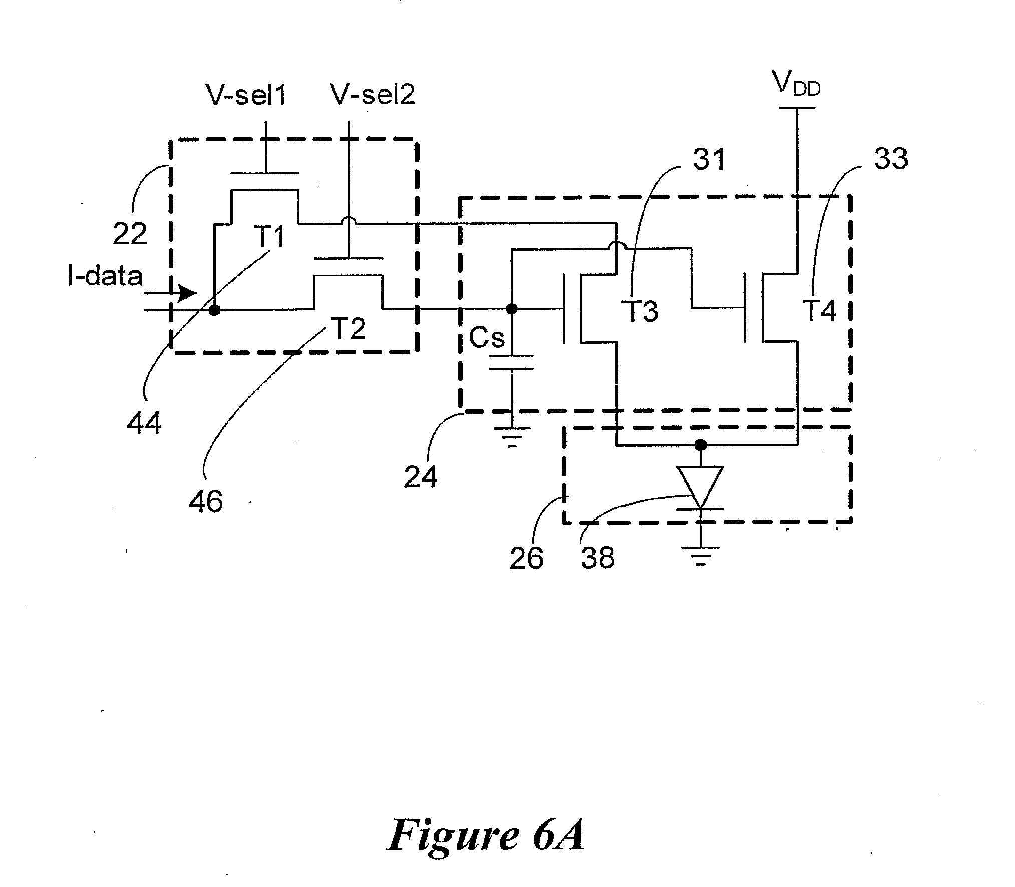
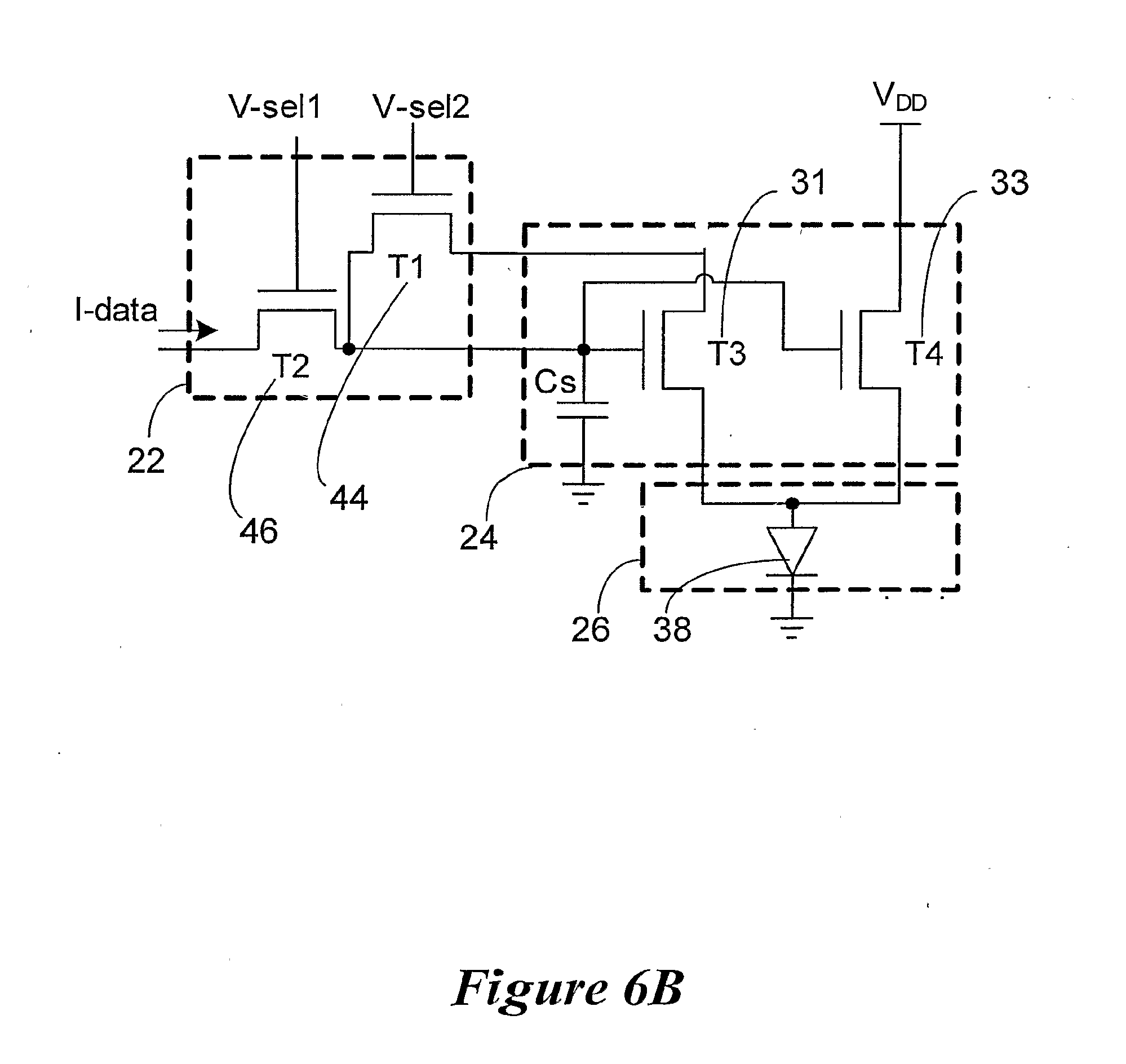
31. The pixel driver circuit of claim 28, wherein the at least one second terminal of the LED comprises two LED terminals connected to the source terminal of the reference transistor and the source terminal of the drive transistor, respectively.
32. The pixel driver circuit of claim 31, wherein the LED comprises a light emitting diode having a bottom electrode partitioned to form the two LED terminals.
33. The pixel driver circuit of claim 31, wherein the LED comprises a first light emitting diode connected between the source terminal of the reference transistor and the source of the first potential, and a second light emitting diode connected between the source terminal of the drive transistor and the source of the first potential.
34. The pixel driver circuit of claim 28, wherein the at least one second terminal of the LED comprises two LED terminals connected to the drain terminal of the reference transistor and the drain terminal of the drive transistor, respectively.
35. The pixel driver circuit of claim 31, wherein the LED comprises a light emitting diode having a bottom electrode partitioned to form the two LED terminals.
36. The pixel driver circuit of claim 34, wherein the LED comprises a first light emitting diode connected between the drain terminal of the reference transistor and the source of the first potential, and a second light emitting diode connected between the drain terminal of the drive transistors and the source of the first potential.
37. The pixel driver circuit of claim 34, wherein the LED comprises a first light emitting diode connected between the drain terminal of the reference transistor and a source of a second potential, and a second light emitting diode connected between the drain terminal of the drive transistors and the source of the first potential.
38. The pixel driving circuit of claim 34, wherein the first potential is a biasing potential that is sufficient to operate the drive transistor in a saturation regime.
39. The pixel driving circuit of claim 38, wherein the source terminal of the drive transistor and the source terminal of the reference transistor are connected to a source of a ground potential.
40. The pixel driving circuit of claim 30, wherein the first potential is a ground potential and wherein the drain terminal of the drive transistor is connected to a source of supply voltage that is sufficient to operate the drive transistor in a saturation regime.
41. The pixel driving circuit of claim 31, wherein the first potential is a ground potential and wherein the drain terminal of the drive transistor is connected to a source of supply voltage that is sufficient to operate the drive transistor in a saturation regime.
42. The pixel driver circuit according to claim 28, wherein the reference and drive transistors are thin film transistors.
43. The pixel driver circuit according to claim 42, wherein the thin film transistors are formed using amorphous silicon or polycrystalline silicon or an organic material.
44. The pixel driver circuit according to claim 42, wherein the reference and drive transistors are p-type.
45. The pixel driver circuit according to claim 42, wherein the reference and drive transistors are n-type.
46. The pixel driver circuit according to claim 28, incorporated in an active matrix organic light emitting display (AMOLED).
Description
FIELD OF INVENTION
[0001] The present invention relates to circuitry for use in an active matrix display, and more particularly to a current drive circuitry used to drive the electro-luminescent elements.
BACKGROUND OF THE INVENTION
[0002] OLED based displays have gained significant interest recently for many display applications because of their faster response times, larger viewing angles, higher contrast, lighter weight, lower power, and amenability to flexible substrates, as compared to liquid crystal displays (LCDs).
[0003] The simplest way of addressing an OLED display is to use a passive matrix format. Although passive matrix addressed OLED displays are already in the marketplace, they do not support the resolution needed for next generation displays, which use high information content (HIC) formats. HIC formats are only possible with an active matrix addressing scheme.
[0004] Active matrix addressing involves a layer of backplane electronics, based on thin-film transistors (TFTs). These thin film transistors provide the bias voltage and drive current needed in each OLED pixel and may be fabricated using amorphous silicon (a-Si:H), polycrystalline silicon (poly-Si), organic, polymer, or other transistor technologies. When compared to passive matrix addressing, active matrix addressing uses a lower voltage on each pixel and the current throughout the entire frame period is a low constant value. Thus, active matrix addressing avoids the excessive peak driving and leakage currents associated with passive matrix addressing. This increases the lifetime of the OLED.
[0005] LCDs are electric field driven devices. OLEDs, on the other hand, are current driven devices. Thus, the brightness and stability of the light emitted by a given OLED used in a display is dependent on the operation of the TFTs in the current drive circuit. Thus AMOLED displays are far more sensitive to TFT instabilities including, spatial and temporal variations in transistor threshold voltage, mobility instability, and mismatch issues. These instabilities need to be addressed for widespread use of OLED based displays.
[0006] FIG. 1 presents a graph of threshold voltage shift vs. stress voltage for various times for amorphous silicon based TFTs. It is readily apparent from FIG. 1 that the threshold voltage of the transistors varies over time. If these transistors were used in a display, the variation in threshold voltage would likely result in variation in the brightness of the OLED across the array and/or a decrease in brightness over time, both of which are unacceptable.
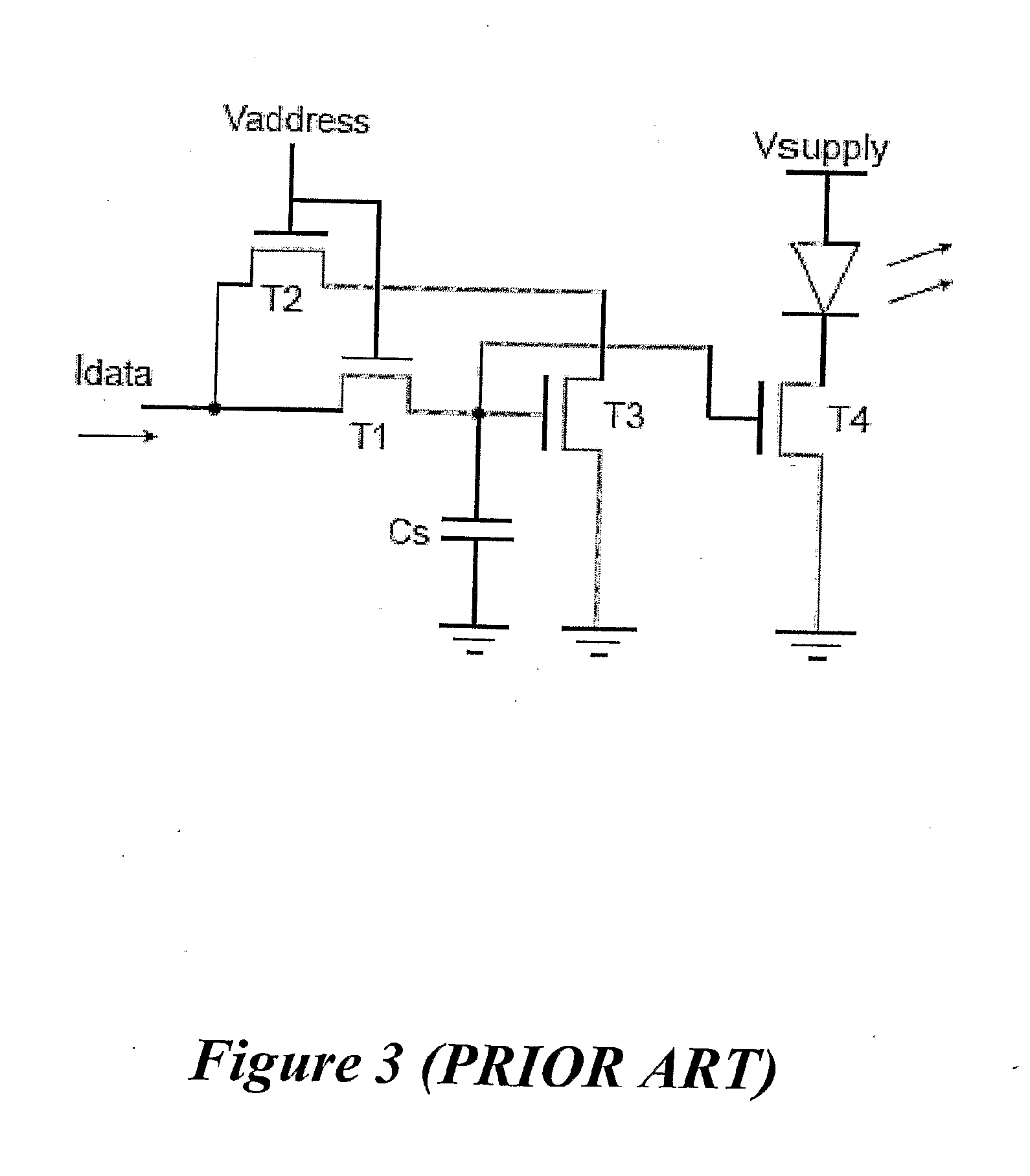
[0007] A simple pixel driver circuit is shown in FIG. 2. This "2T" circuit is a voltage programmed circuit. Such a circuit is not practical for OLED displays as such a circuit can not compensate for variations in transistor threshold voltage. One solution to this variation in threshold voltage is to use a current programmed circuit to drive the OLED of the pixels. Current programming is a good method for driving AMOLED displays since the OLED is a current driven device, and its brightness is approximately linearly dependent upon the current flowing through it.
[0008] One such current programmed circuit is presented in FIG. 3. This circuit incorporates a current-mirror which compensates for any shift or mismatch in the threshold voltage of the drive transistor 12 which ensures that the brightness of the OLED 14 does not decrease over time. This feature of the circuit allows its drive characteristics to be much improved as compared to the 2T circuit of FIG. 2.
[0009] When programming the circuit of FIG. 3, V.sub.ADDRESS is high and a current I.sub.DATA is applied. This current initially flows through transistor T1 and charges capacitor C.sub.S. As the capacitor voltage rises, T3 begins to turn on and (.sub.DATA starts to flow through T2 and T3 to ground. The capacitor voltage stabilizes at the point when all of I.sub.DATA flows through T2 and T3, and none through T1. This process is independent of the threshold voltage V.sub.T of transistors T3 and T4.
[0010] The gates of T3 and T4 are connected, so the current flowing through T3 is mirrored in T4. This topology allows us to have on-pixel current gain or attenuation depending on the sizing of T3 and T4, so that the respective data current can be proportionately smaller or larger than the OLED current. In an active matrix array, pixels are scanned and programmed in a row-by-row fashion. The time taken to scan all rows (one frame) is called the frame time. During array operation, the switching TFTs (T1 and T2) are ON only once in the frame time.
[0011] However, existing current programmed circuits do not adequately address long-term stability in the OLED drive current due to differential Vt-shift and other bias, temperature, or mechanical stress related degradations and mismatches in the current mirror.
SUMMARY OF THE INVENTION
[0012] The present invention relates to a circuit for driving light emitting elements in a display and more particularly relates to a current drive circuit that implements a current mirror wherein each transistor of the current mirror is connected to a load.
[0013] It is an object of the invention to provide improvedAMOLED Display Backplanes and Pixel Driver Circuits.
[0014] Accordingly, it is an object of the present invention to provide pixel current driver circuits for active matrix organic light emitting displays (AMOLED), capable of providing stable and predictable drive currents, in the presence of device degradation and/or mismatch, and changing environmental factors like temperature and mechanical strain. The latter is particularly important for mechanically flexible AMOLED displays.
[0015] According to an aspect of the invention a pixel circuit for use in a display comprising a plurality of pixels is provided. The pixel circuit comprises a pixel drive circuit comprising, switching circuitry, a current mirror having a reference transistor and a drive transistor, the reference transistor and the drive transistor each having a first and second node and a gate, the gate of the reference transistor being connected to the gate of the drive transistor; and a capacitor connected between the gate of the reference transistor and a ground potential, and a load connected between the current mirror and a ground potential, the load having a first load element and a second load element, the first load element being connected to the first node of the reference transistor and the second load element being connected to the first node of the drive transistor.
[0016] According to another aspect of the invention a pixel circuit for use in a display comprising a plurality of pixels is provided. The pixel circuit comprises a pixel drive circuit comprising, switching circuitry, a current mirror having a reference transistor and a drive transistor, the reference transistor and the drive transistor each having a first and second node and a gate, the gate of the reference transistor being connected to the gate of the drive transistor, the second node of the reference and drive transistors connected to a ground potential, and a capacitor connected between the gate of the reference transistor and a ground potential, and a load connected between the current mirror and a potential.
[0017] This summary of the invention does not necessarily describe all features of the invention.
BRIEF DESCRIPTION OF THE DRAWINGS
[0018] These and other features of the invention will become more apparent from the following description in which reference is made to the appended drawings wherein:
[0019] FIG. 1 shows a graph of threshold voltage shift v. gate stress voltage for various times for thin film transistors made from amorphous silicon;
[0020] FIG. 2 shows a schematic diagram of a 2T voltage-programmed pixel driver circuit;
[0021] FIG. 3 shows a schematic diagram of a 4T current-programmed driver circuit;
[0022] FIG. 4 shows a block diagram of a current-programmed driver circuit according to an embodiment of the invention;
[0023] FIG. 5A shows a schematic diagram of a current-programmed driver circuit according to an embodiment of the invention;
[0024] FIG. 5B shows a schematic diagram of a current-programmed driver circuit according to an embodiment of the invention;
[0025] FIG. 5C shows a schematic diagram of a current-programmed driver circuit according to an embodiment of the invention;
[0026] FIG. 6A shows a schematic diagram of a current-programmed driver circuit according to an embodiment of the invention;
[0027] FIG. 6B shows a schematic diagram of a current-programmed driver circuit according to an embodiment of the invention;
[0028] FIG. 6C shows a schematic diagram of a current-programmed driver circuit according to an embodiment of the invention;
[0029] FIG. 7A shows a block diagram of a current-programmed driver circuit according to an embodiment of the invention;
[0030] FIG. 7B shows a schematic diagram of a current-programmed driver circuit according to an embodiment of the invention;
[0031] FIG. 7C shows a schematic diagram of a current-programmed driver circuit according to an embodiment of the invention;
[0032] FIG. 7D shows a schematic diagram of a current-programmed driver circuit according to an embodiment of the invention; and
[0033] FIG. 7E shows a schematic diagram of a current-programmed driver circuit according to an embodiment of the invention.
[0034] The above objects and features of the present invention will become more apparent by the following description of the preferred embodiments with reference to the attached drawings.
DETAILED DESCRIPTION
[0035] It has been found that the long-term stability of the OLED drive current can be addressed by providing a load to each transistor of the current mirror of a current based drive circuit.
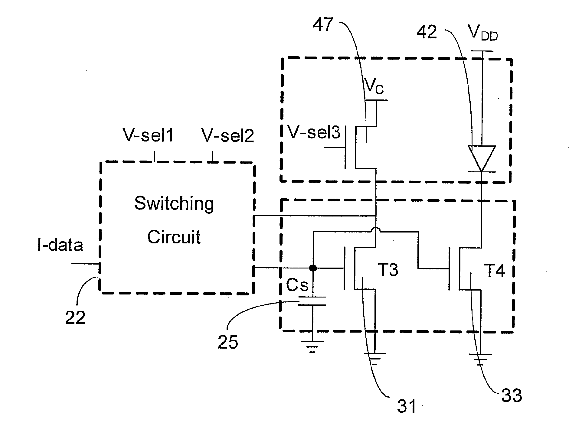
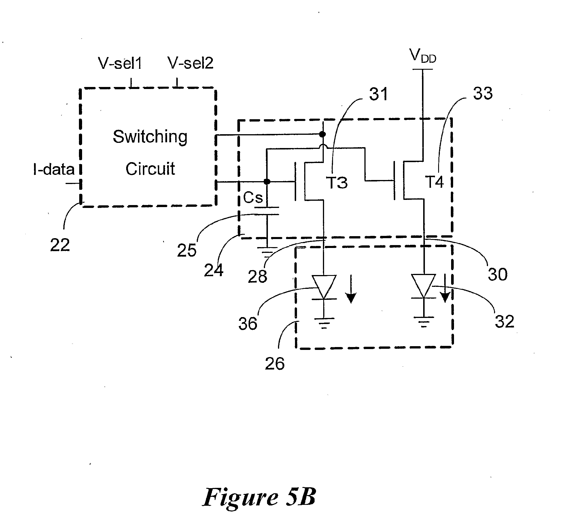
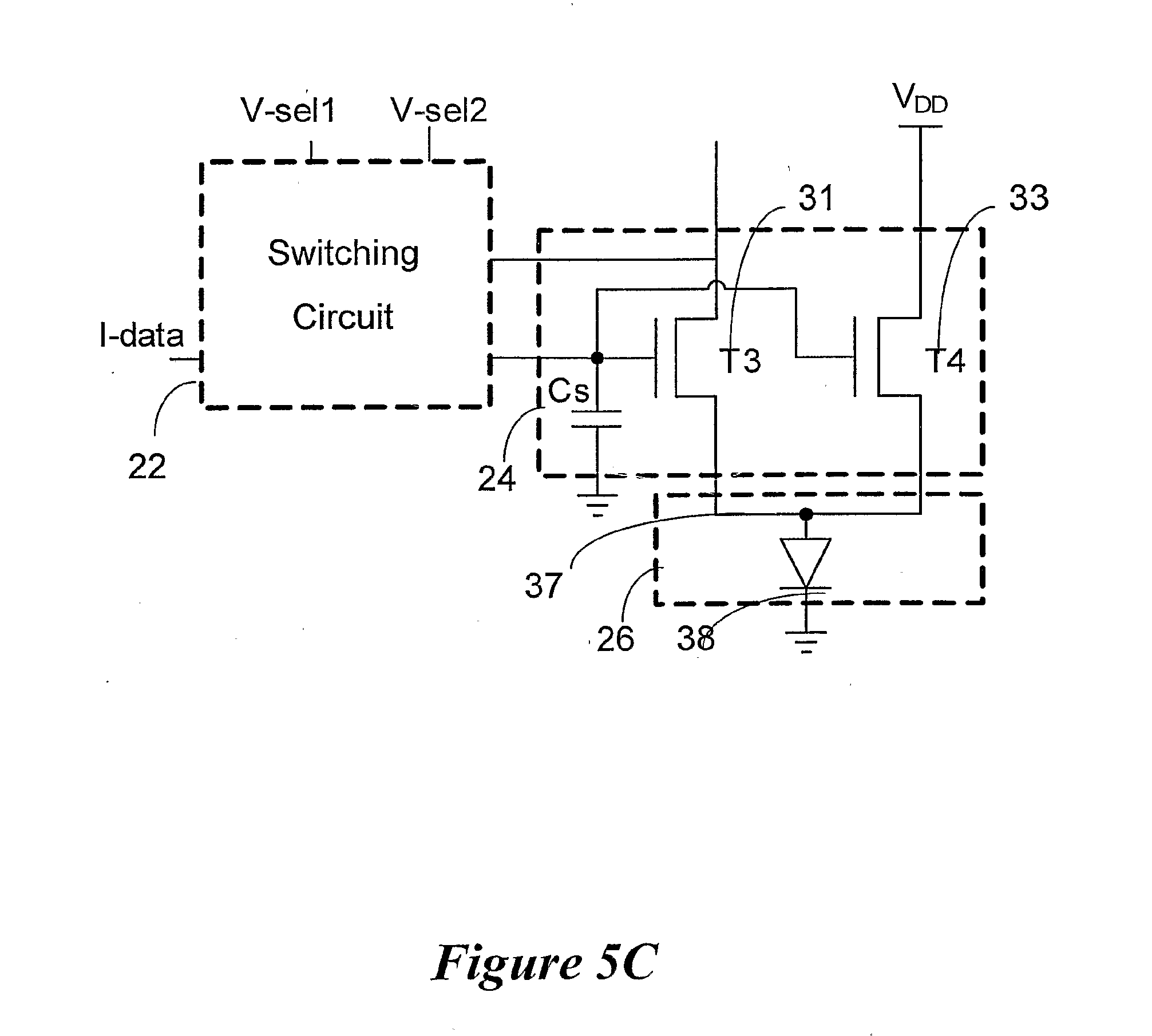
[0036] A block diagram of a pixel driver circuit according to one aspect of the invention is shown in FIG. 4. The driver circuit can generally be considered to include a switching circuit 22, a current mirror 24 and a load 26. Of particular note is that the load 26 is configured, with respect to the current mirror 24, such that the two transistors of the current mirror 24 have a load connected to them. In the configuration shown in FIG. 4 the load 26 is connected between the current mirror 24 and ground with connections 28 and 30. Where the connections 28 and 30 are each connected to a node of a transistor of the current mirror and the load 26. This architecture provides for a balancing of the load between the transistors of the current mirror. Embodiments of the invention that implement this architecture will now be presented.
[0037] In the embodiment presented in FIG. 4 the switching circuit 22 is connected to two select lines, namely V-sel1 and V-sel2. The embodiments presented in FIGS. 5A-5C, 6A-6C and 7A-7E likewise have two select lines. The switching circuit 22 is further connected to a single data line, I-data.
[0038] The circuits presented in FIGS. 5A to 5C have the same basic architecture as the circuit presented in FIG. 4, i.e. both transistors of the current mirror are connected to the load 26. The circuits of FIGS. 5A to 5C present type and configuration variations for the load 26.
[0039] In FIG. 5A the current mirror 24 includes a reference transistor 31, a drive transistor 33. The transistors 31 and 33 are thin film transistors which have an amorphous silicon channel. A storage capacitor 25 is included in the current mirror 24. The gates of the transistor 31 and the transistor 33 are tied together and both connected to a plate of the storage capacitor 25. The other plate of the storage capacitor Cs is connected to ground. The source of the reference transistor 31 is connected to potential Vc and the drain is connected to the switching circuit 22. Connecting the source to the potential Vc allows the two sides of the current mirror to be balanced with proper biasing. The source of the drive transistor 33 is connected to a light emitting diode 32 and the drain is connected to V.sub.DD. In this embodiment the light emitting diode 32 is an organic light emitting diode (OLED).
[0040] FIG. 5B is a schematic diagram of a pixel driver circuit according to another embodiment of the invention. In this embodiment the source of the reference transistor 31 and the drive transistor 33 are connected to light emitting diodes 36 and 32, respectively.
[0041] FIG. 5C presents the currently preferred configuration for the load 26. The transistors 31 and 33 are tied together using a connection 37. In FIG. 5C the connection 37 is pictorially located within the load 26. The current embodiment is not limited by this representation. A single OLED 37 is connected to the common connection 37.
[0042] FIGS. 6A to 6C present embodiments of the invention wherein the current mirror 24 and the load 26 are the same as the embodiment presented in FIG. 5C while various configurations of the switching circuitry are provided. The switching circuits presented in FIGS. 6A to 6C each have a feedback transistor 44 and a switch transistor 46.
[0043] In the circuit presented in FIG. 6A one terminal of the feedback transistor 44 and one terminal of the switch transistor 46 are connected to data line I-data. The second terminal of the feedback transistor 44 is connected to the drain of reference transistor 31 while the second terminal of the switch transistor 46 is connected to the gate of the reference and drive transistors 31 and 33, respectively. Finally, the gate of the feedback transistor 44 and switch transistor 46 is connected to the select line V-sel1 and select line V-sel2, respectively.
[0044] In the embodiment presented in FIG. 6B the first terminal of the switch transistor 46 is connected to the data line I-data while the first terminal of the feedback transistor 44 is connected to the second terminal of the switch transistor 46 which is connected to the gate of the reference and drive transistors 31 and 33, respectively. The second terminal of the feedback transistor 44 is connected to the drain of the reference transistor 31. Finally, the gate of the feedback transistor 44 and switch transistor 46 is connected to the select line V-sel2 and select line V-sel1, respectively.
[0045] In the embodiment presented in FIG. 6C the first terminal of the switch transistor 46 is connected to the data line I-data while the first terminal of the feedback transistor 44 is connected to the second terminal of the switch transistor 46 which is connected to the drain of the reference transistor 31. The second terminal of the feedback transistor 44 is connected to the gate of the reference and drive transistors 31 and 33, respectively. Finally, the gate of the switch transistor 46 and feedback transistor 44 is connected to the select line V-sel1 and select line V-sel2, respectively.
[0046] The circuits that have been considered are embodiments of the circuit presented as a block diagram in FIG. 4. An alternative embodiment of the circuit architecture of FIG. 4 is presented in FIG. 7A. The organization of the switching circuit 22 and the current mirror 24 is the same as the embodiment presented in FIG. 4. In this embodiment the load 26 is arranged such that it is between the potential V.sub.DD and the current mirror 24. FIG. 7B-7E present embodiments of the invention based on the block diagram of FIG. 7A. These embodiments implement the same circuit for the current mirror 24 while the configuration of the load 26 varies.
[0047] In the embodiment presented in FIG. 7B the load 26 includes light emitting diodes 40 and 42. The diodes 40 and 42 are connected between the potential V.sub.DD and the drain of reference transistor 31 and drive transistor 33, respectively. The sources of the reference transistor 31 and the drive transistor 33 are connected to ground. The gates of the reference transistor 31 and the drive transistor 33 are tied together and connected to both the switching circuit 22 and a plate of the storage capacitor 25. In the embodiment presented in FIG. 7C the light emitting diode 40 is connected to a potential V.sub.C and the diode 42 is connected to the potential V.sub.DD. The embodiments presented in FIGS. 7D and 7E differ from the embodiments of FIGS. 7B and 7C, respectively, in that the light emitting diode 40 is replaced with a transistor 47. The gate of transistor 47 is connected to a third select line V-sel3, a first terminal is connected to a potential and a second terminal is connect to the source terminal of reference transistor 32.
[0048] In the schematic diagram of FIGS. 5B, 7B, and 7C there are two OLEDs in each pixel. Such a double OLED structure is formed by partitioning the bottom electrode of the OLED of each pixel into two electrodes. Partitioning of the electrode provide for the formation of two OLEDs in each pixel. One of the OLEDs is connected to the drive transistor and the other is connected to the reference transistor. Therefore the load of reference and drive transistors is the same, resulting in a minimization of mismatches between these two transistors. It is noted that the ratio between the areas of the two OLEDs and the gain of the current mirror can be engineered to achieve desired circuit performance.
[0049] According to an alternative embodiment of the invention the transistors can be any appropriate material for the fabrication of thin film transistors including polycrystalline silicon, polymer and organic materials. In particular this embodiment considers appropriate changes for including p-type TFTs that are relevant to persons skilled in the art.
[0050] According to another alternative embodiment of the invention the pixel drive circuits do not include the capacitor Cs.
[0051] According to another alternative embodiment of the invention the switching circuit 22 is appropriate for the use with a single select line.
[0052] According to another alternative embodiment of the invention the transistors of the pixel driver circuits may have more than one gate. In particular the transistors may be dual gate transistors.
[0053] According to another alternative embodiment of the invention there is more than one driver circuit for a given pixel. In particular there may be three pixel driver circuits as would be appropriate for pixels in an RGB or colour display.
[0054] The present invention has been described with regard to one or more embodiments. However, it will be apparent to persons skilled in the art that a number of variations and modifications can be made without departing from the scope of the invention as defined in the claims.
* * * * *
D00000
D00001
D00002
D00003
D00004
D00005
D00006
D00007
D00008
D00009
D00010
D00011
D00012

D00013

D00014

D00015

XML
uspto.report is an independent third-party trademark research tool that is not affiliated, endorsed, or sponsored by the United States Patent and Trademark Office (USPTO) or any other governmental organization. The information provided by uspto.report is based on publicly available data at the time of writing and is intended for informational purposes only.
While we strive to provide accurate and up-to-date information, we do not guarantee the accuracy, completeness, reliability, or suitability of the information displayed on this site. The use of this site is at your own risk. Any reliance you place on such information is therefore strictly at your own risk.
All official trademark data, including owner information, should be verified by visiting the official USPTO website at www.uspto.gov. This site is not intended to replace professional legal advice and should not be used as a substitute for consulting with a legal professional who is knowledgeable about trademark law.