Optical Pattern Projector
Thuries; Serge ; et al.
U.S. patent application number 14/747197 was filed with the patent office on 2016-12-29 for optical pattern projector. The applicant listed for this patent is Hand Held Products, Inc.. Invention is credited to Alain Gillet, Bernard Puybras, Serge Thuries.
| Application Number | 20160377414 14/747197 |
| Document ID | / |
| Family ID | 56117545 |
| Filed Date | 2016-12-29 |

| United States Patent Application | 20160377414 |
| Kind Code | A1 |
| Thuries; Serge ; et al. | December 29, 2016 |
OPTICAL PATTERN PROJECTOR
Abstract
An optical pattern projector used for projecting a structured-light pattern onto an object for dimensioning is presented. The optical pattern projector utilizes a laser array, a lenslet array, a lens, and a diffractive optical element to create a repeated pattern of projected dots. The pattern repetition is based on the grid pattern of laser array. Each laser's collimated beam, when projected through the lens, impinges on the diffractive optical element from a slightly different direction. The diffractive optical element creates a sub-patterns that continue propagating along these different directions and combine on a target to produce a repeating optical pattern.
| Inventors: | Thuries; Serge; (Saint Jean, FR) ; Gillet; Alain; (Toulouse, FR) ; Puybras; Bernard; (Saint Pierre De Lages, FR) | ||||||||||
| Applicant: |
|
||||||||||
|---|---|---|---|---|---|---|---|---|---|---|---|
| Family ID: | 56117545 | ||||||||||
| Appl. No.: | 14/747197 | ||||||||||
| Filed: | June 23, 2015 |
| Current U.S. Class: | 356/625 ; 359/558 |
| Current CPC Class: | G01B 11/02 20130101; G02B 27/0961 20130101; G02B 27/106 20130101; G02B 13/0005 20130101; G02B 27/0944 20130101; G02B 27/20 20130101; G02B 3/0056 20130101; H01S 5/423 20130101; G02B 27/4233 20130101; G01B 11/25 20130101; G02B 27/1093 20130101 |
| International Class: | G01B 11/25 20060101 G01B011/25; G02B 3/00 20060101 G02B003/00; G02B 13/00 20060101 G02B013/00; H01S 5/42 20060101 H01S005/42; G01B 11/02 20060101 G01B011/02; G02B 27/42 20060101 G02B027/42 |
Claims
1. An optical pattern projector, comprising: a laser array, having a plurality of lasers equally spaced in a grid pattern and configured to radiate light in the same direction; a lenslet array having a plurality of lenslets arranged so that each lenslet is aligned with a particular laser, the lenslet array positioned in front of the laser array to focus the radiated light from the lasers into a plurality of collimated laser beams; a lens positioned in front of the lenslet array and sufficiently large to receive all of the laser beams, the lens redirecting each laser beam along a particular incident angle determined by the spatial position of the particular laser beam in the grid pattern; and a diffractive optical element (DOE) positioned in front of the lens to receive all of the laser beams and, for each laser beam, to (i) create a sub-pattern and (ii) project each laser beam's sub-pattern towards a target along a particular angle determined by the particular laser beam's incident angle, wherein the sub-patterns from each laser beam combine on the target to form an optical pattern.
2. The optical pattern projector according to claim 1, wherein the laser array is an array of vertical cavity surface emitting lasers (VCSELs).
3. The optical pattern projector according to claim 2, wherein the laser array comprises more than 100 VCSELs.
4. The optical pattern projector according to claim 1, wherein the lens is an f-theta lens.
5. The optical pattern projector according to claim 1, wherein the sub-patterns from the laser beams are identical.
6. The optical pattern projector according to claim 1, wherein the optical pattern comprises the sub-patterns arranged according to the grid pattern.
7. The optical pattern generator according to claim 1, wherein the sub-pattern comprises a non-uniform pattern of light spots.
8. The optical pattern generator according to claim 1, wherein the sub-pattern comprises 3-15 light spots.
9. The optical pattern generator according to claim 1, wherein the light radiated is infrared light.
10. The optical pattern projector according to claim 1, wherein the lenslets comprise more than one optical element.
11. A structured-light dimensioning system, comprising: an optical pattern projector for projecting a structured-light pattern onto an object for dimensioning, wherein the optical pattern projector comprises: a laser array, having a plurality of lasers equally spaced in a grid pattern and configured to radiate light in the same direction, a lenslet array having a plurality of lenslets arranged so that each lenslet is aligned with a particular laser, the lenslet array positioned in front of the laser array to focus the radiated light from the lasers into a plurality of collimated laser beams, a lens positioned in front of the lenslet array and sufficiently large to receive all of the laser beams, the lens redirecting each laser beam along a particular incident angle determined by the spatial position of the particular laser beam in the grid pattern, and a diffractive optical element (DOE) positioned in front of the lens to receive all of the laser beams and for each laser beam to (i) create a sub-pattern and (ii) project each laser beam's sub-pattern towards the object along a particular angle determined by the particular laser beam's incident angle; a imaging subsystem for capturing images of the structured-light pattern transmitted by the optical pattern projector and reflected from the object; and a range mapping subsystem comprising a processor communicatively coupled to the imaging subsystem and configured to: (i) receive a captured image, (ii) evaluate the structured-light pattern in the captured image, (iii) obtain, from the evaluation, the range of each pixel in the captured image, and (iv) determine, using the range for each pixel, the dimensions of the object.
12. The structured-light dimensioning system according to claim 11, wherein the structured-light dimensioning system is handheld.
13. The structured-light dimensioning system according to claim 11, wherein the lens is an f-theta lens.
14. The structured-light dimensioning system according to claim 11, wherein the structured-light pattern comprises the sub-patterns arranged according to a square grid.
15. The structured-light dimensioning system according to claim 14, wherein the sub-patterns are not overlapping.
15. (canceled)
16. The structured-light dimensioning system according to claim 11, wherein the radiated light is infrared light.
17. The structured-light dimensioning system according to claim 11, wherein the laser array is an array of vertical cavity surface emitting lasers (VCSELs).
18. The structured-light dimensioning system according to claim 11, wherein the lenslets comprise more than one optical element.
19. A method for creating a repeating optical pattern, the method comprising: projecting light from a laser array comprising a square grid of co-directed lasers; collimating the light from each laser with a lenslet in a lenslet array to form a set of co-directed laser beams arranged according to the square grid; focusing the light from each laser beam onto a diffractive optical element (DOE) using an f-Theta lens, each laser beam focused at a particular incident angle determined by the laser beam's position in the square grid; and diffracting, using the DOE, the light from each laser beam to form a sub-pattern, wherein each laser beam's sub-pattern propagates along a particular angle determined by the particular laser beam's incident angle so that the sub-patterns form a repeating optical pattern.
20. The method according to claim 19, wherein the repeating optical pattern comprises sub-patterns arranged according to a square grid.
Description
FIELD OF THE INVENTION
[0001] The present invention relates to optical dimensioning systems and, more specifically, to an optical pattern projector used for projecting a structured-light pattern onto an object for dimensioning.
BACKGROUND
[0002] Optical dimensioning systems measure the dimensions and/or volume of an item (e.g., a package for shipment) automatically and with no manual measurements. One approach to optical dimensioning requires the projection of an optical pattern (i.e., structured light) onto the object being measured. Digital images of the object and the reflected pattern may be captured and analyzed to determine the item's physical dimensions.
[0003] An optical pattern projector creates and projects the optical pattern necessary for dimensioning. The optical pattern typically includes repeating patterns (i.e., sub-patterns) of light spots (i.e., dots). A variety of methods to form the repeating optical pattern exists.
[0004] One method uses a single laser and two diffractive optical elements (i.e., DOE's). Here, the laser generates a laser beam that is directed at the first DOE to create a sub-pattern. Next, light from the first DOE is directed at a second DOE, which replicates the sub-pattern to form the repeating optical pattern.
[0005] Another method to create the optical pattern uses a custom laser array to form the sub-pattern of light. Light from the custom laser array is directed at a DOE to replicate the sub-pattern and form the optical pattern.
[0006] The methods thus far described have similar drawbacks. The use of two DOE's and the use of a custom laser array increase the cost and complexity of the optical pattern projector. A need, therefore, exists for a simpler optical pattern projector for structured-light dimensioning.
SUMMARY
Optical Pattern Projector
[0007] Accordingly, in one aspect, the present invention embraces an optical pattern projector for projecting an optical pattern onto an object. The optical pattern projector includes a laser array, a lenslet array, a lens, and a diffractive optical element (DOE).
[0008] The optical pattern projector's laser array includes a plurality of lasers. The lasers are arranged in an equal-spaced, grid pattern. The lasers are configured to radiate light in the same direction, and in one exemplary embodiment, the laser array is an array of vertical cavity surface emitting lasers (VCSELs). In another embodiment, the laser array may include over 100 VCSELs. In still another exemplary embodiment, the lasers radiate infrared light.
[0009] The optical pattern projector's lenslet array includes a plurality of lenslets arranged so that each lenslet is aligned with a particular laser. The lenslet array is positioned in front of the laser array to focus the radiated light from the lasers into a plurality of collimated laser beams. In an exemplary embodiment, a lenslet includes more than one optical element.
[0010] The optical pattern projector's lens is positioned in front of the lenslet array and is sufficiently large (i.e., has a diameter large enough) to receive all of the laser beams. The lens redirects each laser beam along a particular incident angle determined by the laser beam's spatial position in the grid pattern. In an exemplary embodiment, the lens is an f-theta lens.
[0011] The optical pattern projector's DOE is positioned in front of the lens. The DOE receives all of the laser beams and, for each laser beam, creates a sub-pattern. The DOE projects each sub-pattern along a particular angle determined by the particular laser beam's incident angle.
[0012] The sub-patterns are projected onto a target (i.e., object, item, etc.), where they combine to form an optical pattern. In an exemplary embodiment, the sub-patterns are identical. In another exemplary embodiment, the sub-patterns are arranged according to the grid pattern. In still another exemplary embodiment, the sub-pattern includes a non-uniform pattern of light spots, and in some cases, the sub-pattern includes 3-15 light spots.
Structured-Light Dimensioning System
[0013] In another aspect, the present invention embraces a structured-light dimensioning system for determining the dimensions of an object. The dimensioning system includes an optical pattern projector, an imaging subsystem, and a range mapping subsystem. In an exemplary embodiment, the structured-light dimensioning system is handheld.
[0014] The dimensioning system's optical pattern projector projects a structured-light pattern onto an object. The optical projector includes a laser array, a lenslet array, a lens, and a DOE.
[0015] The optical pattern projector's laser array includes a plurality of equally spaced lasers arranged in a grid pattern. The lasers array is configured so each laser radiates light in the same direction. In an exemplary embodiment, the light radiated from the laser array is infrared light. In another exemplary embodiment, the laser array is an array of vertical cavity surface emitting lasers (VCSELs).
[0016] The optical pattern projector's lenslet array includes a plurality of lenslets, each lenslet positioned in front of one laser in the laser array. The lenslets focus the radiated light form the lasers into a plurality of collimated beams. In an exemplary embodiment, the lenslets include more than one optical element.
[0017] The optical pattern projector's lens is positioned in front of the lenslet array. The lens is large enough to receive all of the laser beams. The lens redirects each laser beam along a particular incident angle, wherein a particular incident angle is determined by the lasers beam's spatial position within the grid array. In an exemplary embodiment, the lens is an f-theta lens.
[0018] The optical pattern projector's DOE is positioned in front of the lens. The DOE creates a sub-pattern for each laser beam and projects each sub-pattern towards the object along a particular angle determined by the particular incident angle of the laser beam. In other words, a particular laser beam's position in the laser array determines the angle at which a particular sub-pattern is projected.
[0019] The sub-patterns combine to form the structured-light pattern. In an exemplary embodiment, the structured-light pattern is the combination of sub-patterns arranged according to a square grid. In another exemplary embodiment, the sub-patterns in the structured-light pattern do not overlap. In still another exemplary embodiment, each sub-pattern includes 3 to 15 spots of light.
[0020] The dimensioning system's imaging subsystem captures images of the structured-light pattern transmitted by the optical pattern projector and reflected from the object.
[0021] The dimensioning system's range mapping subsystem includes a processor that is communicatively coupled to the imaging subsystem. The processor is configured to receive an imaged captured by the imaging system and evaluate the structured-light pattern in the image. From the evaluation, the range of each pixel in the captured image is obtained. Using the range for each pixel, the dimensions of the object are determined.
Method for Creating a Repeating Optical Pattern
[0022] In another aspect, the present invention embraces a method for creating a repeating optical pattern. The method includes the step of projecting light from a laser array. The laser array includes a square grid of co-directed lasers. The method also includes the step of collimating the light from each laser with a lenslet. The lenslet is part of a lenslet array that functions to form a set of co-directed laser beams arranged according the square grid. The method also includes the step of focusing the light from each laser beam onto a DOE using an f-theta lens. The f-theta lens focuses each laser beam along a particular incident angle determined by the laser beam's position in the square grid. Finally, the method includes the step of diffracting the light from each laser beam to form a sub-pattern. Each sub-pattern propagates along a particular angle that is determine by the incident angle of the particular laser beam. In this way, the sub-patterns combine to form a repeating optical pattern. In an exemplary embodiment, the sub-patterns are arranged according to a square grid.
[0023] The foregoing illustrative summary, as well as other exemplary objectives and/or advantages of the invention, and the manner in which the same are accomplished, are further explained within the following detailed description and its accompanying drawings.
BRIEF DESCRIPTION OF THE DRAWINGS
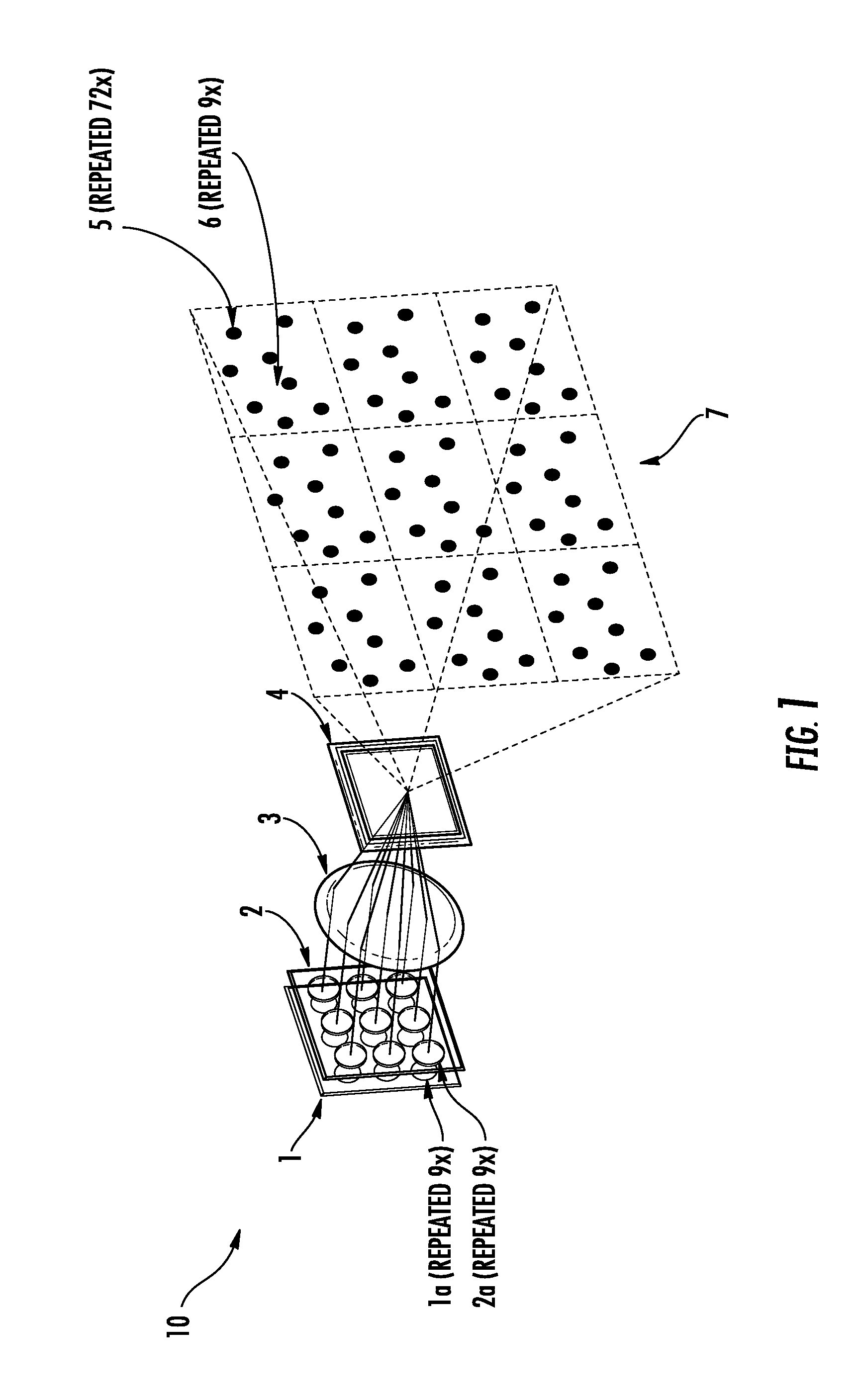
[0024] FIG. 1 graphically depicts elements of an optical pattern projector according to an exemplary embodiment of the present invention.
[0025] FIG. 2 schematically depicts a block diagram of a structured-light dimensioning system according to an exemplary embodiment of the present invention.
[0026] FIG. 3 depicts a flow chart of a method for creating a repeating optical pattern according to an exemplary embodiment of the present invention.
DETAILED DESCRIPTION
[0027] In one aspect, the present invention embraces an optical pattern projector for a structured-light dimensioning system that utilizes a standard laser array and a single diffractive optical element.
[0028] The exemplary optical pattern projector shown in Figure (FIG. 1 utilizes a plurality of light sources (i.e., lasers) arranged in an array to radiate light in the same direction.
[0029] An array of vertical cavity surface emitting lasers (i.e., VCSELs) are suitable for use as the optical pattern projector's 10 laser array 1 for a few reasons. First, the VCSEL array may be fabricated into a two-dimensional array using standard semiconductor materials and standard semiconductor fabrication techniques. Next, the low threshold current requirements of the VCSEL enable high-density arrays. Next, the VCSELs in the array typically radiate light in a direction that is perpendicular to the substrate (i.e., package), allowing for convenient alignment in a larger optical system. Finally, the light from a VSCEL (i.e., a "dot") is substantially circular, making it suitable for forming the optical patterns used for dimensioning.
[0030] The lasers 1a in the laser array 1 may be physically arranged in a specific geometry (e.g., rectangular grid, hexangular grid, etc.). Different array sizes are possible (e.g., 3.times.9) and depend on the pattern requirements for dimensioning (e.g., overall pattern size, replicated pattern frequency, etc.).
[0031] The lasers 1a in the laser array 1 are typically identical, each radiating light with a particular wavelength (e.g., 780-900 nanometers (nm)), a particular power, and (in some cases) a particular polarization.
[0032] The optical power from the laser array 1 is adjustable. For dimensioning applications, the optical power may be configured at levels considered safe for normal use at typical dimensioning ranges (e.g. 0.5-5 meters).
[0033] The lasers 1a in the laser array 1 may be electrically addressed individually or in groups and driven to generate either pulsed of continuous (i.e., CW) radiation. In an embodiment of the present invention, the lasers simultaneously radiate CW light for a period corresponding to the dimensioning process. In another embodiment of the present invention, a subset of the lasers in the laser array radiate CW light for a period corresponding to the dimensioning process.
[0034] A laser 1a in the laser array 1 typically radiates light divergently. This light may formed into a collimated laser beam using a small lens (i.e., lenslet) positioned in front of the laser. Thus a lenslet array 2 including a plurality of lenslets 2a (e.g., one for each laser) may be positioned in front of the laser array 1 to form a plurality of collimated laser beams. The laser beams are co-directed and are typically co-linear. The lenslet array 2 typically includes identical lenslets 2a. The lenslets may be discrete. While single lens elements are typical, each lenslet 2a may utilize multiple optical elements (e.g., lenses, filters, etc.). The lenslet array may be formed from a common substrate using semiconductor-processing technology. In some embodiments, an opaque film may be applied to the areas between lenslets to block stray light.
[0035] The lenslet array 2 is positioned in front of laser array 1 at a distance determined by the lenslet characteristics (e.g., f-number) and the radiated light characteristics (e.g., a full pattern angle). The positioning may be accomplished by integrating the lenslet array 3 and the laser array 1 within a common package. Alternatively, the lenslet array 3 may be positioned in front of the laser array 1 using a separate mechanical structure. Fine mechanical adjustments in position of one or more lenslets (or VCSELs) may be possible. In a possible embodiment, this adjusting of the position of one or more lenslets may be used to change the projected pattern.
[0036] A lens 3 having a diameter large enough to capture all of the collimated laser beams is positioned in front of the lenslet array 2 to focus (i.e., redirect) the collimated laser beams (i.e., laser beams). Each laser beam is redirected by the lens 3 to a particular incident angle determined by the laser-beam's position within the laser array 1.
[0037] The lens 3 focuses the laser beams onto a diffractive optical element (DOE) 4, which is positioned at (or near) the focal plane of the lens 4. In a possible embodiment, the lens 3 is an f-theta lens. An f-theta lens provides a flat field as opposed to focusing light onto a spherical plane. An f-theta lens also provides a linear mapping of position/angle. These aspects may be desirable for creating the optical pattern.
[0038] The lens 3 may be fabricated using techniques known to those skilled in the art using materials transparent to the light radiation (e.g., glass, fused silica, polycarbonate, etc.). In some embodiments, the lens maybe coated with an antireflection coating to improve throughput, reduce reflections, and/or filter stray-light.
[0039] The optical pattern projector's DOE 4 diffracts a collimated laser beam in a plurality of beams. The plurality of beams form a sub-pattern of light spots (i.e., dots) 5 on a target.
[0040] As shown in FIG. 1, the DOE 4 receives a plurality of laser beams. Each laser beam creates an identical sub-pattern (e.g., a pattern of light spots). Each sub-pattern 6 typically includes the same pattern of light spots 5. The spots in the sub-pattern may be different sizes. The sub-pattern includes the number of light spots necessary for dimensioning. For example, in one possible embodiment, the sub-pattern 6 includes 3-15 light spots. In addition, the separation between dots 5 may be chosen so that no touching dots within the sub-pattern are allowed.
[0041] Sub-patterns 6 are projected onto a target (i.e., object) and combine to form an optical pattern 7 (i.e., structured-light pattern). The optical pattern's sub-patterns may be sized so that, for ranges expected in dimensioning (e.g., 0.5 to 4.5 meters), the sub-patterns 6 do not overlap. The distribution of the spots (i.e., dots) 5 in the sub-pattern may be chosen to insure that the optical pattern 7 is symmetrical relative to the center. Further, dots at the edges of a sub-pattern may be configured so that when combined with other sub-patterns do not form touching light spots.
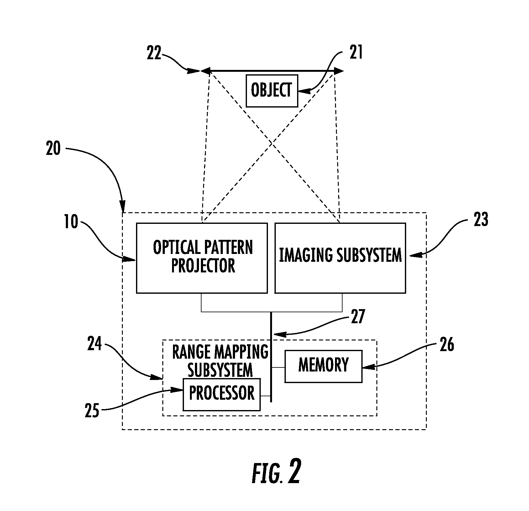
[0042] The optical pattern projector 10 thus far described may be part of a structured-light dimensioning system 20 as shown in FIG. 2. The structured-light dimensioning system 20 can measure the dimension of an object 21 (e.g., volume) placed in its field of view 22 by first projecting a known optical pattern onto the object 21.
[0043] Images of the object 21 and the optical pattern 7 may be captured using an imaging subsystem 23 positioned in proximity to the optical pattern projector (e.g., stereoscopically). The imaging subsystem 23 captures images of the object 21 and the projected light pattern 7. To accomplish this, the imaging subsystem 23 may use an imaging lens to render a real image of the imaging lens's field of view 22 onto an image sensor. This imaging lens field of view 22 overlaps at least partially with the projected light pattern 23. The image sensor may be a charge coupled device (i.e., CCD) or a sensor using complementary metal oxide semiconductor (i.e., CMOS) technology. The image sensor includes a plurality of pixels that sample the real image and convert intensity into an electronic signal.
[0044] A range mapping subsystem 24 having a processor (e.g., one or more controller, digital signal processor (DSP), application specific integrated circuit (ASIC), programmable gate array (PGA), and/or programmable logic controller (PLC)) configured by processor-executable instructions (i.e., software) stored in at least one non-transitory storage medium (i.e., memory) 26 (e.g., read-only memory (ROM), flash memory, and/or a hard-drive), can processes the captured images and measure any distortions to the optical pattern 7 (e.g., distortions to the pattern caused by the object). The distortions to the optical pattern may analyzed to produce a range image. A range image has pixels that spatially match the field of view, like an image, but that have grayscale values that correlate with range. The range image may be processed to determine the dimensions of the object 21.
[0045] The subsystems in the structured-light dimensioning system are connected via a couplers (e.g., wires or fibers), buses, and control lines to form an interconnection subsystem 27 that allows communication and interaction.
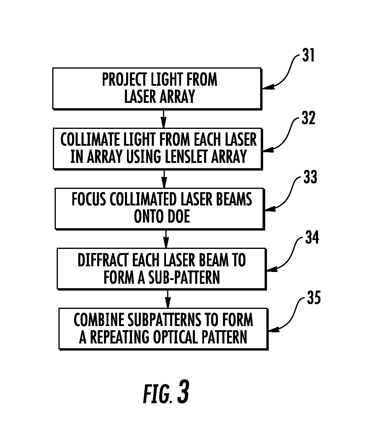
[0046] A method for creating a repeating optical pattern according to an exemplary embodiment of the present invention is shown in FIG. 3. The method includes the step of projecting light from a laser array 31. The laser array includes a square grid of co-directed lasers. The method also includes the step of collimating the light from each laser with a lenslet array 32. The method also includes the step of focusing the light from each laser beam onto a DOE using an f-theta lens 33. The f-theta lens focuses each laser beam along a particular incident angle determined by the laser beam's position in the square grid. Finally, the method includes the step of diffracting the light from each laser beam to form a sub-pattern 34. Each sub-pattern propagates along a particular angle that is determine by the incident angle of the particular laser beam. The sub-patterns combine to form a repeating optical pattern 35.
[0047] To supplement the present disclosure, this application incorporates entirely by reference the following commonly assigned patents, patent application publications, and patent applications:
To supplement the present disclosure, this application incorporates entirely by reference the following patents, patent application publications, and patent applications: [0048] U.S. Pat. No. 6,832,725; U.S. Pat. No. 7,128,266; [0049] U.S. Pat. No. 7,159,783; U.S. Pat. No. 7,413,127; [0050] U.S. Pat. No. 7,726,575; U.S. Pat. No. 8,294,969; [0051] U.S. Pat. No. 8,317,105; U.S. Pat. No. 8,322,622; [0052] U.S. Pat. No. 8,366,005; U.S. Pat. No. 8,371,507; [0053] U.S. Pat. No. 8,376,233; U.S. Pat. No. 8,381,979; [0054] U.S. Pat. No. 8,390,909; U.S. Pat. No. 8,408,464; [0055] U.S. Pat. No. 8,408,468; U.S. Pat. No. 8,408,469; [0056] U.S. Pat. No. 8,424,768; U.S. Pat. No. 8,448,863; [0057] U.S. Pat. No. 8,457,013; U.S. Pat. No. 8,459,557; [0058] U.S. Pat. No. 8,469,272; U.S. Pat. No. 8,474,712; [0059] U.S. Pat. No. 8,479,992; U.S. Pat. No. 8,490,877; [0060] U.S. Pat. No. 8,517,271; U.S. Pat. No. 8,523,076; [0061] U.S. Pat. No. 8,528,818; U.S. Pat. No. 8,544,737; [0062] U.S. Pat. No. 8,548,242; U.S. Pat. No. 8,548,420; [0063] U.S. Pat. No. 8,550,335; U.S. Pat. No. 8,550,354; [0064] U.S. Pat. No. 8,550,357; U.S. Pat. No. 8,556,174; [0065] U.S. Pat. No. 8,556,176; U.S. Pat. No. 8,556,177; [0066] U.S. Pat. No. 8,559,767; U.S. Pat. No. 8,599,957; [0067] U.S. Pat. No. 8,561,895; U.S. Pat. No. 8,561,903; [0068] U.S. Pat. No. 8,561,905; U.S. Pat. No. 8,565,107; [0069] U.S. Pat. No. 8,571,307; U.S. Pat. No. 8,579,200; [0070] U.S. Pat. No. 8,583,924; U.S. Pat. No. 8,584,945; [0071] U.S. Pat. No. 8,587,595; U.S. Pat. No. 8,587,697; [0072] U.S. Pat. No. 8,588,869; U.S. Pat. No. 8,590,789; [0073] U.S. Pat. No. 8,596,539; U.S. Pat. No. 8,596,542; [0074] U.S. Pat. No. 8,596,543; U.S. Pat. No. 8,599,271; [0075] U.S. Pat. No. 8,599,957; U.S. Pat. No. 8,600,158; [0076] U.S. Pat. No. 8,600,167; U.S. Pat. No. 8,602,309; [0077] U.S. Pat. No. 8,608,053; U.S. Pat. No. 8,608,071; [0078] U.S. Pat. No. 8,611,309; U.S. Pat. No. 8,615,487; [0079] U.S. Pat. No. 8,616,454; U.S. Pat. No. 8,621,123; [0080] U.S. Pat. No. 8,622,303; U.S. Pat. No. 8,628,013; [0081] U.S. Pat. No. 8,628,015; U.S. Pat. No. 8,628,016; [0082] U.S. Pat. No. 8,629,926; U.S. Pat. No. 8,630,491; [0083] U.S. Pat. No. 8,635,309; U.S. Pat. No. 8,636,200; [0084] U.S. Pat. No. 8,636,212; U.S. Pat. No. 8,636,215; [0085] U.S. Pat. No. 8,636,224; U.S. Pat. No. 8,638,806; [0086] U.S. Pat. No. 8,640,958; U.S. Pat. No. 8,640,960; [0087] U.S. Pat. No. 8,643,717; U.S. Pat. No. 8,646,692; [0088] U.S. Pat. No. 8,646,694; U.S. Pat. No. 8,657,200; [0089] U.S. Pat. No. 8,659,397; U.S. Pat. No. 8,668,149; [0090] U.S. Pat. No. 8,678,285; U.S. Pat. No. 8,678,286; [0091] U.S. Pat. No. 8,682,077; U.S. Pat. No. 8,687,282; [0092] U.S. Pat. No. 8,692,927; U.S. Pat. No. 8,695,880; [0093] U.S. Pat. No. 8,698,949; U.S. Pat. No. 8,717,494; [0094] U.S. Pat. No. 8,717,494; U.S. Pat. No. 8,720,783; [0095] U.S. Pat. No. 8,723,804; U.S. Pat. No. 8,723,904; [0096] U.S. Pat. No. 8,727,223; U.S. Pat. No. D702,237; [0097] U.S. Pat. No. 8,740,082; U.S. Pat. No. 8,740,085; [0098] U.S. Pat. No. 8,746,563; U.S. Pat. No. 8,750,445; [0099] U.S. Pat. No. 8,752,766; U.S. Pat. No. 8,756,059; [0100] U.S. Pat. No. 8,757,495; U.S. Pat. No. 8,760,563; [0101] U.S. Pat. No. 8,763,909; U.S. Pat. No. 8,777,108; [0102] U.S. Pat. No. 8,777,109; U.S. Pat. No. 8,779,898; [0103] U.S. Pat. No. 8,781,520; U.S. Pat. No. 8,783,573; [0104] U.S. Pat. No. 8,789,757; U.S. Pat. No. 8,789,758; [0105] U.S. Pat. No. 8,789,759; U.S. Pat. No. 8,794,520; [0106] U.S. Pat. No. 8,794,522; U.S. Pat. No. 8,794,526; [0107] U.S. Pat. No. 8,798,367; U.S. Pat. No. 8,807,431; [0108] U.S. Pat. No. 8,807,432; U.S. Pat. No. 8,820,630; [0109] International Publication No. 2013/163789; [0110] International Publication No. 2013/173985; [0111] International Publication No. 2014/019130; [0112] International Publication No. 2014/110495; [0113] U.S. Patent Application Publication No. 2008/0185432; [0114] U.S. Patent Application Publication No. 2009/0134221; [0115] U.S. Patent Application Publication No. 2010/0177080; [0116] U.S. Patent Application Publication No. 2010/0177076; [0117] U.S. Patent Application Publication No. 2010/0177707; [0118] U.S. Patent Application Publication No. 2010/0177749; [0119] U.S. Patent Application Publication No. 2011/0202554; [0120] U.S. Patent Application Publication No. 2012/0111946; [0121] U.S. Patent Application Publication No. 2012/0138685; [0122] U.S. Patent Application Publication No. 2012/0168511; [0123] U.S. Patent Application Publication No. 2012/0168512; [0124] U.S. Patent Application Publication No. 2012/0193423; [0125] U.S. Patent Application Publication No. 2012/0203647; [0126] U.S. Patent Application Publication No. 2012/0223141; [0127] U.S. Patent Application Publication No. 2012/0228382; [0128] U.S. Patent Application Publication No. 2012/0248188; [0129] U.S. Patent Application Publication No. 2013/0043312; [0130] U.S. Patent Application Publication No. 2013/0056285; [0131] U.S. Patent Application Publication No. 2013/0070322; [0132] U.S. Patent Application Publication No. 2013/0075168; [0133] U.S. Patent Application Publication No. 2013/0082104; [0134] U.S. Patent Application Publication No. 2013/0175341; [0135] U.S. Patent Application Publication No. 2013/0175343; [0136] U.S. Patent Application Publication No. 2013/0200158; [0137] U.S. Patent Application Publication No. 2013/0256418; [0138] U.S. Patent Application Publication No. 2013/0257744; [0139] U.S. Patent Application Publication No. 2013/0257759; [0140] U.S. Patent Application Publication No. 2013/0270346; [0141] U.S. Patent Application Publication No. 2013/0278425; [0142] U.S. Patent Application Publication No. 2013/0287258; [0143] U.S. Patent Application Publication No. 2013/0292475; [0144] U.S. Patent Application Publication No. 2013/0292477; [0145] U.S. Patent Application Publication No. 2013/0293539; [0146] U.S. Patent Application Publication No. 2013/0293540; [0147] U.S. Patent Application Publication No. 2013/0306728; [0148] U.S. Patent Application Publication No. 2013/0306730; [0149] U.S. Patent Application Publication No. 2013/0306731; [0150] U.S. Patent Application Publication No. 2013/0307964; [0151] U.S. Patent Application Publication No. 2013/0308625; [0152] U.S. Patent Application Publication No. 2013/0313324; [0153] U.S. Patent Application Publication No. 2013/0313325; [0154] U.S. Patent Application Publication No. 2013/0341399; [0155] U.S. Patent Application Publication No. 2013/0342717; [0156] U.S. Patent Application Publication No. 2014/0001267; [0157] U.S. Patent Application Publication No. 2014/0002828; [0158] U.S. Patent Application Publication No. 2014/0008430; [0159] U.S. Patent Application Publication No. 2014/0008439; [0160] U.S. Patent Application Publication No. 2014/0025584; [0161] U.S. Patent Application Publication No. 2014/0027518; [0162] U.S. Patent Application Publication No. 2014/0034734; [0163] U.S. Patent Application Publication No. 2014/0036848; [0164] U.S. Patent Application Publication No. 2014/0039693; [0165] U.S. Patent Application Publication No. 2014/0042814; [0166] U.S. Patent Application Publication No. 2014/0049120; [0167] U.S. Patent Application Publication No. 2014/0049635; [0168] U.S. Patent Application Publication No. 2014/0061305; [0169] U.S. Patent Application Publication No. 2014/0061306; [0170] U.S. Patent Application Publication No. 2014/0063289; [0171] U.S. Patent Application Publication No. 2014/0066136; [0172] U.S. Patent Application Publication No. 2014/0067692; [0173] U.S. Patent Application Publication No. 2014/0070005; [0174] U.S. Patent Application Publication No. 2014/0071840; [0175] U.S. Patent Application Publication No. 2014/0074746; [0176] U.S. Patent Application Publication No. 2014/0075846; [0177] U.S. Patent Application Publication No. 2014/0076974; [0178] U.S. Patent Application Publication No. 2014/0078341; [0179] U.S. Patent Application Publication No. 2014/0078342; [0180] U.S. Patent Application Publication No. 2014/0078345; [0181] U.S. Patent Application Publication No. 2014/0084068; [0182] U.S. Patent Application Publication No. 2014/0097249; [0183] U.S. Patent Application Publication No. 2014/0098792; [0184] U.S. Patent Application Publication No. 2014/0100774; [0185] U.S. Patent Application Publication No. 2014/0100813; [0186] U.S. Patent Application Publication No. 2014/0103115; [0187] U.S. Patent Application Publication No. 2014/0104413; [0188] U.S. Patent Application Publication No. 2014/0104414; [0189] U.S. Patent Application Publication No. 2014/0104416; [0190] U.S. Patent Application Publication No. 2014/0104451; [0191] U.S. Patent Application Publication No. 2014/0106594; [0192] U.S. Patent Application Publication No. 2014/0106725; [0193] U.S. Patent Application Publication No. 2014/0108010; [0194] U.S. Patent Application Publication No. 2014/0108402; [0195] U.S. Patent Application Publication No. 2014/0108682; [0196] U.S. Patent Application Publication No. 2014/0110485; [0197] U.S. Patent Application Publication No. 2014/0114530; [0198] U.S. Patent Application Publication No. 2014/0124577; [0199] U.S. Patent Application Publication No. 2014/0124579; [0200] U.S. Patent Application Publication No. 2014/0125842; [0201] U.S. Patent Application Publication No. 2014/0125853; [0202] U.S. Patent Application Publication No. 2014/0125999; [0203] U.S. Patent Application Publication No. 2014/0129378; [0204] U.S. Patent Application Publication No. 2014/0131438; [0205] U.S. Patent Application Publication No. 2014/0131441; [0206] U.S. Patent Application Publication No. 2014/0131443; [0207] U.S. Patent Application Publication No. 2014/0131444; [0208] U.S. Patent Application Publication No. 2014/0131445; [0209] U.S. Patent Application Publication No. 2014/0131448; [0210] U.S. Patent Application Publication No. 2014/0133379; [0211] U.S. Patent Application Publication No. 2014/0136208; [0212] U.S. Patent Application Publication No. 2014/0140585; [0213] U.S. Patent Application Publication No. 2014/0151453; [0214] U.S. Patent Application Publication No. 2014/0152882; [0215] U.S. Patent Application Publication No. 2014/0158770; [0216] U.S. Patent Application Publication No. 2014/0159869; [0217] U.S. Patent Application Publication No. 2014/0160329; [0218] U.S. Patent Application Publication No. 2014/0166755; [0219] U.S. Patent Application Publication No. 2014/0166757; [0220] U.S. Patent Application Publication No. 2014/0166759; [0221] U.S. Patent Application Publication No. 2014/0166760; [0222] U.S. Patent Application Publication No. 2014/0166761; [0223] U.S. Patent Application Publication No. 2014/0168787; [0224] U.S. Patent Application Publication No. 2014/0175165; [0225] U.S. Patent Application Publication No. 2014/0175169; [0226] U.S. Patent Application Publication No. 2014/0175172; [0227] U.S. Patent Application Publication No. 2014/0175174; [0228] U.S. Patent Application Publication No. 2014/0191644; [0229] U.S. Patent Application Publication No. 2014/0191913; [0230] U.S. Patent Application Publication No. 2014/0197238; [0231] U.S. Patent Application Publication No. 2014/0197239; [0232] U.S. Patent Application Publication No. 2014/0197304; [0233] U.S. Patent Application Publication No. 2014/0203087; [0234] U.S. Patent Application Publication No. 2014/0204268; [0235] U.S. Patent Application Publication No. 2014/0214631; [0236] U.S. Patent Application Publication No. 2014/0217166; [0237] U.S. Patent Application Publication No. 2014/0217180; [0238] U.S. patent application Ser. No. 13/367,978 for a Laser Scanning Module Employing an Elastomeric U-Hinge Based Laser Scanning Assembly, filed Feb. 7, 2012 (Feng et al.); [0239] U.S. patent application Ser. No. 29/436,337 for an Electronic Device, filed Nov. 5, 2012 (Fitch et al.); [0240] U.S. patent application Ser. No. 13/771,508 for an Optical Redirection Adapter, filed Feb. 20, 2013 (Anderson); [0241] U.S. patent application Ser. No. 13/852,097 for a System and Method for Capturing and Preserving Vehicle Event Data, filed Mar. 28, 2013 (Barker et al.); [0242] U.S. patent application Ser. No. 13/902,110 for a System and Method for Display of Information Using a Vehicle-Mount Computer, filed May 24, 2013 (Hollifield); [0243] U.S. patent application Ser. No. 13/902,144, for a System and Method for Display of Information Using a Vehicle-Mount Computer, filed May 24, 2013 (Chamberlin); [0244] U.S. patent application Ser. No. 13/902,242 for a System For Providing A Continuous Communication Link With A Symbol Reading Device, filed May 24, 2013 (Smith et al.); [0245] U.S. patent application Ser. No. 13/912,262 for a Method of Error Correction for 3D Imaging Device, filed Jun. 7, 2013 (Jovanovski et al.); [0246] U.S. patent application Ser. No. 13/912,702 for a System and Method for Reading Code Symbols at Long Range Using Source Power Control, filed Jun. 7, 2013 (Xian et al.); [0247] U.S. patent application Ser. No. 29/458,405 for an Electronic Device, filed Jun. 19, 2013 (Fitch et al.); [0248] U.S. patent application Ser. No. 13/922,339 for a System and Method for Reading Code Symbols Using a Variable Field of View, filed Jun. 20, 2013 (Xian et al.); [0249] U.S. patent application Ser. No. 13/927,398 for a Code Symbol Reading System Having Adaptive Autofocus, filed Jun. 26, 2013 (Todeschini); [0250] U.S. patent application Ser. No. 13/930,913 for a Mobile Device Having an Improved User Interface for Reading Code Symbols, filed Jun. 28, 2013 (Gelay et al.); [0251] U.S. patent application Ser. No. 29/459,620 for an Electronic Device Enclosure, filed Jul. 2, 2013 (London et al.); [0252] U.S. patent application Ser. No. 29/459,681 for an Electronic Device Enclosure, filed Jul. 2, 2013 (Chaney et al.); [0253] U.S. patent application Ser. No. 13/933,415 for an Electronic Device Case, filed Jul. 2, 2013 (London et al.); [0254] U.S. patent application Ser. No. 29/459,785 for a Scanner and Charging Base, filed Jul. 3, 2013 (Fitch et al.); [0255] U.S. patent application Ser. No. 29/459,823 for a Scanner, filed Jul. 3, 2013 (Zhou et al.); [0256] U.S. patent application Ser. No. 13/947,296 for a System and Method for Selectively Reading Code Symbols, filed Jul. 22, 2013 (Rueblinger et al.); [0257] U.S. patent application Ser. No. 13/950,544 for a Code Symbol Reading System Having Adjustable Object Detection, filed Jul. 25, 2013 (Jiang); [0258] U.S. patent application Ser. No. 13/961,408 for a Method for Manufacturing Laser Scanners, filed Aug. 7, 2013 (Saber et al.); [0259] U.S. patent application Ser. No. 14/018,729 for a Method for Operating a Laser Scanner, filed Sep. 5, 2013 (Feng et al.); [0260] U.S. patent application Ser. No. 14/019,616 for a Device Having Light Source to Reduce Surface Pathogens, filed Sep. 6, 2013 (Todeschini); [0261] U.S. patent application Ser. No. 14/023,762 for a Handheld Indicia Reader Having Locking Endcap, filed Sep. 11, 2013 (Gannon); [0262] U.S. patent application Ser. No. 14/035,474 for Augmented-Reality Signature Capture, filed Sep. 24, 2013 (Todeschini);
[0263] U.S. patent application Ser. No. 29/468,118 for an Electronic Device Case, filed Sep. 26, 2013 (Oberpriller et al.); [0264] U.S. patent application Ser. No. 14/055,234 for Dimensioning System, filed Oct. 16, 2013 (Fletcher); [0265] U.S. patent application Ser. No. 14/053,314 for Indicia Reader, filed Oct. 14, 2013 (Huck); [0266] U.S. patent application Ser. No. 14/065,768 for Hybrid System and Method for Reading Indicia, filed Oct. 29, 2013 (Meier et al.); [0267] U.S. patent application Ser. No. 14/074,746 for Self-Checkout Shopping System, filed Nov. 8, 2013 (Hejl et al.); [0268] U.S. patent application Ser. No. 14/074,787 for Method and System for Configuring Mobile Devices via NFC Technology, filed Nov. 8, 2013 (Smith et al.); [0269] U.S. patent application Ser. No. 14/087,190 for Optimal Range Indicators for Bar Code Validation, filed Nov. 22, 2013 (Hejl); [0270] U.S. patent application Ser. No. 14/094,087 for Method and System for Communicating Information in an Digital Signal, filed Dec. 2, 2013 (Peake et al.); [0271] U.S. patent application Ser. No. 14/101,965 for High Dynamic-Range Indicia Reading System, filed Dec. 10, 2013 (Xian); [0272] U.S. patent application Ser. No. 14/150,393 for Indicia-reader Having Unitary Construction Scanner, filed Jan. 8, 2014 (Colavito et al.); [0273] U.S. patent application Ser. No. 14/154,207 for Laser Barcode Scanner, filed Jan. 14, 2014 (Hou et al.); [0274] U.S. patent application Ser. No. 14/165,980 for System and Method for Measuring Irregular Objects with a Single Camera filed Jan. 28, 2014 (Li et al.); [0275] U.S. patent application Ser. No. 14/166,103 for Indicia Reading Terminal Including Optical Filter filed Jan. 28, 2014 (Lu et al.); [0276] U.S. patent application Ser. No. 14/200,405 for Indicia Reader for Size-Limited Applications filed Mar. 7, 2014 (Feng et al.); [0277] U.S. patent application Ser. No. 14/231,898 for Hand-Mounted Indicia-Reading Device with Finger Motion Triggering filed Apr. 1, 2014 (Van Horn et al.); [0278] U.S. patent application Ser. No. 14/250,923 for Reading Apparatus Having Partial Frame Operating Mode filed Apr. 11, 2014, (Deng et al.); [0279] U.S. patent application Ser. No. 14/257,174 for Imaging Terminal Having Data Compression filed Apr. 21, 2014, (Barber et al.); [0280] U.S. patent application Ser. No. 14/257,364 for Docking System and Method Using Near Field Communication filed Apr. 21, 2014 (Showering); [0281] U.S. patent application Ser. No. 14/264,173 for Autofocus Lens System for Indicia Readers filed Apr. 29, 2014 (Ackley et al.); [0282] U.S. patent application Ser. No. 14/274,858 for Mobile Printer with Optional Battery Accessory filed May 12, 2014 (Marty et al.); [0283] U.S. patent application Ser. No. 14/277,337 for MULTIPURPOSE OPTICAL READER, filed May 14, 2014 (Jovanovski et al.); [0284] U.S. patent application Ser. No. 14/283,282 for TERMINAL HAVING ILLUMINATION AND FOCUS CONTROL filed May 21, 2014 (Liu et al.); [0285] U.S. patent application Ser. No. 14/300,276 for METHOD AND SYSTEM FOR CONSIDERING INFORMATION ABOUT AN EXPECTED RESPONSE WHEN PERFORMING SPEECH RECOGNITION, filed Jun. 10, 2014 (Braho et al.); [0286] U.S. patent application Ser. No. 14/305,153 for INDICIA READING SYSTEM EMPLOYING DIGITAL GAIN CONTROL filed Jun. 16, 2014 (Xian et al.); [0287] U.S. patent application Ser. No. 14/310,226 for AUTOFOCUSING OPTICAL IMAGING DEVICE filed Jun. 20, 2014 (Koziol et al.); [0288] U.S. patent application Ser. No. 14/327,722 for CUSTOMER FACING IMAGING SYSTEMS AND METHODS FOR OBTAINING IMAGES filed Jul. 10, 2014 (Oberpriller et al,); [0289] U.S. patent application Ser. No. 14/327,827 for a MOBILE-PHONE ADAPTER FOR ELECTRONIC TRANSACTIONS, filed Jul. 10, 2014 (Hejl); [0290] U.S. patent application Ser. No. 14/329,303 for CELL PHONE READING MODE USING IMAGE TIMER filed Jul. 11, 2014 (Coyle); [0291] U.S. patent application Ser. No. 14/333,588 for SYMBOL READING SYSTEM WITH INTEGRATED SCALE BASE filed Jul. 17, 2014 (Barten); [0292] U.S. patent application Ser. No. 14/334,934 for a SYSTEM AND METHOD FOR INDICIA VERIFICATION, filed Jul. 18, 2014 (Hejl); [0293] U.S. patent application Ser. No. 14/336,188 for METHOD OF AND SYSTEM FOR DETECTING OBJECT WEIGHING INTERFERENCES, Filed Jul. 21, 2014 (Amundsen et al.); [0294] U.S. patent application Ser. No. 14/339,708 for LASER SCANNING CODE SYMBOL READING SYSTEM, filed Jul. 24, 2014 (Xian et al.); [0295] U.S. patent application Ser. No. 14/340,627 for an AXIALLY REINFORCED FLEXIBLE SCAN ELEMENT, filed Jul. 25, 2014 (Rueblinger et al.); [0296] U.S. patent application Ser. No. 14/340,716 for an OPTICAL IMAGER AND METHOD FOR CORRELATING A MEDICATION PACKAGE WITH A PATIENT, filed Jul. 25, 2014 (Ellis); [0297] U.S. patent application Ser. No. 14/342,544 for Imaging Based Barcode Scanner Engine with Multiple Elements Supported on a Common Printed Circuit Board filed Mar. 4, 2014 (Liu et al.); [0298] U.S. patent application Ser. No. 14/345,735 for Optical Indicia Reading Terminal with Combined Illumination filed Mar. 19, 2014 (Ouyang); [0299] U.S. patent application Ser. No. 14/336,188 for METHOD OF AND SYSTEM FOR DETECTING OBJECT WEIGHING INTERFERENCES, Filed Jul. 21, 2014 (Amundsen et al.); [0300] U.S. patent application Ser. No. 14/355,613 for Optical Indicia Reading Terminal with Color Image Sensor filed May 1, 2014 (Lu et al.); [0301] U.S. patent application Ser. No. 14/370,237 for WEB-BASED SCAN-TASK ENABLED SYSTEM AND METHOD OF AND APPARATUS FOR DEVELOPING AND DEPLOYING THE SAME ON A CLIENT-SERVER NETWORK filed Jul. 2, 2014 (Chen et al.); [0302] U.S. patent application Ser. No. 14/370,267 for INDUSTRIAL DESIGN FOR CONSUMER DEVICE BASED SCANNING AND MOBILITY, filed Jul. 2, 2014 (Ma et al.); [0303] U.S. patent application Ser. No. 14/376,472, for an ENCODED INFORMATION READING TERMINAL INCLUDING HTTP SERVER, filed Aug. 4, 2014 (Lu); [0304] U.S. patent application Ser. No. 14/379,057 for METHOD OF USING CAMERA SENSOR INTERFACE TO TRANSFER MULTIPLE CHANNELS OF SCAN DATA USING AN IMAGE FORMAT filed Aug. 15, 2014 (Wang et al.); [0305] U.S. patent application Ser. No. 14/452,697 for INTERACTIVE INDICIA READER, filed Aug. 6, 2014 (Todeschini); [0306] U.S. patent application Ser. No. 14/453,019 for DIMENSIONING SYSTEM WITH GUIDED ALIGNMENT, filed Aug. 6, 2014 (Li et al.); [0307] U.S. patent application Ser. No. 14/460,387 for APPARATUS FOR DISPLAYING BAR CODES FROM LIGHT EMITTING DISPLAY SURFACES filed Aug. 15, 2014 (Van Horn et al.); [0308] U.S. patent application Ser. No. 14/460,829 for ENCODED INFORMATION READING TERMINAL WITH WIRELESS PATH SELECTON CAPABILITY, filed Aug. 15, 2014 (Wang et al.); [0309] U.S. patent application Ser. No. 14/462,801 for MOBILE COMPUTING DEVICE WITH DATA COGNITION SOFTWARE, filed on Aug. 19, 2014 (Todeschini et al.); [0310] U.S. patent application Ser. No. 14/446,387 for INDICIA READING TERMINAL PROCESSING PLURALITY OF FRAMES OF IMAGE DATA RESPONSIVELY TO TRIGGER SIGNAL ACTIVATION filed Jul. 30, 2014 (Wang et al.); [0311] U.S. patent application Ser. No. 14/446,391 for MULTIFUNCTION POINT OF SALE APPARATUS WITH OPTICAL SIGNATURE CAPTURE filed Jul. 30, 2014 (Good et al.); [0312] U.S. patent application Ser. No. 29/486,759 for an Imaging Terminal, filed Apr. 2, 2014 (Oberpriller et al.); [0313] U.S. patent application Ser. No. 29/492,903 for an INDICIA SCANNER, filed Jun. 4, 2014 (Zhou et al.); and [0314] U.S. patent application Ser. No. 29/494,725 for an IN-COUNTER BARCODE SCANNER, filed Jun. 24, 2014 (Oberpriller et al.).
[0315] In the specification and/or figures, typical embodiments of the invention have been disclosed. The present invention is not limited to such exemplary embodiments. The use of the term "and/or" includes any and all combinations of one or more of the associated listed items. The figures are schematic representations and so are not necessarily drawn to scale. Unless otherwise noted, specific terms have been used in a generic and descriptive sense and not for purposes of limitation.
* * * * *
D00000
D00001
D00002
D00003
XML
uspto.report is an independent third-party trademark research tool that is not affiliated, endorsed, or sponsored by the United States Patent and Trademark Office (USPTO) or any other governmental organization. The information provided by uspto.report is based on publicly available data at the time of writing and is intended for informational purposes only.
While we strive to provide accurate and up-to-date information, we do not guarantee the accuracy, completeness, reliability, or suitability of the information displayed on this site. The use of this site is at your own risk. Any reliance you place on such information is therefore strictly at your own risk.
All official trademark data, including owner information, should be verified by visiting the official USPTO website at www.uspto.gov. This site is not intended to replace professional legal advice and should not be used as a substitute for consulting with a legal professional who is knowledgeable about trademark law.