Remote Radio Head Unit System With Wideband Power Amplifier And Method
Wang; Chengxun ; et al.
U.S. patent application number 14/754908 was filed with the patent office on 2015-12-31 for remote radio head unit system with wideband power amplifier and method. The applicant listed for this patent is Dali Systems Co. Ltd.. Invention is credited to Shawn Patrick Stapleton, Chengxun Wang.
| Application Number | 20150382363 14/754908 |
| Document ID | / |
| Family ID | 47729603 |
| Filed Date | 2015-12-31 |


| United States Patent Application | 20150382363 |
| Kind Code | A1 |
| Wang; Chengxun ; et al. | December 31, 2015 |
REMOTE RADIO HEAD UNIT SYSTEM WITH WIDEBAND POWER AMPLIFIER AND METHOD
Abstract
A remote radio head unit (RRU) system for multiple operating frequency bands, multi-channels, driven by a single or more wide band power amplifiers. More specifically, the present invention enables multiple-bands RRU to use fewer power amplifiers in order to reduce size and cost of the multi-band RRU. The present invention is based on the method of using duplexers and/or interference cancellation system technique to increase the isolation between the transmitter signal and receiver signal of the RRU.
| Inventors: | Wang; Chengxun; (Shenzhen, CN) ; Stapleton; Shawn Patrick; (Burnaby, CA) | ||||||||||
| Applicant: |
|
||||||||||
|---|---|---|---|---|---|---|---|---|---|---|---|
| Family ID: | 47729603 | ||||||||||
| Appl. No.: | 14/754908 | ||||||||||
| Filed: | June 30, 2015 |
Related U.S. Patent Documents
| Application Number | Filing Date | Patent Number | ||
|---|---|---|---|---|
| 14248597 | Apr 9, 2014 | 9106453 | ||
| 14754908 | ||||
| 12928933 | Dec 21, 2010 | 8730786 | ||
| 14248597 | ||||
| 61288840 | Dec 21, 2009 | |||
| Current U.S. Class: | 370/329 |
| Current CPC Class: | H03F 3/245 20130101; H04B 1/40 20130101; H03F 2200/294 20130101; H03F 2200/111 20130101; H03F 2200/321 20130101; H04B 1/006 20130101; H04B 1/10 20130101; H04B 1/0053 20130101; H03F 1/0277 20130101; H04B 1/0067 20130101; H04B 1/525 20130101; H04B 1/123 20130101; H03F 3/72 20130101; H04B 1/0057 20130101; H03F 3/19 20130101; H03F 2203/7209 20130101 |
| International Class: | H04W 72/08 20060101 H04W072/08; H04W 72/04 20060101 H04W072/04 |
Claims
1. An interference mitigation system for improving isolation between transmitters and receivers in wireless communications systems comprising: a transmitter that transmits a transmit signal during a first time slot while a switch is in a first position; a feedback coupler that generates a feedback signal based on the transmit signal, wherein a characteristic of the feedback signal is representative of a characteristic of the transmit signal, an interference cancellation unit that processes the feedback signal to generate a processed signal; a receiver that receives an intake signal during a second time slot while the switch is in a second position, wherein the intake signal includes a first component from a signal received by the receiver and a second component from interference from the transmit signal, wherein whether the switch is in the first position or the second position is based on a time-division multiplexing technique; and a combiner that combines the intake signal received with the processed signal to generate a combined signal.
Description
RELATED APPLICATIONS
[0001] This application is a continuation of U.S. patent application Ser. No. 14/248,597, filed Apr. 4, 2014, titled REMOTE RADIO HEAD UNIT SYSTEM WITH WIDEBAND POWER AMPLIFIER AND METHOD, which is a continuation of U.S. patent application Ser. No. 12/928,933, filed Dec. 21, 2010, titled REMOTE RADIO HEAD UNIT SYSTEM WITH WIDEBAND POWER AMPLIFIER AND METHOD, which claims the benefit of U.S. Provisional Application No. 61/288,840, filed Dec. 21, 2009, titled REMOTE RADIO HEAD UNIT SYSTEM WITH WIDEBAND POWER AMPLIFIER AND METHOD and naming as inventors Chengxun Wang and Shawn Patrick Stapleton. Each of these applications is hereby incorporated by reference for all purposes.
FIELD OF THE INVENTION
[0002] The present invention generally relates to wireless communication systems using power amplifiers and remote radio head units (RRU or RRH). More specifically, the present invention relates to RRU which are part of a distributed base station in which all radio-related functions are contained in a small single unit that can be deployed in a location remote from the main unit.
BACKGROUND OF THE INVENTION
[0003] Wireless and mobile network operators face the continuing challenge of building networks that effectively manage high data-traffic growth rates. Mobility and an increased level of multimedia content for end users require end-to-end network adaptations that support both new services and the increased demand for broadband and flat-rate Internet access. In addition, network operators must consider the most cost-effective solutions to expand network capacity and evolution towards 4G and beyond.
[0004] Wireless and mobile technology standards are evolving towards higher bandwidth requirements for both peak rates and cell throughput growth. The latest standards supporting this are HSPA+, WiMAX, TD-SCDMA and LTE. The network upgrades required to deploy networks based on these standards must balance the limited availability of new spectrum, leverage existing spectrum, and ensure operation of all desired standards. This all must take place at the same time during the transition phase, which usually spans many years.
[0005] Distributed open base station architecture concepts have evolved in parallel with the evolution of the standards to provide a flexible, cheaper, and more scalable modular environment for managing the radio access evolution. For example, the Open Base Station Architecture Initiative (OBSAI), the Common Public Radio Interface (CPRI), and the IR Interface standards introduced standardized interfaces separating the Base Station server and the remote radio head part of a base station by an optical fiber.
[0006] The RRU concept is a fundamental part of a state-of-the-art base station architecture. 2G/3G/4G base stations are typically connected to RRUs over optical fibers. Either CPRI, OBSAI or IR Interfaces may be used to carry data to the RRH to cover a three-sector cell. The RRU incorporates a large number of digital interfacing and processing functions. Traditionally, a multi-channel RRU means that multiple antennas are used, typically with two power amplifiers for two distinct bands. A duplexer is used to combine the two power amplifier outputs. Switches are used to isolate the transmit signals from the received signals as occurs in a Time Division Synchronous Code Division Multiple Access (TD-SCDMA) modulation. To extent the prior art architecture to multiple bands (i.e., two or more bands) implementation would consist of adding additional channelized power amplifiers in parallel. The output of the additional power amplifiers is typically combined in an N by 1 duplexer and fed to a single antenna.
[0007] While conventional RRU architecture offers sonic benefits, RRUs to date are power-inefficient, costly and inflexible. Further, their poor DC-to-RF power conversion ensures that they will have a large mechanical housing. In addition, current RRU designs are inflexible. As standards evolve, there is a need for multi-band RRUs that can accommodate two or more operating channels using a single wideband power amplifier. This creates an isolation problem at the individual receivers because the wideband power amplifier is always turned on. Isolation between the wideband transmitter and receivers is a problem with any modulation standard (HSPA+, WiMAX, LTE, etc.) when multi-band RRUs are developed using a single power amplifier. This is a common problem for all communication systems that utilize a wideband power amplifier in a multi-band scenario.
SUMMARY OF THE INVENTION
[0008] Accordingly, the present invention has been made in view of the above problems, and it is an object of the present invention to provide a high performance and cost effective technique for implementing RRU systems that service multi-frequency bands. Further, the present disclosure enables a RRU to be field-reconfigurable, and supports multi-modulation schemes (modulation agnostic), multi-carriers, multi-frequency bands, and multi-channels. The present invention also serves multi-frequency bands within a single RRU to economize the cost of radio network deployment. In particular, the present invention resolves an isolation issue for a RRU with fewer power amplifiers than the number of operating frequency bands. Multi-mode radios capable of operating according to GSM, HSPA, LTE, TD-SCDMA and WiMAX standards and advanced software configurability are key features in the deployment of more flexible and energy-efficient radio networks.
[0009] The present invention achieves the above objects using techniques generally based on methods and techniques for maximizing the isolation between the transmitted signal (Tx Signal) and the received signal (Rx Signal). The Tx Signal may comprise noise generated at the output of the power amplifier or it may comprise an unwanted transmitter band leaking into the receiver. With the use of the present invention, conventional RRU's can be extended to a multi-band and multi-channel configuration. Multi-band means that more than one frequency bands are used in the RRU and multichannel means that more than one output antenna is used. Various embodiments of the invention are disclosed.
[0010] An embodiment of the present invention utilizes duplexers, switches and circulators to maximize the isolation between the transmitter and receiver. Another embodiment of the present invention utilizes an Interference Cancellation System (ICS) together with duplexers, switches and circulators.
[0011] Applications of the present invention are suitable for use with all wireless base-stations, remote radio heads, distributed base stations, distributed antenna systems, access points, repeaters, mobile equipment and wireless terminals, portable wireless devices, and other wireless communication systems such as microwave and satellite communications. The present invention is also field upgradable through a link such as an Ethernet connection to a remote computing center.
BRIEF DESCRIPTION OF THE DRAWINGS
[0012] Further objects and advantages of the present invention can be more fully understood from the following detailed description taken in conjunction with the accompanying drawings in which:
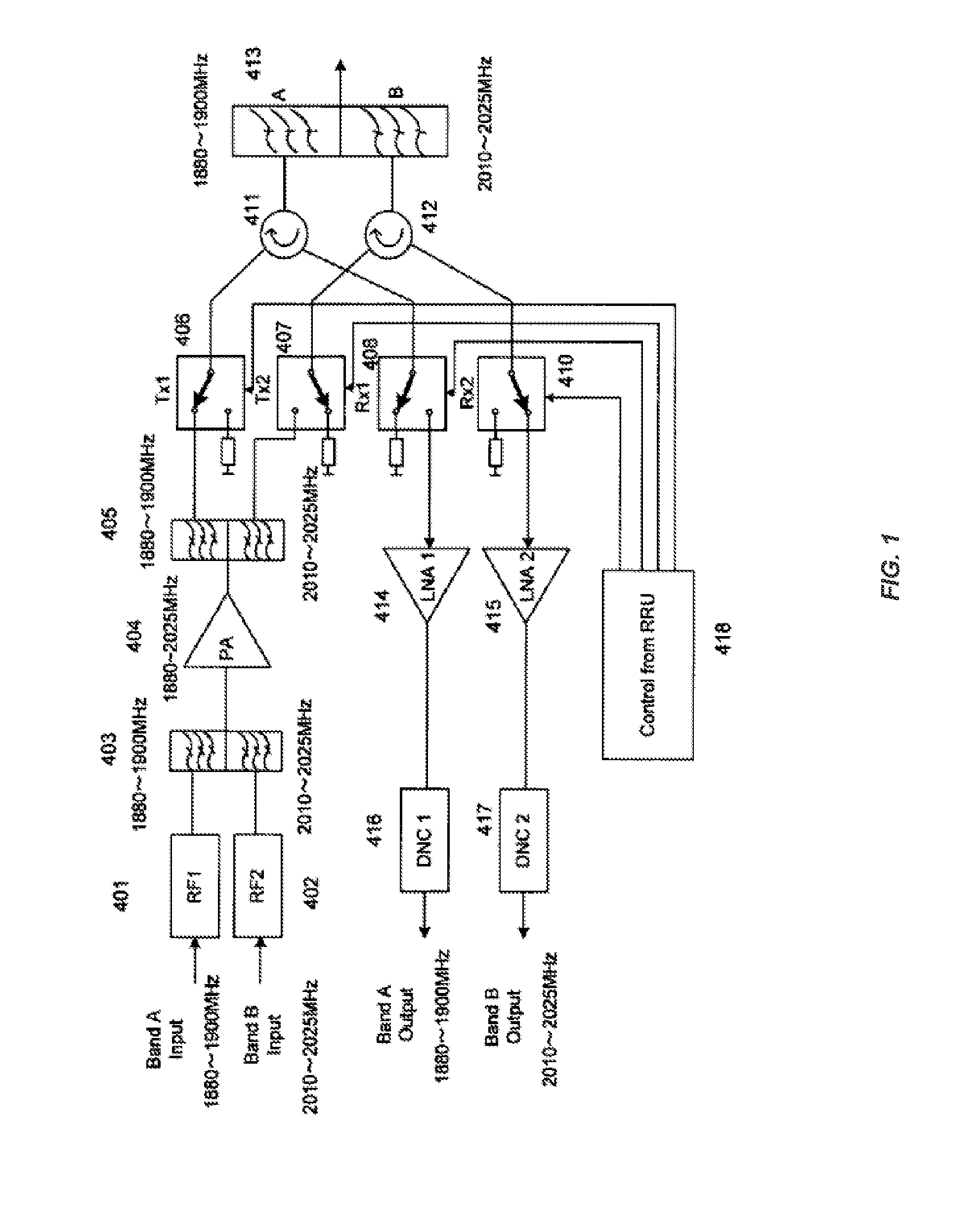
[0013] FIG. 1 is a block diagram of a TD-SCDMA dual-band single PA configuration in a remote radio head unit system in accordance with the present invention.
[0014] FIG. 2 is a block diagram of the TD-SCDMA dual-band single PA with an Interference Cancellation System (ICS) configuration in a remote radio head unit system in accordance with the present invention.
[0015] FIG. 3 is a FDD Modulation Agnostic Dual-Band Remote Radio Head with an Interference Cancellation System.
[0016] FIG. 4 is an Interference Cancellation System using Power Detection.
[0017] FIG. 5 is a TDD Modulation Agnostic Dual-Band Remote Radio Head with an Interference Cancellation System.
[0018] FIG. 6 is an Interference Cancellation System using Correlation.
GLOSSARY OF TERMS
[0019] ACLR Adjacent Channel Leakage Ratio
[0020] ACPR Adjacent Channel Power Ratio
[0021] ADC Analog to Digital Converter
[0022] AQDM Analog Quadrature Demodulator
[0023] ARM Analog Quadrature Modulator
[0024] AQDMC Analog Quadrature Demodulator Corrector
[0025] AQMC Analog Quadrature Modulator Corrector
[0026] BPF Bandpass Filler
[0027] CDMA Code Division Multiple Access
[0028] CFR Crest Factor Reduction
[0029] DAC Digital to Analog Converter
[0030] DET Detector
[0031] DHMPA Digital Hybrid Mode Power Amplifier
[0032] DDC Digital Down Converter
[0033] DNC Down Converter
[0034] DPA Doherty Power Amplifier
[0035] DQDM Digital Quadrature Demodulator
[0036] DQM Digital Quadrature Modulator
[0037] DSP Digital Signal Processing
[0038] DUC Digital Up Converter
[0039] EER Envelope Elimination and Restoration
[0040] EF Envelope Following
[0041] ET Envelope Tracking
[0042] EVM Error Vector Magnitude
[0043] FFLPA Feedforward Linear Power Amplifier
[0044] FIR Finite Impulse Response
[0045] FPGA Field-Programmable Gate Array
[0046] GSM Global System for Mobile communications
[0047] I-Q In-phase/Quadrature
[0048] IF Intermediate Frequency
[0049] LINC Linear Amplification using Nonlinear Components
[0050] LO Local Oscillator
[0051] LPF Low Pass Filter
[0052] MCPA Multi-Carrier Power Amplifier
[0053] MDS Multi-Directional Search
[0054] OFDM Orthogonal Frequency Division Multiplexing
[0055] PA Power Amplifier
[0056] PAPR Peak-to-Average Power Ratio
[0057] PD Digital Baseband Predistortion
[0058] PLL Phase Looked Loop
[0059] QAM Quadrature Amplitude Modulation
[0060] QPSK Quadrature Phase Shift Keying
[0061] RF Radio Frequency
[0062] RRU Remote Radio Head Unit
[0063] SAW Surface Acoustic Wave Filter
[0064] UMTS Universal Mobile Telecommunications System
[0065] UPC Up Converter
[0066] WCDMA Wideband Code Division Multiple Access
[0067] WLAN Wireless Local Area Network
DETAILED DESCRIPTION OF THE INVENTION
[0068] The present invention is a novel RRU system that utilizes a wideband power amplifier. The present invention is a hybrid system of digital and analog modules. The interplay of the digital and analog modules of the hybrid system eliminates interference between the wideband power amplifier output and the receiver's inputs. The present invention, therefore, achieves higher Transmitter (Tx) to Receiver (Rx) isolation when using wideband power amplifiers with multiple frequency hands.
[0069] Referring first to FIG. 1, an embodiment of some aspects of the invention is shown in block diagram form. FIG. 1 depicts the analog section of a dual channel RRU. In this embodiment a single wideband power amplifier 404 is used. The two distinct frequency band signals 401, 402 are combined in a duplexer 403 and input to the wideband power amplifier 404. The output of the wideband power amplifier 404 is sent to a diplexer 405 in order to separate the two frequency band signals. This configuration enables the individual transmitter frequency bands to be independently turned-off The Tx switches 406 and 407 are placed in the signal path after the diplexer 405. The signals are then passed through circulators 411 and 412 and a duplexer 413 in order to gain further isolation between the Tx signals and the Rx signals. The Rx switches 408 and 410 are placed on the third port of the circulators 411, 412. Alternatively, two or more frequency bands can be combined in one power amplifier using the same architecture as in FIG. 1.
[0070] FIG. 2 illustrates a further alternative embodiment of the dual-band single wideband power amplifier RRU analog section. Although the embodiment in FIG. 2 shows a dual-band implementation, the invention can also be utilized in single band embodiments. In the embodiment of FIG. 2, an interference cancellation system (ICS) 520 is utilized to improve the isolation between the transmitter and receivers. The interference cancellation system 520 generates a replica of the unwanted feedback signal but in anti-phase so as to eliminate the interference. The interference cancellation system 520 comprises five primary blocks: Delay, variable attenuator, variable phase shifter. Down Converter (DNC) and DSP controller, alternative arrangements of which are shown in FIGS. 4 and 6, discussed hereinafter. The ICS 520 of FIG. 2 receives incoming signals through links 506 and 507. The anti-phase output of the ICS 520 is combined with the signals from switches Rx1 and Rx2, indicated at 510 and 511, respectively, by the use of adders 551 and 552, and the resulting signal provides the inputs to the LNA's 515 and 516. The ICS 520 is an adaptive control system which continuously adjusts the variable attenuator as well as the variable phase shifter so as to maintain good interference cancellation. Alternatively, an embodiment of the ICS can comprise a fixed attenuator and phase shifter setting, eliminating the need for DSP control, although in at least some cases this results in inferior performance compared to the adaptive ICS system of FIG. 2. The remaining elements of FIG. 2 correspond to those shown in FIG. 1, and are indicated by the same numerals except that the most significant digit has been changed from "4" to "5".
[0071] FIG. 3 shows another embodiment of the analog section of a dual-band single wideband power amplifier RRU in Frequency Division Duplex (FDD) mode. This embodiment is modulation agnostic for FM standard systems, and elements 601-604 operate analogously to elements 401-404 of FIG. 1. In FIG. 3, the triplexer 608 separates the transmitter bands from the receiver bands. FDD systems use different transmit and receive frequencies for each channel. The function of the triplexer 608 is to pass the output of power amplifier 604 to the antenna while isolating the receivers from the transmitter output. The ICS 609 system is utilized for increasing the isolation between the transmitter output and the receiver inputs as with FIG. 2, and in FIG. 3 receives the output of PA 604 through link 605. The output of the ICS 609 is combined with the appropriate triplexer outputs through adders 610 and 611, and the links 616, 617 feeding the LNA's 612 and 613.
[0072] FIG. 4 is a depiction of one embodiment of an Interference Cancellation System (ICS). The function of the ICS is to generate a replicate of the interfering signal and place it in anti-phase to the interference, thereby eliminating the interfering signal. The input to the ICS system is a sample of the power amplifier output. Coupler 605 as illustrated in FIG. 3 is used to sample the power amplifier output. In FIG. 4, the power amplifier's output is sampled and sent to a diplexer 710. This separates the two frequencies into distinct sections. The delay block 701 time-aligns the feedback interfering signal with the sampled power amplifier output. The variable attenuator 702 is adjusted to insure that the interfering signal and the sampled signal have equal magnitude. The variable phase shifter 703 is adjusted to insure that the interfering signal and the sampled signal are in anti-phase. A Digital Signal Processor (DSP) 707 or Microprocessor is used to control the attenuator and phase shifter. A power detection based adaptive algorithm in the DSP continuously monitors the signal at the Down Converter (DNC) 708 output and minimizes the level of the interference based on the detected power level. The power level of the interference is measured at the receiver while that band is in the transmit mode of operation. The second band is similarly processed using elements 704, 705 and 706.
[0073] FIG. 5 shows an embodiment of the analog section of a dual-band single wideband power amplifier RRU in Time Division Duplex (TDD) mode. This embodiment is modulation agnostic for TDD standard systems. The output of wide-band power amplifier 804 feeds a circulator 807. The circulator 807 provides some isolation between the transmitted signals and the receiver inputs. A multi-band filter 820 is placed between the circulator 807 and the output antenna in order to attenuate out-of-band emissions. The third port of the circulator 807 is delivered to a diplexer 808, which separates the two distinct operating bands. TDD mode requires the transmitter and receiver to operate using the same frequency band at distinct times. In order to provide isolation between the transmitter and receiver, switches 821, 822 are used. The switches 821, 822 can provide some isolation but additional isolation may be required depending on the system specifications. The ICS 809 can provide additional isolation between the transmitter output and the receiver inputs in the manner described above.
[0074] FIG. 6 is a depiction of another embodiment of an Interference Cancellation System (ICS). The function of ICS is to generate a replicate of the interfering signal and place it in anti-phase to the interference, thereby eliminating the interfering signal. The input to the ICS system is a sample of the power amplifier output. The power amplifier's output is sampled and sent to a diplexer 910. This separates the two frequencies into distinct sections. The delay block 901 time aligns the feedback interfering signal with the sampled power amplifier output. The variable attenuator 902 is adjusted to insure that the interfering signal and the sampled signal have equal magnitude. The variable phase shifter 903 is adjusted to insure that the interfering signal and the sampled signal are in anti-phase. A Digital Signal Processor (DSP) 907 or Microprocessor is used to control the attenuator and phase shifter. A correlation-based adaptive algorithm in the DSP is used to minimize the level of interference. The DSP correlates the two signals by controlling the output of switch 911 and the output of switch 912 after the signals have been translated to baseband using the two Downconverters 920 and 909. The switches 911 and 912 alternate between the two channels. The objective of the algorithm is to minimize the correlation between the sampled power amplifier output and the interference at the receiver. The computed correlation coefficient is used as the error function in an adaptive algorithm such as a Least Mean Squared (LMS) algorithm.
[0075] From the foregoing teachings, those skilled in the art will appreciate that the RRU system of the present invention enables the use of single wideband power amplifier for multi-band operation, which consequently saves hardware resources and reduces costs. The RRU system is also reconfigurable and field-programmable since the algorithms can be adjusted like software in the digital processor at anytime.
[0076] Moreover, the RRU system is agnostic to modulation schemes such as QPSK, QAM, OFDM, etc. in CDMA, TD-SCDMA, GSM, WCDMA, CDMA2000, and wireless LAN systems. This means that the RRU system is capable of supporting multi-modulation schemes, multi-frequency bands and multi-channels.
[0077] Although the present invention has been described with reference to the preferred embodiments, it will be understood that the invention is not limited to the details described thereof. Various substitutions and modifications have been suggested in the foregoing description, and others will occur to those of ordinary skill in the art. Therefore, all such substitutions and modifications are intended to be embraced within the scope of the invention as defined in the appended claims.
* * * * *
D00000
D00001
D00002
D00003
D00004
D00005
D00006
XML
uspto.report is an independent third-party trademark research tool that is not affiliated, endorsed, or sponsored by the United States Patent and Trademark Office (USPTO) or any other governmental organization. The information provided by uspto.report is based on publicly available data at the time of writing and is intended for informational purposes only.
While we strive to provide accurate and up-to-date information, we do not guarantee the accuracy, completeness, reliability, or suitability of the information displayed on this site. The use of this site is at your own risk. Any reliance you place on such information is therefore strictly at your own risk.
All official trademark data, including owner information, should be verified by visiting the official USPTO website at www.uspto.gov. This site is not intended to replace professional legal advice and should not be used as a substitute for consulting with a legal professional who is knowledgeable about trademark law.