Apparatus And Method For Nanoprobing Of Electronic Devices
Ukraintsev; Vladimir ; et al.
U.S. patent application number 14/751066 was filed with the patent office on 2015-12-31 for apparatus and method for nanoprobing of electronic devices. The applicant listed for this patent is DCG Systems, Inc.. Invention is credited to Ronen Benzion, Israel Niv, Vladimir Ukraintsev.
| Application Number | 20150377958 14/751066 |
| Document ID | / |
| Family ID | 54930222 |
| Filed Date | 2015-12-31 |

| United States Patent Application | 20150377958 |
| Kind Code | A1 |
| Ukraintsev; Vladimir ; et al. | December 31, 2015 |
APPARATUS AND METHOD FOR NANOPROBING OF ELECTRONIC DEVICES
Abstract
A method for probing a semiconductor device under test (DUT) using a combination of scanning electron microscope (SEM) and nanoprobes, by: obtaining an SEM image of a region of interest (ROI) in the DUT; obtaining a CAD design image of the ROI; registering the CAD design image with the SEM image to identify contact targets; obtaining a Netlist corresponding to the contact targets and using the Netlist to determine which of the contact targets should be selected as test target; and, navigating nanoprobes to land a nanoprobe on each of the test targets and form electrical contact between the nanoprobe and the respective test target.
| Inventors: | Ukraintsev; Vladimir; (Allen, TX) ; Niv; Israel; (Los Altos Hills, CA) ; Benzion; Ronen; (Los Altos, CA) | ||||||||||
| Applicant: |
|
||||||||||
|---|---|---|---|---|---|---|---|---|---|---|---|
| Family ID: | 54930222 | ||||||||||
| Appl. No.: | 14/751066 | ||||||||||
| Filed: | June 25, 2015 |
Related U.S. Patent Documents
| Application Number | Filing Date | Patent Number | ||
|---|---|---|---|---|
| 62016650 | Jun 25, 2014 | |||
| Current U.S. Class: | 324/750.18 |
| Current CPC Class: | G01R 1/06744 20130101; H01J 2237/2817 20130101; H01J 2237/2008 20130101; G01R 31/2831 20130101; G01Q 30/02 20130101; H01J 2237/208 20130101; G01R 31/26 20130101; H01J 37/28 20130101; H01L 22/12 20130101; H01L 22/14 20130101; G01R 31/2891 20130101 |
| International Class: | G01R 31/28 20060101 G01R031/28; G01R 31/26 20060101 G01R031/26 |
Claims
1. A nanoprobe for performing nanoprobing of a semiconductor device, comprising: an actuator; a probe arm coupled at a first end to the actuator, wherein the actuator is configured to move the probe arm according to motion signals received by the actuator; a probe head attached to a second end of the probe arm; a plurality of probe tips, each probe tip fixedly attached to the probe head in a specific single orientation, such that the plurality of probe tips form a fixed arrangement corresponding to a geometrical arrangement of probe targets of the semiconductor device.
2. The nanoprobe of claim 1, wherein the probe head further comprises an alignment target.
3. The nanoprobe of claim 2, wherein the probe head comprises an insulator material and the alignment target comprises a conductive material.
4. The nanoprobe of claim 3, wherein the alignment target comprises gold.
5. The nanoprobe of claim 1, wherein each of the probe tips comprises a conductive material, and further comprising a plurality of conductive lines, each connected to one of the probe tips.
6. The nanoprobe of claim 1, wherein the probe arm comprises a disconnect coupler enabling to disconnect the probe head from the probe arm.
7. The nanoprobe of claim 1, further comprising a second probe head having a plurality of probe tips, each probe tip fixedly attached to the second probe head in a single orientation, such that the plurality of probe tips form a second fixed arrangement, and further comprising a disconnect coupler enabling replacement of the probe head with the second probe head.
8. A system for performing nanoprobing of a semiconductor device, comprising: a vacuum chamber; a scanning electron microscope column positioned to radiate an electron beam inside the vacuum chamber; a plurality of nanoprobes positioned inside the vacuum chamber; wherein at least one of the nanoprobes comprises: an actuator; a probe arm coupled at a first end to the actuator, wherein the actuator is configured to move the probe arm according to motion signals received by the actuator; a probe head attached to a second end of the probe arm; a plurality of probe tips, each probe tip fixedly attached to the probe head in a specific single orientation, such that the plurality of probe tips form a fixed arrangement corresponding to a geometrical arrangement of probe targets of the semiconductor device.
9. The system of claim 8, further comprising a plurality of replacement probe heads, each comprising a plurality of probe tips, each probe tip fixedly attached to the probe head in a single orientation, such that the plurality of probe tips form a fixed arrangement corresponding to a geometrical arrangement of probe targets of the semiconductor device.
10. The system of claim 9, wherein at least one of the nanoprobes comprises: an actuator; a probe arm coupled at a first end to the actuator, wherein the actuator is configured to move the probe arm according to motion signals received by the actuator; a hardened probe tip attached to the probe arm.
11. The system of claim 10, wherein the hardened probe tip comprises diamond.
12. The system of claim 8, the probe head further comprises an alignment target.
13. The system of claim 12, wherein the probe head comprises an insulator material and the alignment target comprises a conductive material.
14. The nanoprobe of claim 13, wherein the alignment target comprises gold.
15. The nanoprobe of claim 8, wherein at least a subset of the probe tips comprises a conductive material, and further comprising a plurality of conductive lines, each connected to one of the probe tips comprising conductive material.
16. The nanoprobe of claim 8, wherein the probe arm comprises a disconnect coupler enabling to disconnect the probe head from the probe arm.
17. A method for probing a semiconductor device under test (DUT) using a combination of scanning electron microscope (SEM) and nanoprobes, the method comprising the steps of: obtaining an SEM image of a region of interest (ROI) in the DUT; obtaining a CAD design image of the ROI; registering the CAD design image with the SEM image to identify contact targets; obtaining a Netlist corresponding to the contact targets and using the Netlist to determine which of the contact targets should be selected as test target; and, navigating nanoprobes to land a nanoprobe on each of the test targets and form electrical contact between the nanoprobe and the respective test target.
18. The method of claim 17, wherein a further step comprises examining the Netlist to select at least one electrical test from a list of available electrical tests to be performed using the nanoprobes.
19. The method of claim 17, further comprising transmitting test signals to each of the nanoprobes.
20. The method of claim 19, further comprising: while transmitting the test signals to each of the nanoprobes, scanning an electron beam over the ROI, collecting secondary electrons emanating from the ROI to thereby generate a voltage contrast image of the ROI, wherein regions connected to the test signals appear at different intensity from regions insulated from the test signals.
Description
RELATED APPLICATION
[0001] This application claims priority benefit from U.S. Provisional Application, Ser. No. 62/016,650, filed Jun. 25, 2014, the disclosure of which is incorporated herein in its entirety.
BACKGROUND
[0002] 1. Field of Invention
[0003] This invention is in the field of semiconductor device testing and, more specifically, enabling electrical measurements via nanoprobing of electronic devices in microchips or at wafer level.
[0004] 2. Related Art
[0005] Design and process engineers need to get as much information as possible about devices and circuits they design and build. Device information can be divided into two groups: physical and electrical characteristics. Electrical characteristics give the ultimate properties of the fabricated device and, if these conform to the design, nothing else is really needed for design modification or process monitoring and control. Certainly, electrical characteristics would be sufficient if a process never breaks or drifts over time. However, when the process does break or drift and factory yield goes down, process engineers need to perform failure analysis (FA) to investigate the failure and find out what process failed. At this point physical characteristics (such as critical dimensions (CD), film thickness and uniformity, chemical composition, interfaces, etc.) suddenly become important to know. Process engineers need to investigate at what specific step the process failed. Physical modeling of the devices is often used in order to understand the dependence of electrical properties on the device's physical parameters and process tolerances. This classical approach worked well for many years. Recently; however, this approach began failing and, due to increasing fabrication complexity, the approach's failure rate is predicted to increase.
[0006] In current and future chips, internal device and atomic dimensions become comparable. This means that surfaces and interfaces have significant impact on device properties. Bulk material models do not describe well dependencies of device electrical properties on dimensions, material composition (e.g., doping, Si oxynitride, Hf oxide, etc.) and physical characteristics. In addition, required accuracy of dimensional metrology and physical characterization is also degrading. As a result, yield and process engineers confront a new challenge of finding a root cause of failure with less and less accurate physical and dimensional information available for them.
[0007] To resolve this problem engineers have to use increasingly more electrical characteristics of the devices themselves. Unfortunately, the electrical data become available only when at least one level of interconnect is formed. In most cases, critical elements of circuitry may be tested only after several layers of interconnects are built. This takes time and resources, and often causes scrap of many expensive wafers.
[0008] Specialized electron beam instruments, known as SEM nanoprobes, consist of a scanning electron microscope (SEM) and a set of nanoprobes disposed inside the SEM vacuum chamber. Secondary electron images from the SEM are used to position the nanoprobes relative to a device structure of an integrated circuit that is to be electrically tested. The probes are used to electrically characterize the device structure. Nanoprobing is capable of directly measuring basic transistor parameters such as threshold voltage (Vt), off state leakage current (Ioff), saturation current (Isat), and junction behavior by means of current/voltage (I/V) curve measurements. Among other applications, these electrical measurements may be useful in performing root cause failure analysis of defective device structures.
[0009] In order to electrically test a circuit, a prober must physically contact the elements of the device within the IC. However, contact and scanning probers, such as atomic force probers (AFP) require contact and imaging force that exceeds the so-called "non-contact" force "accepted" by fabs (a few nanoNewtons or nN). Various proposals have been made in the past for ways to electrically characterize devices and critical circuits early in the process flow and even step by step through the flow. Examples of possible solution can be found in U.S. Pat. No. 5,899,703 and U.S. Pat. No. 6,399,400.
[0010] Several versions of off-line SEM-based AFM's and nanoprobes are known for testing microchips. Carl Zeiss' Merlin SEM can be combined with AFM and optical microscope. Details can be found in the "MERLIN series" brochure by Carl Zeiss. The 3TB 4000 system is a combined AFM, FIB and SEM by Nanonics Imaging Ltd. This AFM uses laser-free tuning fork force sensor. Other examples of SEM and AFM hybrid tools are Attocube Systems AG (www.attocube.com), and Nanosurf AG (www.nanosurf.com), Kleindiek Nanotechnik GmbH (www.kleidiek.com). A system having nanoprobes and charged particle beam device used for testing individual chips (DUT) is disclosed in, for example, U.S. Pat. Nos. 7,285,778, 7,319,336, 7,675,300 and 8,536,526.
[0011] Research oriented off-line SEM- and FIB-based nanoprobes have been designed by Kleindiek Nanotechnik GmbH. The next level of SEM-based nanoprobing is provided by DCG Systems, Inc. The latest model nProber II is an off-line SEM-based automated nanoprobe with 12.5.times.12.5 mm.sup.2 load-locked sample, eight low drift probes and overall capability suitable for 10 nm technology.
[0012] 3. Problem to be Solved
[0013] In the above described systems, problems still exist in terms of landing the probe tips on the target, and maintaining the probe tips on the target when the sample and system are subject to drift during the testing cycle. Additionally, sometimes the target needs to be further processed, e.g., to remove oxide or remove a layer or layers of material, to perform a cut, etc. This is done by transferring the device to another system or another station within the SEM chamber, such as an ion gun. However, the target location needs to be reacquired in order to properly focus the ion beam. Similarly, when the device is returned to the SEM the target needs to be re-acquired, which is time consuming. Additionally, sometimes it takes time and skill to identify the targets for the nanoprobes and determine which nanoprobes should be landed on which targets. It is also sometimes difficult to determine which type of tests to run on the device.
[0014] Additionally, many devices have repeated structures that need to be tested. Each of these structures may require several nanoprobes to perform the tests. Consequently, after each test the system needs to navigate to the next structure and perform nanoprobe navigation and landing of multiple nanoprobes. Since the structure is identical, it would be helpful to find a solution that takes advantage of the structure repeatability to reduce the navigation and landing time of the nanoprobes.
SUMMARY
[0015] The following summary of the disclosure is included in order to provide a basic understanding of some aspects and features of the invention. This summary is not an extensive overview of the invention and as such it is not intended to particularly identify key or critical elements of the invention or to delineate the scope of the invention. Its sole purpose is to present some concepts of the invention in a simplified form as a prelude to the more detailed description that is presented below.
[0016] According to disclosed embodiments, various enhancements are provided for the operation of nanoprobing. The embodiments make it easier and faster to land on appropriate targets, maintain proper registration between the probe tip and the target during the testing period, and selecting the appropriate tests to run. Further embodiments provide easy target acquisition, especially when the sample is moved among various microscopes of particle beam devices.
[0017] According to disclosed embodiments, a method is provided for testing a semiconductor device under test (DUT) using a combination of scanning electron microscope (SEM) and nanoprobes, the method comprising the steps of: obtaining an SEM image of a region of interest (ROI) in the DUT; obtaining a CAD design image of the ROI; registering the CAD design image with the SEM image to identify contact targets; obtaining an electrical design, e.g., a Netlist, corresponding to the contact targets and using the electrical design to determine which of the contact targets should be selected as test targets; and navigating nanoprobes to land a nanorpobe on each of the test targets and form electrical contact between the nanoprobe and the respective test target. In the embodiments, a further step may include examining the electrical design to select at least one electrical test from a list of available electrical tests to be performed using the nanoprobes. Also, a hardened probe tip, e.g., a diamond probe tip may be used to mark, e.g., by scratching an indicia on regions of interest that require further investigation. This would assist in finding and registering to these ROIs in further testing.
[0018] According to disclosed embodiments, a method is provided for testing a semiconductor device under test (DUT) using a combination of scanning electron microscope (SEM) and nanoprobes, the method comprising the steps of: obtaining an SEM image of a region of interest (ROI) in the DUT; selecting a target area in the ROI; navigating a nanoprobe to the target area; and using the nanoprobe to scratch a target mark in the target area. In the method, the step may include selecting a nanoprobe having an enhanced tip. In the method, the enhanced tip may comprise diamond, silicon carbide, or other hard material.
[0019] According to disclosed embodiments, a method is provided for testing a semiconductor device under test (DUT) using a combination of scanning electron microscope (SEM) and nanoprobes, the method comprising the steps of: obtaining an SEM image of a region of interest (ROI) in the DUT; identifying contact targets within the ROI; selecting an parametric test to be performed by applying electrical potential to the contact targets; determining the time period required to complete the parametric test and comparing the time period to a threshold period; when the test period is beyond the threshold period, dividing the parametric test into a plurality of sub-tests, each having test period shorter than the threshold period; navigating the nanoprobes to contact the contact targets and performing he plurality of sub-tests, wherein between each sub-test performing the steps: lifting the nanoprobers from the contact targets, correcting alignment of the nanoprobes to the contact targets when needed, and re-contacting the contact targets with the nanoprobes.
[0020] Determining the test to be made could be a first step in the process. For performing device or DUT characterization, a certain number of tests may be decided on for statistical reasons, then the subtests determined, and then the ROI for the test is identified, then the test sites are imaged by the SEM. After the data is obtained, there might arise a desire to check local variations. For process debug the process steps may be similar. The SEM image may be used to verify that the targeted area has been properly prepared. For failure analysis of the DUT, the ROI might be determined from other test results such as ATE test results.
[0021] According to disclosed embodiments, a nanoprobe for testing a semiconductor device under test (DUT) is provided, comprising: an actuator configured for receiving drive signals and executing motions corresponding to the drive signals; an arm coupled to the actuators and configured to be moved by the motions executed by the actuator; a probe head comprising a plurality of nano-tips, each tip fixedly attached to the probe head at a fixed orientation, such that the plurality of nano-tips form a fixed geometrical orientation for contacting a plurality of target arranged at a corresponding orientation.
BRIEF DESCRIPTION OF THE DRAWINGS
[0022] Other aspects and features of the invention would be apparent from the detailed description, which is made with reference to the following drawings. It should be mentioned that the detailed description and the drawings provide various non-limiting examples of various embodiments of the invention, which is defined by the appended claims.
[0023] The accompanying drawings, which are incorporated in and constitute a part of this specification, exemplify the embodiments of the present invention and, together with the description, serve to explain and illustrate principles of the invention. The drawings are intended to illustrate major features of the exemplary embodiments in a diagrammatic manner. The drawings are not intended to depict every feature of actual embodiments nor relative dimensions of the depicted elements, and are not drawn to scale.
[0024] FIG. 1 illustrates an embodiment for integration of CD SEM and nanoprobes, according to one embodiment.
[0025] FIG. 2 is a schematic illustrating a plurality of nanoprobe tips contacting a device under test.
[0026] FIG. 3 illustrates an SEM image of nanoprobe tips contacting a DUT.
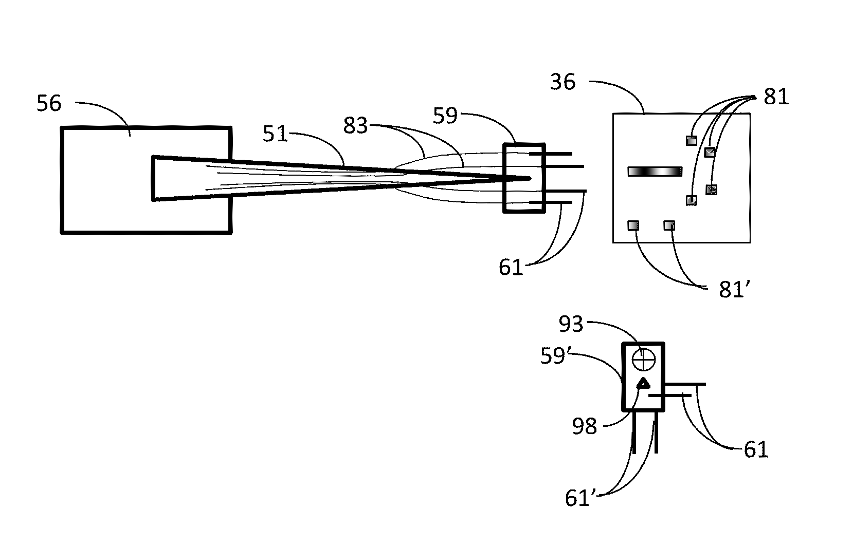
[0027] FIG. 4 illustrates an embodiment of a nanoprobe head having multiple nanoprobe tips at a fixed orientation.
DETAILED DESCRIPTION
[0028] Various features of the invention are implemented using hardware, software, or combination of hardware and software to provide parametric testing of semiconductor devices using nanoprobes. The probed devices may be in a form of microchips, die, wafer pieces, or full wafer. Generally, when the probed devices are in the form of microchips, they are de-capsulated and sometimes some layers are removed so as to expose contact targets. The contact targets are used to apply electrical test signals to the device. The various disclosed embodiments provide improved processes to make proper contact between the nanoprobes and the contact targets. The various embodiments and features are explained with reference to the tester arrangement illustrated in FIG. 1. The processes described may utilize various steps that are automated, semi-automated (i.e., require some user input to execute) or manual (i.e., executed according to directions by a user).
[0029] With reference to FIG. 1 and in accordance with an embodiment of the invention, a scanning electron microscope (SEM) nanoprobe 10 includes an electron gun 12, a set of scan coils 14, 16, 18, 20, a sample stage 22, and a set of nanoprobes 24, 26, 28, 30 that are housed inside a vacuum chamber 32. The electron gun 12 includes an anode and cathode (not shown) to which an accelerating voltage is applied to create a relatively large potential difference that extracts an emission current from the cathode and, thereby, generates a primary electron beam 25 by either field emission or thermionic emission. Located inside the vacuum chamber 32 of the SEM nanoprobe 10 is a column 33 that features various condenser lenses, objective lenses, and apertures, which collectively operate as electron optics that focus and collimate the primary electron beam 25 in the travel path from the electron gun 12 to the sample stage 22. The scan coils 14, 16, 18, 20 are also located inside the vacuum chamber 32. The sample stage 22 is movable under the management of a stage controller 34 to situate different regions of interest on a sample 36 within the field of view of the primary electron beam 25. The sample 36 may be a die carrying an integrated circuit, which has been prepared for electrical probing in the SEM nanoprobe 10 to perform root cause failure analysis. Alternatively, the sample 36 may be a wafer carrying multiple product chips.
[0030] Although described herein in relation to the use of a primary electron beam 25, a person having ordinary skill in the art will appreciate that the embodiments of the invention may also apply to the use of a focused ion beam containing positive ions, or another type of focused charged particle beam, in conjunction with nanoprobing. A person having ordinary skill in the art will understand the modifications to the SEM nanoprobe 10 required to convert the tool for use with other types of charged particles, such as positive ions for which the ion beam controls would be electro-static and not magnetic. Moreover, device 10 may include both an SEM and an ion beam column, such as, e.g., a focused ion beam, a plasma ion beam, etc. Alternatively, the SEM column may be inside vacuum chamber 32, while the ion beam column may reside in an adjacent vacuum chamber.
[0031] The scan coils 14, 16, 18, 20 are disposed within the column 33 between the electron gun 12 and the sample stage 22. The scan coils 14, 16, 18, 20 are energized to scan the primary electron beam 25 in two dimensions across a region of interest on the surface of the sample 36. To that end, one set of scan coils 14, 16 is configured to deflect the primary electron beam 25 relative to the surface of the sample 36 in a first direction and the other set of coils 18, 20 is configured to deflect the primary electron beam 25 relative to the surface of the sample 36 in a second direction orthogonal to the first direction.
[0032] When irradiated by the primary electron beam 25, secondary electrons 35 are emitted from the sample 36. The secondary electrons 35 are produced by interactions of the primary electron beam 25 with atoms at, or near, the surface of the sample 36. The secondary electrons 35 are collected by a secondary electron detector 38 located inside the vacuum chamber 32. Typically, the secondary electron detector 38 includes a phosphor or scintillator that converts the collected secondary electrons 35 into flashes of light and a photomultiplier that converts these flashes of light into amplified electrical signals. The secondary electron detector 38 is positively biased to attract the secondary electrons 35.
[0033] The amplified electrical signal output from the secondary electron detector 38 is converted by an image display control unit 40 to video signals, which are supplied to a video display unit 42 for display as a secondary electron image of a field of view on the sample 36. The secondary electron image contains a two-dimensional intensity distribution or map of the secondary electron emission prompted by the interaction of the primary electron beam 25 with the surface of the sample 36. The intensity of the individual pixels in the secondary electron image displayed on the video display unit 42 depends on the number of secondary electrons 35 from the corresponding location on the sample 36 that reach the secondary electron detector 38. Alternatively, secondary electron image from the sample 36 may be digitized into discrete pixels before display on the video display unit 42 and saved in a digital format in the storage 70 of the controller 64. The number of secondary electrons 35 emitted from any point on the sample 36 depends on the type of material exposed to the primary electron beam 25 and to the topography of the sample.
[0034] The travel path of the primary electron beam 25 passes through the scan coils 14, 16, 18, 20 in the column 33 of the SEM nanoprobe 10. The scan coils 14, 16, 18, 20 cooperate to deflect the primary electron beam 25 in the x- and y-axes so that, downstream from the scan coils 14, 16, 18, 20, the primary electron beam 25 scans in a pre-set pattern relative to a surface area on the sample 36. An electron beam control unit 44 is configured to monitor and control deflection of the primary electron beam 25 by the scan coils 14, 16, 18, 20 with applied excitation voltages. To that end, the electron beam control unit 44 is configured to generate the preset pattern by enabling raster scans of the primary electron beam 25, vector scans of the primary electron beam 25, beam dwell or sweep timings, and beam blanking.
[0035] The SEM nanoprobe 10 includes various control modules that are used to control and manage the primary electron beam 25, as well as operation of the sample stage 22, secondary electron imaging, and electrical probing. For raster scans, the scan coils 14, 16, 18, 20 may be supplied with a two-dimensional scan signal having an amplitude corresponding to the final magnification from a scan signal generator circuit 46 in the electron beam control unit 44. A raster control module 48 of the electron beam control unit 44 is configured to indicate a starting corner of a raster set, a sweep rate (or a dwell and a step rate), initial and terminal positions of the raster scan lines, the spacing between successive raster scan lines, and the height of raster boxes to the scan signal generator circuit 46. A vector control module 50 of the electron beam control unit 44 is configured to indicate a vector start point, a vector direction, a vector terminal point, and a sweep rate for vector scan lines of the primary electron beam 25 to the scan signal generator circuit 46.
[0036] A beam blanking control module 52 of the electron beam control unit 44 is configured to set start and stop locations for blanking of the primary electron beam 25 when moved across the sample 36 in either raster scans or vector scans. The beam blanking control module 52 may apply a voltage to a set of deflection plates 53, 55 to deflect the primary electron beam 25 laterally onto a downstream aperture stop 57 in the column 33, thereby blanking the beam 25 so that the primary electrons are not incident on the sample 36. The primary electron beam 25 is restored by removing the voltage from the deflection plates 53, 55 so that the primary electron beam 25 again permitted to travel to the sample 38 through an opening in the aperture stop 57. When the beam blanking control module 52 is operated to blank the primary electron beam 25, the secondary electron emission from the sample 36 ceases as the primary electron beam 25 is blocked from traveling to the sample 36.
[0037] In a raster scanning mode, the movement of the primary electron beam 25 across the sample 36 is divided into a sequence of horizontal strips known as scan lines. Each of the scan lines is implemented by causing the scan signal generator circuit 46 in the electron beam control unit 44 to operate the scan coils 14, 16, 18, 20 to deflect the primary electron beam 25 at fixed increments (or as a continuous sweep) along a linear path parallel to one axis from a start point to an end point. The primary electron beam 25 is permitted to dwell for a fixed dwell time at each intervening point between the start and end points. At the end point of each scan line, the position of the primary electron beam 25 is incrementally advanced along a second axis orthogonal to the first axis. The primary electron beam 25 may return to the start point of the first axis to initiate the net successive scan line, or the primary electron beam 25 may be deflected in the reverse direction from the end point back toward the start point. This process continues until all raster scan lines have been traced on the sample 36 and the primary electron beam 25 has dwelled at all points in each scan line.
[0038] The image display control unit 40 of the SEM nanoprobe 10 manages the operation of the video display unit 42. The secondary electron image 94 (FIG. 3) is periodically refreshed on the video display unit 42. The image display control unit 40 closely synchronizes the secondary electron image 94 displayed on the video display unit 42, or stored in a display buffer 54 and periodically forwarded to the video display unit 42, with the deflections of the primary electron beam 25 caused by the electron beam control unit 44 and scan coils 14, 16, 18, 20. The resulting secondary electron image 94 on the video display unit 42 is therefore a distribution map of the intensity of secondary electrons 35 being emitted from the scanned area on the sample 36 and is intimately linked thereto.
[0039] The image display control unit 40 has the capability to superimpose a CAD layout on the secondary electron image 94 on the video display unit 42 and capture such operator-defined information for control of the electron beam by the electron beam control unit 44. The image display control unit 40 includes a compensation control for SEM magnification to scale images for the electron beam field of view and to scale masks, zones, or CAD layout. Using the secondary electron image 94, the nanoprobes 24, 26, 28, 30 are maneuvered by motorized nanomanipulators 56, 58, 60, 62 to position the tips of the nanoprobes 24, 26, 28, 30 in direct contact with conductive features on the sample 36. During this positioning process, the location of the contacts on the sample 36 and, optionally, the real-time position of the probes 24, 26, 28, 30 are monitored using the secondary electron image 94. When the tips of the probes 24, 26, 28, 30 are properly positioned, electrical test signals are directed from the probes 24, 26, 28, to the conductive features on the sample 36. As appreciated by a person having ordinary skill in the art, the exact number of probes 24, 26, 28, 30 associated with the SEM nanoprobe 10 may differ from the representative number depicted in FIG. 1, and may range from one (1) to eight (8), or even more than eight, according to the type of electrical test measurement.
[0040] The operation of the SEM nanoprobe 10 is coordinated and controlled by a controller 64, which is electrically coupled with stage controller 34, image display control unit 40, and electron beam control unit 44. The controller 64 includes a processor 66 and a memory 68 coupled with the processor 66. Processor 66 may represent one or more individual processors (e.g., microprocessors), and memory 68 may represent the random access memory (RAM) devices comprising the main storage of controller 64, as well as any supplemental levels of memory, e.g., cache memories, non-volatile or backup memories (e.g., programmable or flash memories), read-only memories, etc. In addition, memory 68 may be considered to include memory storage physically located elsewhere in controller 64, e.g., any cache memory in the processor 66, as well as any storage capacity used as a virtual memory, e.g., as stored on a mass storage device 70. The mass storage device 70 may contain a cache or other data storage, which may include one or more databases 72. The databases 72 may, for example, contain CAD navigation data and CAD layout data for use in practicing embodiments of the invention.
[0041] Controller 64 also typically receives a number of inputs and outputs for communicating information externally. For interfacing with a user or operator, controller 64 typically includes a graphical user interface 74 with one or more input devices, such as a keyboard, a mouse, a trackball, a joystick, a touchpad, a keypad, a stylus, and/or a microphone, among others, as well a display, such as a CRT monitor, an LCD display panel, and/or a speaker, among others, or other type of output device, such as a printer. The interface to controller 64 may also be through an external terminal connected directly or remotely to controller 64, or through another computer communicating with controller 64 via a network 76, modem, or other type of recognized communications device. Controller 64 communicates on the network 76 through a network interface 78.
[0042] Controller 64 operates under the control of an operating system 80 and executes or otherwise relies upon various computer software applications, components, programs, objects, modules, data structures, etc. In general, the routines executed to implement the embodiments of the invention, whether implemented as part of an operating system or a specific application, component, program, object, module or sequence of instructions will be referred to herein as "computer program code", or simply "program code". The computer program code typically comprises one or more instructions that are resident at various times in various memory and storage devices in a computer, and that, when read and executed by one or more processors in a computer, causes that computer to perform the steps necessary to execute steps or elements embodying the various aspects of the invention.
[0043] The SEM nanoprobe 10 may provide a user with the ability to program the controller 64 with instructions and settings for the various embodiments used to test various regions of the device. For example, the user may supply instructions for selecting the contact targets for the nanoprobes via the user interface 74. Alternatively, the instructions for the selection of targets and selection of test protocols may be received remotely, such as from another computer that is operatively coupled to controller 64 through network 76, for example.
[0044] FIG. 2 is a sketch illustrating a plurality of nanoprobe tips 24, 26, 28 and 30 contacting various targets on device 36. The device structure 82 may be, for example, a field effect transistor or a memory cell containing several field effect transistors, etc. The tips of the probes 24, 26, 28, 30 are placed in contact with the terminals or contact targets 84, 86, 88, 90 for electrical characterization of the device structure 82 of the device under testing (DUT). The contact targets may actually be smaller than the probe tips themselves. FIG. 3 illustrates an SEM image of a region of interest ROI of the device 36, showing some of the contacts and some of the nanoprobe tips. Also shown in FIG. 3 is a cursor 100 that may be used by the user as will be described in more details below. For clarity, not illustrated in FIG. 3 is the ability to superimpose a CAD design image corresponding to the ROI.
[0045] According to embodiments of the invention, a database 148 may be interrogated by the processor 66 via network 76. Alternatively, appropriate data from the database is sent to or downloaded onto the memory 68. The data in database 148 may take the form of CAD design data, a Netlist, or both. Conversely, the CAD design data and Netlist may be stored on two different databases that may be connected independently to network 76. CAD design data describes the planned geometrical shape of various layers on the integrated circuit, while Netlist describes the connectivity of an electronic design, that is, a single Netlist is a list of all the component terminals that should be electrically connected together for the circuit to work. So, while the CAD design data provides visual image that may be compared to and registered/aligned to the SEM image, the Netlist provides electrical connectivity data relating to various elements shown in the SEM image. Thus, for example, a Netlist may indicate whether and when contact 84 should be electrically connected to contact 86. Such information is not directly provided by the CAD design data or the SEM image. Knowledge of this connectivity helps in determining which contact targets are appropriate for performing which tests. For example, if the Netlist indicates that contacts 84 and 86 should be electrically connected, which is not visible to the SEM since the connection may be in lower, obscured, layers of the device, then one nanoprobe may apply potential to contact 84 and another nanoprobe can be used to check the potential on contact 86, to verify that they are indeed electrically connected.
[0046] According to another embodiment, the SEM is used to generate a voltage contrast image, and the voltage contrast image is used to identify the targets. Specifically, according to this embodiment an electrical potential is applied to the wafer. For example, the electrical potential may be applied to the wafer using the wafer support, wherein the wafer support includes an electrode to apply the electrical potential to the wafer. Of course, the electrical potential can be 0V, i.e., ground potential. According to another example, one or more of the nanoprobe tips may contact conductive elements within the wafer and apply electrical potential. Then the SEM column is used to scan an electron beam over the ROI and collect secondary electrons emanating from the ROI. The amount of secondary electrons would differ from regions that are at the applied electrical potential and those that are insulated from the electrical potential. Thus, a voltage contrast image is generated from the secondary electrons, wherein regions that are at the applied potential appear at different intensity than regions that are insulated from the electrical potential. Such an embodiment is referred to herein as active voltage contrast. Embodiments wherein the voltage applied by the nanoprobes tips varies is referred to herein as dynamic voltage contrast. The voltage contrast image may then be used to identify targets for nanoprobe tips. According to another embodiment, the voltage contrast image may be superimposed on the SEM topography image or on the CAD image to better identify suitable targets. Additionally, the Netlist can also be used in conjunction with the voltage contrast image to identify suitable targets.
[0047] According to one embodiment, a static voltage contrast image is obtained by scanning the electron beam over the ROI while applying voltage potential to the wafer using the wafer support. Then an active voltage contrast or dynamic voltage contrast image is obtained, by scanning the ROI while applying voltage to the wafer using the nanoprobes. The active or dynamic image is then compared to the static voltage contrast image to determine location and types of defects in the DUT.
[0048] According to one embodiment, an automatic target acquisition is achieved by the processor 66. According to one example, the processor executes a process wherein the processor operates the SEM to generate an SEM image of an ROI. Then the processor compares the SEM image to CAD design data to identify the location of the ROI with respect to the remainder of the DUT. Once the processor identifies the location ROI, it identifies elements within the ROI, e.g., contacts 84 and 86 and line 92. The processor then interrogates the Netlist to determine which elements within the ROI should be contacted by a nanoprobe to perform electrical tests. Once the processor determines which elements should be contacted, the processor assigns a nanoprobe to each of the elements. Incidentally, the assignment of nanoprobe may also be performed by a user operating the cursor 100 and clicking on different elements and probers. Once the nanoprobes have been assigned to their respective elements, the processor 66 calculate motion vector for each nanoprobe and check to ensure that the motion according to the motion vectors does not result in collision of the nanoprobes. When no collision is detected, the processor 66 issues a motion vector to each nanoprobe to move its tip towards the assigned element. Each of the above steps may be performed automatically, semi-automatically (i.e., with some input from a user) or manually.
[0049] According to further embodiments, once the processor obtains the CAD design data for the ROI, the processor select a parametric test from a library of parametric tests, depending on the design indicated by the CAD design data. For example, the processor 66 may select a different parametric test depending on whether the CAD design data indicates that the ROI encompasses an SRAM, a diode, a memory cell, etc. Additionally, depending on the CAD design data, the processor may select the number of nanoprobes to be used in the parametric test. Alternatively, the test is selected according to information received from the Netlist.
[0050] As indicated previously, there may be times when the sample needs to be transferred to another device to further investigate a particular element within a sample, or to prepare the sample for further investigation. However, in today's technology the elements are of nano-size and are very difficult to find, even using the most advanced particle microscopes. Therefore, according to one embodiment, when the SEM acquires a target of interest, and it is determined that the sample may need to be investigated further, the processor follows the following process. The processor determines a safe region within the ROI. The safe region may be determined by a user indicating the location, e.g., using the cursor 100, or by the processor performing the determination automatically, semi-automatically, or in conjunction with interrogation of the CAD design data. A safe location is defined as a location that is not part of the electrical circuitry. For example, it may be an insulation area, such as area 105 shown in FIG. 3. The processor then send motion vector to one of the nanoprobes to move towards the safe area. Once the nanoprobe arrives at the safe area, the processor issues instructions to the nanoprobe to scratch a mark in the same area. For that purpose, according to one embodiment, one of the nanoprobe is fitted with a specialty tip, e.g., a hardened tip made of, e.g, diamond, silicon-carbide (SiC), zirconia, Al2O3 or other hard material, and it is the only nanoprobe used for scratching the samples. Thus, for example, apparatus 10 may include several nanoprobes having conductive tips, e.g., made of tungsten, while also include one or more nanoprobed having hardened tips that may be made of an insulator and which are not used for parametric testing. Alternatively, one of the conductive tip nanoprobe may be used for scratching, although it may require earlier replacement due to dulling or bending of the tip. The scratch mark then may be used by other particle or optical microscope to more readily find and identify the ROI and/or the target within the ROI.
[0051] From the above described process, an embodiment of the invention may include a method for investigating a sample, which includes imaging a region of interest within the sample, identifying a safe location for marking the ROI, using a nanoprobe to scratch a mark in the safe location, and transferring the sample to another station, e.g., a forced ion beam, and acquiring the ROI at the next station by searching for the scratch using a microscope, e.g., an optical or a particle beam microscope. If the second station does not include an imaging tool, but is used to deprocesses an area, e.g., remove layers from the area, the safe marking area would then need to be outside of the area that gets deprocessed.
[0052] The probing of a DUT may include a step of marking further regions of interest using a hardened probe. According to this embodiment, a combination of scanning electron microscope (SEM) and nanoprobes is used to probe the DUT by following the steps of: obtaining an SEM image of a region of interest (ROI) in the DUT; obtaining a CAD design image of the ROI; registering the CAD design image with the SEM image to identify contact targets; obtaining an electrical design corresponding to the contact targets and using the electrical design to determine which of the contact targets should be selected as test target; navigating nanoprobes to land a nanorpobe on each of the test targets and form electrical contact between the nanoprobe and the respective test target; and using a nanoprobe having a hardened tip to make a mark on any ROI requiring further investigation. The electrical design may be in the form of a Netlist.
[0053] According to another embodiment, the following method is performed to overcome natural drift in the system e.g., drift of the sample or parts the system due to thermal variations. In one example, once the type of test to be performed is determined, the time period required to perform the entire test is determined. The time period is then compared to a threshold period. The threshold period may be calculated according to expected or potential drift time. For example, depending on the material of the sample, it may be determined that within five seconds the drift may be sufficiently large so as to strain the tip contacting the contact element or cause the tip to slide away from the contact element. Thus, the threshold period may be set to four or five seconds. If it is determined that the test period is larger than the drift period, the test is broken into several sub-tests, each requiring a sub-period of the total test period. For example, if it was determined that the entire test would take 30 seconds to complete, the test may be broken into six sub-tests, each requiring five seconds to complete. Then between each sub-test, the tips are raised from their contact element, the ROI imaged, the alignment of the nanoprobes to their respective landing targets is corrected if a drift was detected, and the tips are re-landed on their respective contact elements for the next sub-test.
[0054] In the above method, it may be that each sub-test requires a different number of nanoprobes, since each sub-test may test different elements within the ROI. In such a case, for each sub-test the method proceed by identifying the number of contact elements participating in such sub-test. Then the method proceeds by assigning nanoprobes to those contact elements. Then, for each sub-test, only a subset of the nanoprobes are landed on the assigned elements, as required for that particular subtest. At the end of each subtest, the landed nanoprobes are lifted off the contact elements and the next subset is landed on the next set of contact elements to perform the next sub-test.
[0055] Another embodiment of the invention helps in shortening the time to target acquisition by a-priory knowledge of the expected geometrical arrangement of the contact elements for the nanoprobes. For example, with respect to the illustration of FIG. 2, the design structure 82 may be repeating many times throughout the sample. It may also be repeated in other samples of the same or similar chip design. Therefore, according to this embodiment, the design is stored in the memory storage, e.g., storage 70 or database 148, together with associated geometrical shape of the contact elements and motion vectors for the assigned nanoprobes. For example, the image of element 82 may be stored together with a geometrical shape mimicking a number 6 as appearing on a die, i.e., two parallel rows of three dots each, and associated motion vectors, each with its assigned nanoprobe. Then, when the specific shape is recognized in the field of view of the SEM, the pattern may be immediately recognized and the motion vectors sent to the assigned nanoprobes.
[0056] On the other hand, FIG. 4 illustrates another embodiment specifically tailored for testing repetitive pattern arrangements. In FIG. 4, the nanoprobe comprises a micromanipulator, such as, e.g., manipulator 56. A probe arm 51 is attached at one end to the manipulator 56, such that the manipulator can move the arm 51 according to the motion vectors. A probe head 59 is attached at the other end of the arm 51, and is sometimes referred to herein as nanoprobe card. The probe head 59 has a plurality of probe tips 61 that are fixedly attached to the probe head 59. The probe tips 61 are attached to the probe head 59 at a single specific orientation such as to correspond to a specific geometry of contact elements. In the example of FIG. 4, the four probe tips 61 are attached to the probe head 59 at a fixed orientation that corresponds to the arrangement of contact elements 81 of DUT 36. Since the probe tips 61 are fixedly attached to the probe head 59 in one single orientation, this particular probe head may be used only for tests that utilize contact elements 81. Note, however, that other standard nanoprobes in the system can be used to contact other contact elements if needed. However, for any device having contact elements arranged as element 81, this particular probe head can be used. This arrangement has the advantage of being able to land four nanoprobes simultaneously using a single actuator 56.
[0057] In the embodiment of FIG. 4, four separate leads 83 are provided, one for each of the probe tips 61. In this manner, each probe tip can deliver different current or signal to its contact element separately. Of course, if all of the contact points are to be energized with the same current or test signal, one lead 83 can be used to deliver power to the four tips 61.
[0058] Also illustrated in FIG. 4 is the provision of replacement probe head 59'. Visible in FIG. 4 is the provision of quick disconnect coupler 98 on the probe head. A corresponding disconnect coupler is provided on the 52, but is not visible in the illustration of FIG. 4. The provision of disconnect coupler enables replacement of the probe heads for testing different targets or for running different tests.
[0059] As shown in this example, replacement probe head 59' has two probe tips designed to contact two of the lower four contact elements 81 and two probe tips 61' oriented to land on contact elements 81'. Thus, according to one embodiment, the probe heads are removable from arm 51 and exchangeable with other probe heads. Also, according to one embodiment, each DUT has a set of probe heads 59 fabricated specifically for test elements to be found on the particular DUT. Thus, when a DUT is selected for testing, the set of probe heads assigned to the particular DUT is determined and mounted on respective probe arms.
[0060] According to another embodiment, also illustrated in FIG. 4, an alignment target is provided on the top surface of the probe head. This is shown on probe head 59' only, but can be provided on any probe head. The alignment target is configured to be visible by an SEM or other particle microscope. This may be done using varying topography or material. For example, the probe head 59 may be made of ceramic material, while the target 93 may be a deposited or embedded conductor, such as gold. When the manipulator 56 moves the arm to align the probe tips to land on their target, the SEM may be used to image the probe head and use the alignment target to ensure that all of the probe tips will indeed land on their contact element.
[0061] In the embodiments described above, after the probe tips are landed on their respective targets, the controller sends test signals to each of the probers. The test signals may be a simple positive, negative, or ground potential, or may actually be a varying analog or digital signal, or a combination of these. As those signals are transmitted to the probe tips, regions and elements in the circuit that have conductive path to the test signals at any of the probe tips, will assume that electrical potential. It can be said that the element or region is at the test signal potential. During that time, the SEM column is operated to scan an electron beam over the ROI and collect secondary electrons emanating from the ROI. The secondary electrons correlate to the potential of each region or element within the ROI, and can be used to generate a probe voltage contrast image. This probe voltage contrast image can be compared to a voltage contrast image generated before the tips were landed on the targets, to thereby investigate interconnect defects in the electrical circuit.
[0062] The terminology used herein is for the purpose of describing particular embodiments only and is not intended to be limiting of the invention. As used herein, the singular forms "a", "an" and "the" are intended to include the plural forms as well, unless the context clearly indicates otherwise. It will be further understood that the terms "comprises" and/or "comprising," when used in this specification, specify the presence of stated features, integers, steps, operations, elements, and/or components, but do not preclude the presence or addition of one or more other features, integers, steps, operations, elements, components, and/or groups thereof. Furthermore, to the extent that the terms "includes", "having", "has", "with", or variants thereof are used in either the detailed description or the claims, such terms are intended to be inclusive in a manner similar to the term "comprising." It is also understood that features of the embodiments of the invention are not necessarily shown to scale in the drawings.
[0063] The steps described for the disclosed processes may be manual, partially automated or substantially automated. For example, manual steps may substantially rely on user input. Partially automated embodiments of the processes may automatically perform a subset of the actions and/or decisions of the process, while relying on a user input for the remainder of the actions/decisions. Automated aspects of partially automated embodiments may include process initiation, process performance, process monitoring and/or adjustment (e.g., time, power, speed, force, etc.), process termination, and/or process errors, among others. Substantially automated embodiments of the processes may substantially rely on automated robotics and/or other machinery or apparatus, and/or substantially automated computing hardware and/or software, such that, e.g., the selection of probes during process may be performed in the substantial absence of user input. This convention, where the extent of automation may substantially be inversely proportional to the amount of user input required or employed during a particular method or method component, or a particular apparatus or function thereof, is also applicable to other aspects of the methods, as well as to aspects of other methods and apparatus within the scope of the present disclosure.
[0064] The corresponding structures, materials, acts, and equivalents of all means or step plus function elements in the claims below are intended to include any structure, material, or act for performing the function in combination with other claimed elements as specifically claimed. The description of the present invention has been presented for purposes of illustration and description, but is not intended to be exhaustive or limited to the invention in the form disclosed. Many modifications and variations will be apparent to those of ordinary skill in the art without departing from the scope and spirit of the invention. The embodiment was chosen and described in order to best explain the principles of the invention and the practical application, and to enable others of ordinary skill in the art to understand the invention for various embodiments with various modifications as are suited to the particular use contemplated.
* * * * *
D00000
D00001
XML
uspto.report is an independent third-party trademark research tool that is not affiliated, endorsed, or sponsored by the United States Patent and Trademark Office (USPTO) or any other governmental organization. The information provided by uspto.report is based on publicly available data at the time of writing and is intended for informational purposes only.
While we strive to provide accurate and up-to-date information, we do not guarantee the accuracy, completeness, reliability, or suitability of the information displayed on this site. The use of this site is at your own risk. Any reliance you place on such information is therefore strictly at your own risk.
All official trademark data, including owner information, should be verified by visiting the official USPTO website at www.uspto.gov. This site is not intended to replace professional legal advice and should not be used as a substitute for consulting with a legal professional who is knowledgeable about trademark law.