Method For Fabricating Metal-oxide- Semiconductor Field-effect Transistor
LU; Ching-Sen ; et al.
U.S. patent application number 13/165854 was filed with the patent office on 2012-12-27 for method for fabricating metal-oxide- semiconductor field-effect transistor. This patent application is currently assigned to UNITED MICROELECTRONICS CORP.. Invention is credited to Tsai-Fu CHEN, Tzyy-Ming CHENG, Wen-Han HUNG, Ching-Sen LU.
| Application Number | 20120329259 13/165854 |
| Document ID | / |
| Family ID | 47362242 |
| Filed Date | 2012-12-27 |
| United States Patent Application | 20120329259 |
| Kind Code | A1 |
| LU; Ching-Sen ; et al. | December 27, 2012 |
METHOD FOR FABRICATING METAL-OXIDE- SEMICONDUCTOR FIELD-EFFECT TRANSISTOR
Abstract
A method for fabricating a metal-oxide-semiconductor field-effect transistor includes the following steps. Firstly, a substrate is provided. A gate structure, a first spacer, a second spacer and a source/drain structure are formed over the substrate. The second spacer includes an inner layer and an outer layer. Then, a thinning process is performed to reduce the thickness of the second spacer, thereby retaining the inner layer of the second spacer. After a stress film is formed on the inner layer of the second spacer and the source/drain structure, an annealing process is performed. Afterwards, the stress film is removed.
| Inventors: | LU; Ching-Sen; (Tainan City, TW) ; HUNG; Wen-Han; (Kaohsiung City, TW) ; CHEN; Tsai-Fu; (Hsinchu City, TW) ; CHENG; Tzyy-Ming; (Hsinchu City, TW) |
| Assignee: | UNITED MICROELECTRONICS
CORP. HSINCHU TW |
| Family ID: | 47362242 |
| Appl. No.: | 13/165854 |
| Filed: | June 22, 2011 |
| Current U.S. Class: | 438/586 ; 257/E21.158; 257/E21.19 |
| Current CPC Class: | H01L 29/6653 20130101; H01L 29/66545 20130101; H01L 29/7847 20130101; H01L 29/7833 20130101; H01L 29/6656 20130101 |
| Class at Publication: | 438/586 ; 257/E21.158; 257/E21.19 |
| International Class: | H01L 21/28 20060101 H01L021/28 |
Claims
1. A method for fabricating a metal-oxide-semiconductor field-effect transistor, the method comprising steps of: providing a substrate, wherein a gate structure, a first spacer, a second spacer and a source/drain structure are formed over the substrate, and the second spacer comprises an inner layer and an outer layer; thinning the second spacer, thereby retaining the inner layer of the pacer; forming a stress film on the inner layer of the second spacer and the source/drain structure, and then performing an annealing process; and removing the stress film.
2. The method according to claim 1, wherein the substrate is a silicon substrate, and the gate structure comprises a gate dielectric layer, a barrier metal layer, a polysilicon dummy gate and a hard mask layer, wherein the first spacer is a silicon nitride layer or a multi-layered structure including a silicon dioxide layer and a silicon nitride layer, the inner layer of the second spacer is made of silicon dioxide, and the outer layer of the second spacer is made of silicon nitride.
3. The method according to claim 2, wherein the gate dielectric layer comprises an interlayer and a high-K dielectric layer, and the hard mask layer comprises a silicon nitride layer and a silicon dioxide layer, wherein the high-K dielectric layer is made of hafnium dioxide, the interlayer is made of silicon dioxide, and the barrier metal layer is made of titanium nitride.
4. The method according to claim 2, wherein the source/drain structure is formed in the substrate by performing an ion-implanting process to transform a crystal phase of the silicon substrate into an amorphous phase.
5. The method according to claim 2, wherein the step of thinning the second spacer is performed by using a hot phosphoric acid solution to etch the second spacer, so that the outer layer of the second spacer is removed but the inner layer of the second spacer is retained.
6. The method according to claim 2, wherein after the stress film is removed, the method further comprises steps of: forming a contact etch stop layer and an interlayer dielectric layer over the substrate; performing a chemical mechanical polishing process to remove a portion of the contact etch stop layer, a portion of the interlayer dielectric layer and the hard mask layer, thereby exposing the polysilicon dummy gate; removing the exposed polysilicon dummy gate, thereby creating a trench; and filling a metal gate structure into the trench.
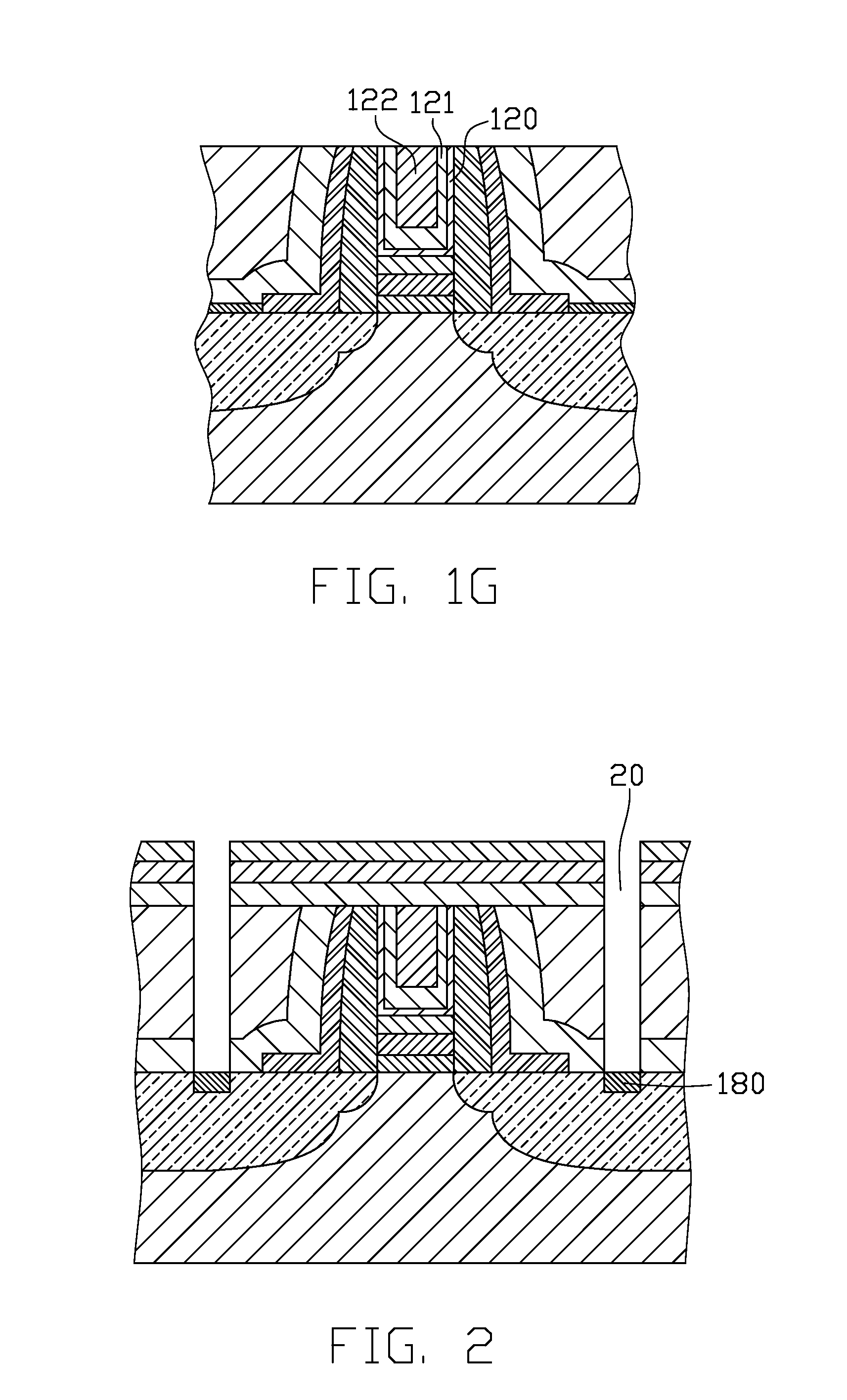
7. The method according to claim 6, wherein the step of filling a metal gate structure is performed by sequentially filling an etch stop layer, a work function metal layer and a metal gate into the trench.
8. The method according to claim 7, wherein the etch stop layer is made of made of titanium nitride (TiN), the work function metal layer is made of titanium nitride (TiN) or titanium aluminum (TiAl), and the metal gate is made of aluminum (Al).
9. The method according to claim 1, wherein after the stress film is removed, the method further comprises a step of: forming a salicide layer on the source/drain structure.
10. The method according to claim 1, wherein the stress film is a silicon nitride film or a composite film including a buffer oxide film and a silicon nitride film.
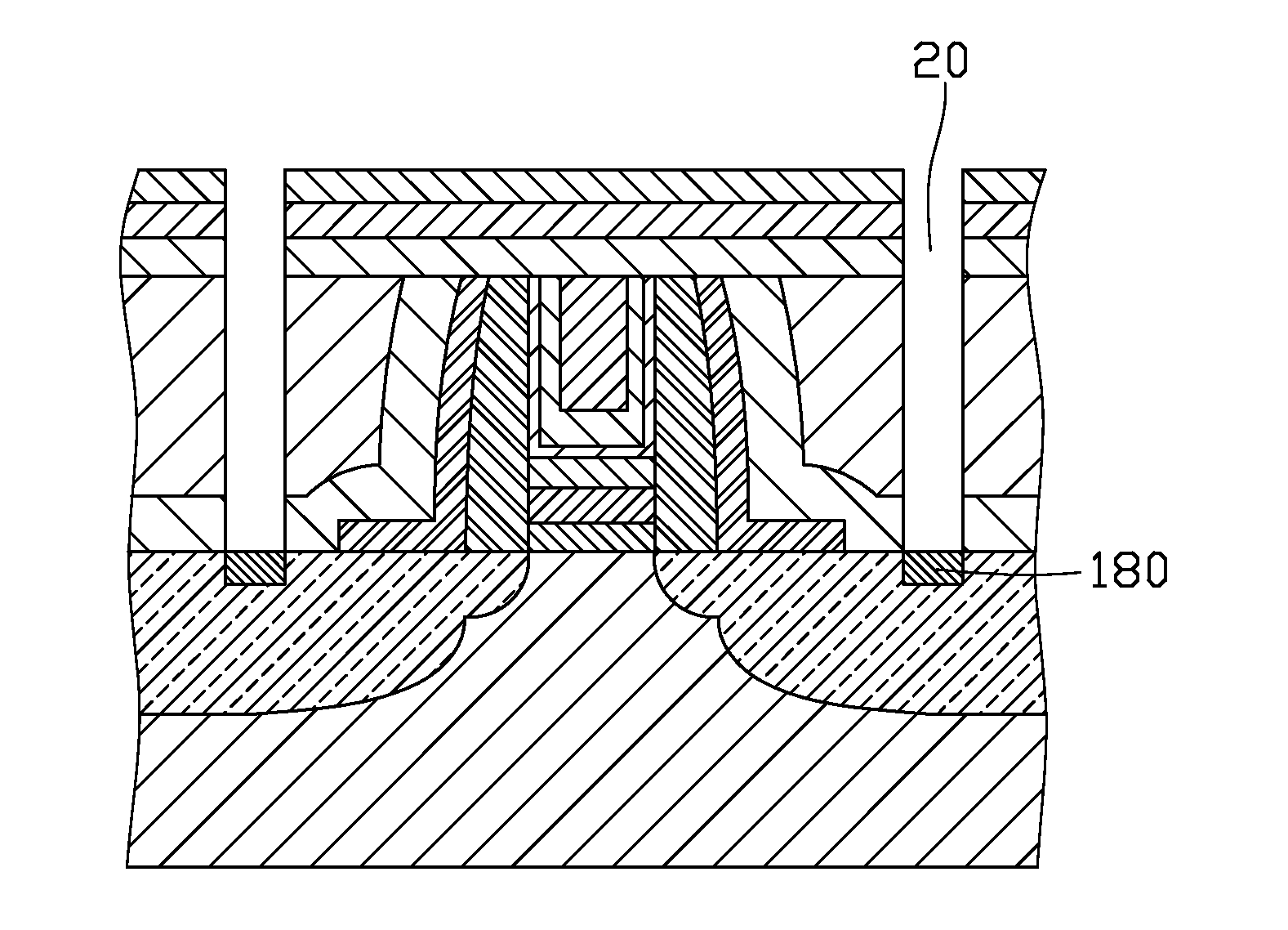
11. The method according to claim 1, wherein the metal-oxide-semiconductor field-effect transistor is a p-channel metal-oxide-semiconductor field-effect transistor, and the stress film is a compressive stress film.
12. The method according to claim 1, wherein the metal-oxide-semiconductor field-effect transistor is an n-channel metal-oxide-semiconductor field-effect transistor, and the stress film is a tensile stress film.
13. The method according to claim 1, wherein the step of removing the stress film is performed by a wet etching process.
14. The method according to claim 1, further comprising steps of: forming a contact hole over the source/drain structure, thereby exposing a surface of the source/drain structure; and forming a salicide layer on the exposed surface of the source/drain structure.
Description
FIELD OF THE INVENTION
[0001] The present invention relates to a method for fabricating a semiconductor device, and more particularly to a method for fabricating a metal-oxide-semiconductor field-effect transistor.
BACKGROUND OF THE INVENTION
[0002] Because the length of the gate can not be limitlessly reduced any more and new materials have not been proved to be used in a metal-oxide-semiconductor field-effect transistor (MOSFET), adjusting mobility has become an important role to improve the performance of the integrated circuit. For example, the lattice strain of the channel is widely applied to increase mobility during the process of fabricating the MOSFET. For example, the hole mobility of the silicon with the lattice strain can be 4 times as many as the hole mobility of the silicon without the lattice strain, and the electron mobility with the lattice strain can be 1.8 times as many as the electron mobility of the silicon without the lattice strain.
[0003] Consequently, a tensile stress can be applied to an n-channel of an n-channel metal-oxide-semiconductor field-effect transistor (NMOS) by changing the structure of the transistor, or a compressive stress can be applied to a p-channel of a p-channel metal-oxide-semiconductor field-effect transistor (PMOS) by changing the structure of the transistor. Based on these characteristics, a stress memorization technique (SMT) is developed. However, the performance of the semiconductor device fabricating by the current stress memorization technique is still unsatisfied. Therefore, there is a need of providing an improved method for fabricating a metal-oxide-semiconductor field-effect transistor.
SUMMARY OF THE INVENTION
[0004] In accordance with an aspect, the present invention provides a method for fabricating a metal-oxide-semiconductor field-effect transistor. The method includes the following steps. Firstly, a substrate is provided. A gate structure, a first spacer, a second spacer and a source/drain structure are formed over the substrate. The second spacer includes an inner layer and an outer layer. Then, a thinning process is performed to reduce the thickness of the second spacer, thereby retaining the inner layer of the second spacer. After a stress film is formed on the inner layer of the second spacer and the source/drain structure, an annealing process is performed. Afterwards, the stress film is removed.
[0005] In an embodiment, the substrate is a silicon substrate. The gate structure includes a gate dielectric layer, a barrier metal layer, a polysilicon dummy gate and a hard mask layer. The first spacer is a silicon nitride layer or a multi-layered structure including a silicon dioxide layer and a silicon nitride layer. The inner layer of the second spacer is made of silicon dioxide. The outer layer of the second spacer is made of silicon nitride.
[0006] In an embodiment, the gate dielectric layer includes an interlayer and a high-K dielectric layer. The high-K dielectric layer is made of hafnium dioxide. The interlayer is made of silicon dioxide. The barrier metal layer is made of titanium nitride. The hard mask layer comprises a silicon nitride layer and a silicon dioxide layer.
[0007] In an embodiment, the source/drain structure is formed in the substrate by performing an ion-implanting process to transform a crystal phase of the silicon substrate into an amorphous phase.
[0008] In an embodiment, the step of thinning the second spacer is performed by using a hot phosphoric acid solution to wet etch the second spacer, so that the outer layer of the second spacer is removed but the inner layer of the second spacer is retained.
[0009] In an embodiment, after the stress film is removed, the method further includes steps of forming a contact etch stop layer and an interlayer dielectric layer over the substrate, performing a chemical mechanical polishing process to remove a portion of the contact etch stop layer, a portion of the interlayer dielectric layer and the hard mask layer to expose the polysilicon dummy gate, removing the exposed polysilicon dummy gate to create a trench, and filling a metal gate structure into the trench.
[0010] In an embodiment, the step of filling a metal gate structure is performed by sequentially filling an etch stop layer, a work function metal layer and a metal gate into the trench.
[0011] In an embodiment, the etch stop layer is made of made of titanium nitride (TiN), the work function metal layer is made of titanium nitride (TiN) or titanium aluminum (TiAl), and the metal gate is made of aluminum (Al).
[0012] In an embodiment, after the stress film is removed, the method further includes a step of forming a salicide layer on the source/drain structure.
[0013] In an embodiment, the stress film is a silicon nitride film or a composite film including a buffer oxide film and a silicon nitride film.
[0014] In an embodiment, the metal-oxide-semiconductor field-effect transistor is a p-channel metal-oxide-semiconductor field-effect transistor, and the stress film is a compressive stress film.
[0015] In an embodiment, the metal-oxide-semiconductor field-effect transistor is an n-channel metal-oxide-semiconductor field-effect transistor, and the stress film is a tensile stress film.
[0016] In an embodiment, the step of removing the stress film is performed by a wet etching process.
[0017] In an embodiment, the method further includes steps of forming a contact hole over the source/drain structure to expose a surface of the source/drain structure, and forming a salicide layer on the exposed surface of the source/drain structure.
BRIEF DESCRIPTION OF THE DRAWINGS
[0018] The above objects and advantages of the present invention will become more readily apparent to those ordinarily skilled in the art after reviewing the following detailed description and accompanying drawings, in which:
[0019] FIGS. 1A.about.1G are schematic cross-sectional views illustrating a method for fabricating a metal-oxide-semiconductor field-effect transistor according to an embodiment of the present invention; and
[0020] FIG. 2 is a schematic cross-sectional view illustrating a metal-oxide-semiconductor field-effect transistor according to another embodiment of the present invention.
DETAILED DESCRIPTION OF PREFERRED EMBODIMENTS
[0021] The present invention will now be described more specifically with reference to the following embodiments. It is to be noted that the following descriptions of preferred embodiments of this invention are presented herein for purpose of illustration and description only. It is not intended to be exhaustive or to be limited to the precise form disclosed.
[0022] For improving the stress memorization technique, the present invention provides a method for fabricating a metal-oxide-semiconductor field-effect transistor. FIGS. 1A.about.1G are schematic cross-sectional views illustrating a method for fabricating a metal-oxide-semiconductor field-effect transistor according to an embodiment of the present invention.
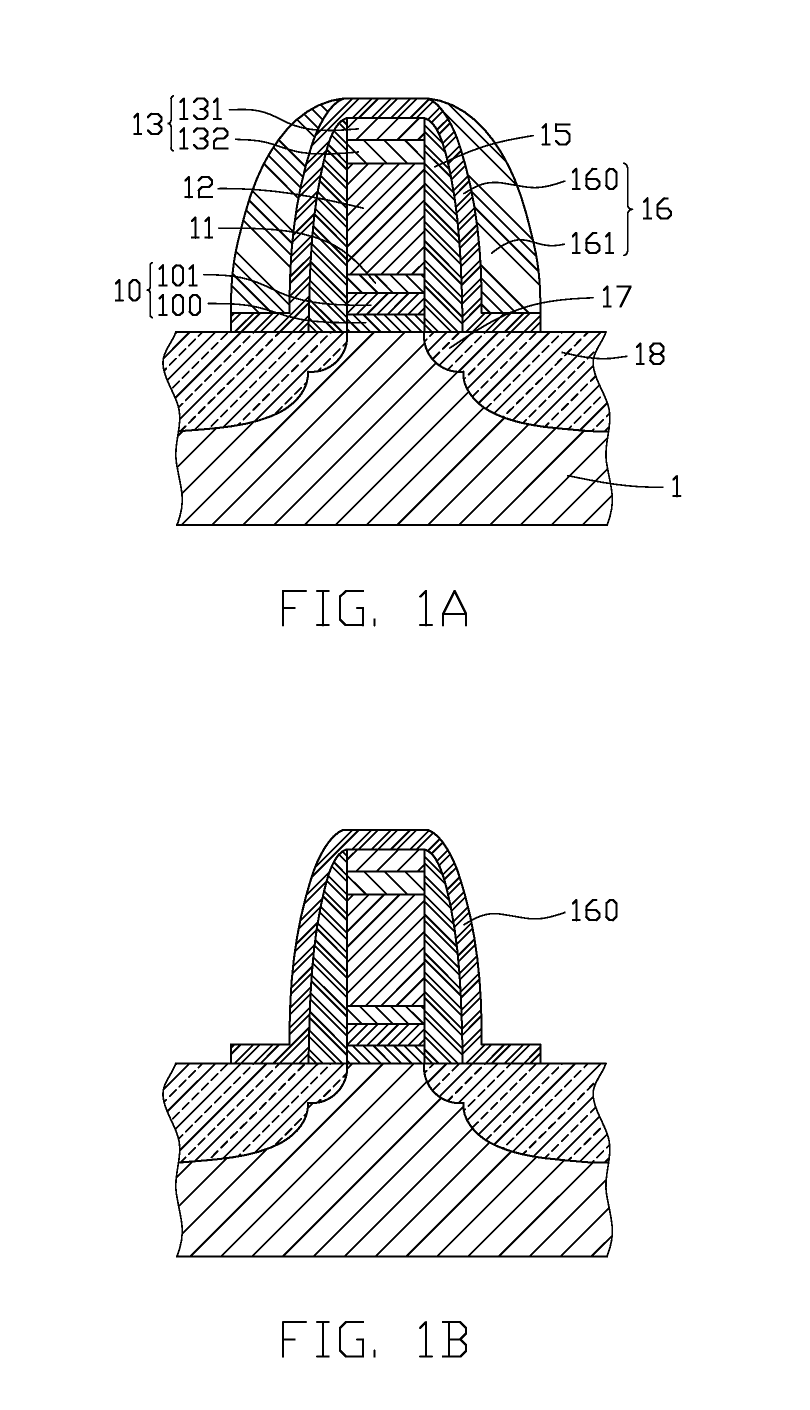
[0023] Firstly, a silicon substrate 1 is provided. After a front-end processes for producing a metal-oxide-semiconductor field-effect transistor is performed, the resulting structure is shown in FIG. 1A. A gate structure including a gate dielectric layer 10, a barrier metal layer 11, a polysilicon dummy gate 12 and a hard mask layer 13 is formed over the silicon substrate 1. The gate dielectric layer 10 is a multi-layered structure including an interfacial layer 100 and a high-K dielectric layer 101. For example, the interfacial layer 100 is made of silicon dioxide (SiO.sub.2), the high-K dielectric layer is made of hafnium dioxide (HfO.sub.2), and the barrier metal layer 11 is made of titanium nitride (TiN). In addition, the hard mask layer 13 comprises a silicon nitride (SiN) layer 132 and a silicon dioxide layer 131.
[0024] Please refer to FIG. 1A again. A first spacer 15 and a second spacer 16 are formed on a sidewall of the gate structure. By using the gate structure, the first spacer 15 and the second spacer 16 as an implantation mask, a series of ion-implanting processes are performed to form a lightly doped drain (LDD) region 17 and a source/drain structure 18 in the silicon substrate 1. The first spacer 15 is a pure silicon nitride layer or a multi-layered structure including a silicon dioxide layer and a silicon nitride layer. The second spacer 16 comprises an inner layer 160 and an outer layer 161. For example, the inner layer 160 is made of silicon dioxide, and the outer layer 161 is made of silicon nitride. After the LDD region 17 and the source/drain structure 18 are formed in the silicon substrate 1, the crystal phase of the silicon substrate 1 is transformed into an amorphous phase. Meanwhile, the front-end process for producing the metal-oxide-semiconductor field-effect transistor by means of the stress memorization technique is completed.
[0025] Then, as shown in FIG. 1B, a wet etching process is performed to thin the second spacer 16, thereby reducing the thickness of the second spacer 16. In a case that the outer layer 161 of the second spacer 16 is made of silicon nitride, since the etching selectivity ratio of silicon nitride to the silicon dioxide with the phosphoric acid solution is very high, a hot phosphoric acid (H.sub.3PO.sub.4) solution may be used as an etchant solution to remove the outer layer 161. After the wet etching process is performed, the outer layer 161 of the second spacer 16 is removed, but the inner layer 160 of the second spacer 16 is retained. Moreover, as shown in FIG. 1B, the retained inner layer 160 is an L-shaped silicon dioxide layer.
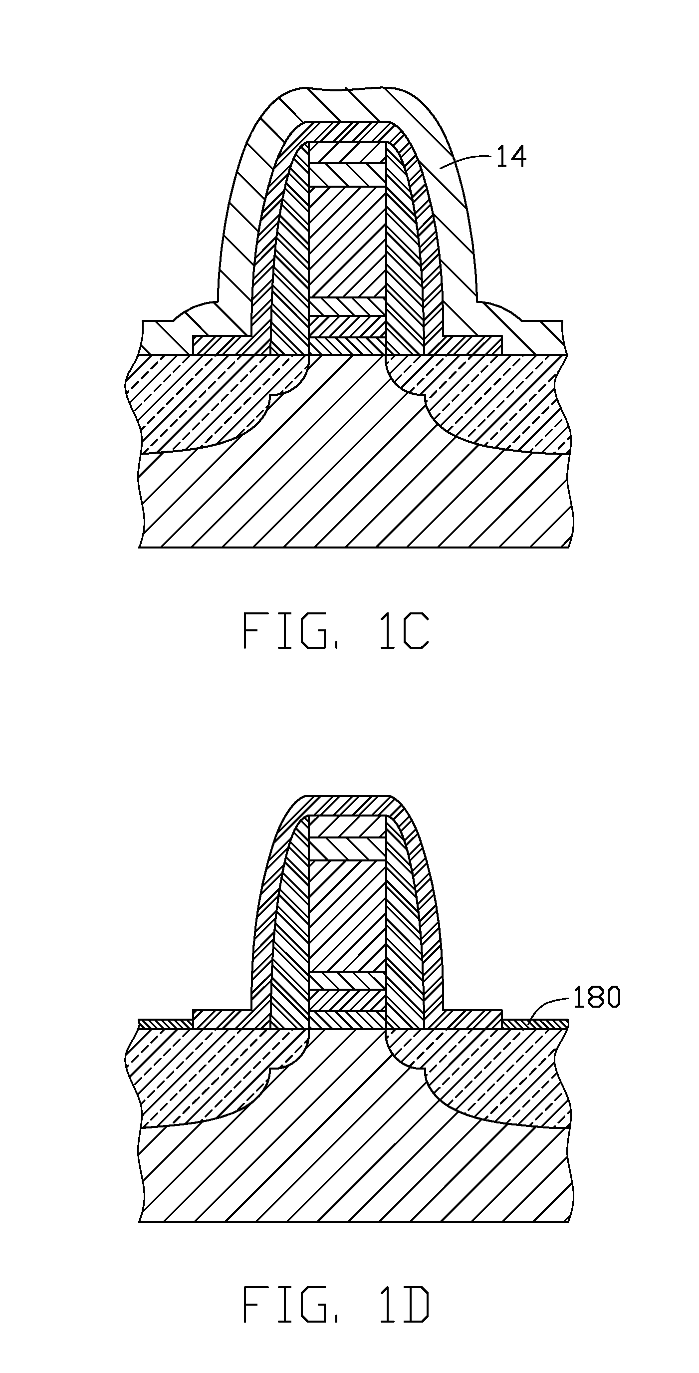
[0026] Then, as shown in FIG. 1C, a stress film 14 for implementing the stress memorization technique is deposited on the inner layer 160 of the second spacer 16 and the source/drain structure 18. For example, the stress film 14 is a silicon nitride film. Alternatively, the stress film 14 is a composite film including a buffer oxide film and a silicon nitride film. According to various depositing conditions, the silicon nitride film can be controlled to have the function of a tensile stress film or a compressive stress film. For example, the compressive stress film for increasing the hole mobility of the P-channel may be simply formed by a chemical vapor deposition (CVD) process. Whereas, the tensile stress film for increasing the electron mobility of the N-channel is formed by a plurality of deposition and curing cycle processes. After the step of depositing the stress film 14, the LDD region 17 and the source/drain structure 18 in the amorphous phase are subject to an annealing process. Due to the annealing process, the amorphous phases of the LDD region 17 and the source/drain structure 18 are transformed and restored into the crystal phases. Meanwhile, the stress provided by the stress film 14 can be effectively memorized.
[0027] Then, as shown in FIG. 1D, a wet etching process is performed to remove the stress film 14, thereby exposing the L-shaped silicon dioxide layer. In a case that the stress film 14 is made of silicon nitride, a hot phosphoric acid (H.sub.3PO.sub.4) solution may be used as an etchant solution. Then, a self-aligned silicidation process is performed to form a salicide layer 180 on the source/drain structure 18. Alternatively, the salicide layer 180 may be formed immediately after the second spacer 16 is formed.
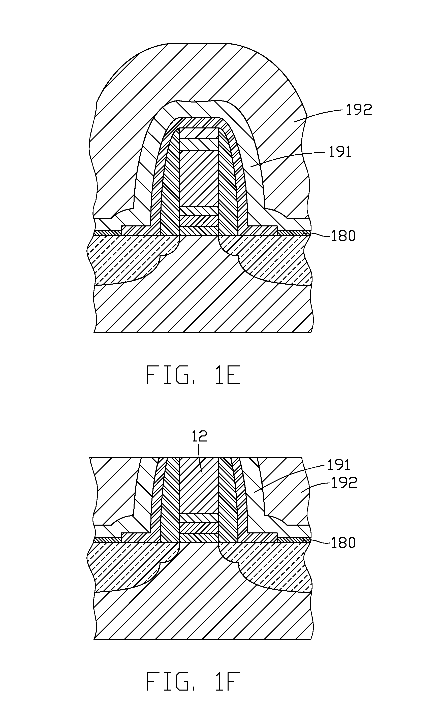
[0028] Then, as shown in FIG. 1E, a contact etch stop layer (CESL) 191 and an interlayer dielectric layer (ILD) 192 are formed over the resulting structure of FIG. 1D.
[0029] Then, as shown in FIG. 1F, a chemical mechanical polishing (CMP) process is performed to remove a portion of the contact etch stop layer 191, a portion of the interlayer dielectric layer 192 and the hard mask layer 13, so that the polysilicon dummy gate 12 is exposed.
[0030] Then, a wet etching process is performed to remove the exposed polysilicon dummy gate 12, thereby creating a trench. Then, a metal gate structure is filled into the trench. As shown in FIG. 1F, the metal gate structure comprises an etch stop layer 120, a work function metal layer 121 and a metal gate 122. Meanwhile, a metal-oxide-semiconductor field-effect transistor with a gate-last high-k metal gate (HKMG) is fabricated. For example, the etch stop layer 120 is made of made of titanium nitride (TiN). For the P-channel MOSFET, the work function metal layer 121 is made of titanium nitride (TiN). For the N-channel MOSFET, the work function metal layer 121 is made of titanium aluminum (TiAl). The metal gate 122 is made of aluminum (Al).
[0031] In the above embodiment, since the silicon nitride layer 161 of the second spacer 16 is removed by the back-etch process, the stress provided to the amorphous phases of the LDD region 17 and the source/drain structure 18 can be efficiently memorized. Therefore, the efficacy of adjusting mobility of the channel of the metal-oxide-semiconductor field-effect transistor will be enhanced.
[0032] In the above embodiment, the metal-oxide-semiconductor field-effect transistor is fabricated by a gate-last process. Nevertheless, the metal-oxide-semiconductor field-effect transistor may be fabricated by a gate-first process. The steps of the gate-first process are substantially identical to those of the gate-first process except that the steps of removing the polysilicon dummy gate 12 and filling the work function metal layer 121 and a metal gate 122 are omitted.
[0033] In some embodiments, the high-K dielectric layer 101 is not previously formed in the step as shown in FIG. 1A. After the polysilicon dummy gate 12 is removed, the high-K dielectric layer 101, the etch stop layer 120, the work function metal layer 121 and the metal gate 122 are sequentially filled into the trench.
[0034] In the above embodiment, the salicide layer 180 is formed on the source/drain structure 18 after the stress film 14 is removed. It is noted that the sequence of forming the salicide layer may be varied according to the practical requirements. For example, as shown in FIG. 2, after a contact hole 20 is formed, a surface of the source/drain structure 18 is exposed. Then, a salicide layer 180 is formed on the exposed surface of the source/drain structure 18. Under this circumstance, amorphous phases of the LDD region 17 and the source/drain structure 18 have better stress memorization efficacy.
[0035] While the invention has been described in terms of what is presently considered to be the most practical and preferred embodiments, it is to be understood that the invention needs not be limited to the disclosed embodiment. On the contrary, it is intended to cover various modifications and similar arrangements included within the spirit and scope of the appended claims which are to be accorded with the broadest interpretation so as to encompass all such modifications and similar structures.
* * * * *
D00000
D00001
D00002
D00003
D00004
XML
uspto.report is an independent third-party trademark research tool that is not affiliated, endorsed, or sponsored by the United States Patent and Trademark Office (USPTO) or any other governmental organization. The information provided by uspto.report is based on publicly available data at the time of writing and is intended for informational purposes only.
While we strive to provide accurate and up-to-date information, we do not guarantee the accuracy, completeness, reliability, or suitability of the information displayed on this site. The use of this site is at your own risk. Any reliance you place on such information is therefore strictly at your own risk.
All official trademark data, including owner information, should be verified by visiting the official USPTO website at www.uspto.gov. This site is not intended to replace professional legal advice and should not be used as a substitute for consulting with a legal professional who is knowledgeable about trademark law.