Thermoelectric Conversion Material And Producing Method Thereof; And Thermoelectric Conversion Element Using The Same
Park; Cheol-Hee ; et al.
U.S. patent application number 13/531186 was filed with the patent office on 2012-12-27 for thermoelectric conversion material and producing method thereof; and thermoelectric conversion element using the same. Invention is credited to Seung-Tae Hong, Tae-Hoon Kim, Won-Jong Kwon, Cheol-Hee Park, Se-Hui Sohn.
| Application Number | 20120326100 13/531186 |
| Document ID | / |
| Family ID | 41721647 |
| Filed Date | 2012-12-27 |


View All Diagrams
| United States Patent Application | 20120326100 |
| Kind Code | A1 |
| Park; Cheol-Hee ; et al. | December 27, 2012 |
THERMOELECTRIC CONVERSION MATERIAL AND PRODUCING METHOD THEREOF; AND THERMOELECTRIC CONVERSION ELEMENT USING THE SAME
Abstract
Thermoelectric conversion materials, expressed by the following formula: Bi.sub.1-xM.sub.xCu.sub.wO.sub.a-yQ1.sub.yTe.sub.b-zQ2.sub.z. Here, M is at least one element selected from the group consisting of Ba, Sr, Ca, Mg, Cs, K, Na, Cd, Hg, Sn, Pb, Mn, Ga, In, Tl, As and Sb; Q1 and Q2 are at least one element selected from the group consisting of S, Se, As and Sb; x, y, z, w, a, and b are 0.ltoreq.x<1, 0<w.ltoreq.1, 0.2<a<4, 0.ltoreq.y<4, 0.2<b<4 and 0.ltoreq.z<4. These thermoelectric conversion materials may be used for thermoelectric conversion elements, where they may replace thermoelectric conversion materials in common use, or be used along with thermoelectric conversion materials in common use.
| Inventors: | Park; Cheol-Hee; (Daejeon, KR) ; Sohn; Se-Hui; (Daejeon, KR) ; Hong; Seung-Tae; (Daejeon, KR) ; Kwon; Won-Jong; (Daejeon, KR) ; Kim; Tae-Hoon; (Seoul, KR) |
| Family ID: | 41721647 |
| Appl. No.: | 13/531186 |
| Filed: | June 22, 2012 |
Related U.S. Patent Documents
| Application Number | Filing Date | Patent Number | ||
|---|---|---|---|---|
| 12906917 | Oct 18, 2010 | 8226843 | ||
| 13531186 | ||||
| PCT/KR2008/007041 | Nov 28, 2008 | |||
| 12906917 | ||||
| Current U.S. Class: | 252/519.4 |
| Current CPC Class: | H01B 1/08 20130101; H01L 31/072 20130101; H01L 35/18 20130101; C09K 11/881 20130101; H01L 31/032 20130101; H01L 31/0725 20130101; C09K 11/885 20130101; H01L 35/22 20130101; H01B 1/10 20130101; H01L 31/0272 20130101; Y02E 10/50 20130101; H01L 35/16 20130101 |
| Class at Publication: | 252/519.4 |
| International Class: | H01L 31/0272 20060101 H01L031/0272 |
Foreign Application Data
| Date | Code | Application Number |
|---|---|---|
| Aug 29, 2008 | KR | 10-2008-0085240 |
| Oct 6, 2008 | KR | 10-2008-0097779 |
| Nov 11, 2008 | KR | 10-2008-0111557 |
Claims
1-19. (canceled)
20. The thermoelectric conversion materials having a natural super-lattice structure in which Cu.sub.2Te.sub.2 layers alternate with Bi.sub.2O.sub.2 layers along a c-crystalline axis, wherein at least one of Bi, O and Te is partially substituted by M, Q1 and Q2, respectively, or Cu is partially deficient, where M is at least one element selected from the group consisting of Ba, Sr, Ca, Mg, Cs, K, Na, Cd, Hg, Sn, Pb, Mn, Ga, In, Tl, As and Sb; Q1 and Q2 are at least one element selected from the group consisting of S, Se, As and Sb.
21. The thermoelectric conversion materials according to claim 20, wherein, when each of x, y and z is a ratio of the substitution by M, Q1 and Q2 in Bi, O and Te, respectively, and w is a ratio of the deficiency in Cu, the x, y, z and w satisfy the following relations: 0.ltoreq.x.ltoreq.1/2, 0.ltoreq.y.ltoreq.1/2 and 0.ltoreq.z.ltoreq.1/2.
22. The thermoelectric conversion materials according to claim 20, wherein the x, y and z satisfy the following relations: x=0, y=0 and z=0.
23. The thermoelectric conversion materials according to claim 20, wherein the Q1 and Q2 are respectively Se or Sb.
24. The thermoelectric conversion materials according to claim 23, wherein the x, y, z and w satisfy the following relations: 0.ltoreq.x<0.15, 0.ltoreq.y<0.2, 0.ltoreq.z<0.5 and 0.ltoreq.w.ltoreq.0.2.
25. The thermoelectric conversion materials according to claim 23, wherein the M is any one selected from the group consisting of Sr, Cd, Pb and Tl.
26. The thermoelectric conversion materials according to claim 23, wherein the Q1 and Q2 are respectively Se or Sb.
27. The thermoelectric conversion materials according to claim 23, wherein the x, y, z and w satisfy the following relations: 0.ltoreq.x<0.15, 0.ltoreq.y<0.2, 0.ltoreq.z<0.5 and 0.ltoreq.w.ltoreq.0.2; the M is any one selected from the group consisting of Sr, Cd, Pb and Tl; and the Q1 and Q2 are respectively Se or Sb.
28. The thermoelectric conversion materials according to claim 27, wherein the x, y, z and w satisfy the following relations: 0<x<0.15, y=0, z=0 and w=0; and the M is any one selected from the group consisting of Sr, Cd, Pb and Tl.
29. The thermoelectric conversion materials according to claim 27, wherein the x, y, z and w satisfy the following relations: x=0, y=0, 0<z.ltoreq.0.5 and w=0; and the Q2 is Se or Sb.
30. A method for producing thermoelectric conversion materials, wherein powders of Bi.sub.2O.sub.3, Bi, Cu and Te are mixed and then sintered to produce the thermoelectric conversion materials defined in the claim 20.
31. A method for producing thermoelectric conversion materials, wherein Bi.sub.2O.sub.3, Bi, Cu, Te, and at least one selected from the group consisting of Ba, Sr, Ca, Mg, Cs, K, Na, Cd, Hg, Sn, Pb, Mn, Ga, In, Tl, As and Sb, or their oxides, are mixed and then sintered to produce the thermoelectric conversion materials defined in the claim 20.
32. A method for producing thermoelectric conversion materials, wherein Bi.sub.2O.sub.3, Bi, Cu, and Te are mixed with at least one selected from the group consisting of S, Se, As and Sb, or their oxides, and then at least one selected from the group consisting of Ba, Sr, Ca, Mg, Cs, K, Na, Cd, Hg, Sn, Pb, Mn, Ga, In, Tl, As and Sb, or their oxides, are selectively further mixed thereto and then sintered to produce the thermoelectric conversion materials defined in the claim 20.
33. The method for producing thermoelectric conversion materials according to claim 30, wherein the sintering process is executed at a temperature of 400 to 570.degree. C.
34. The method for producing thermoelectric conversion materials according to claim 31, wherein the sintering process is executed at a temperature of 400 to 570.degree. C.
35. The method for producing thermoelectric conversion materials according to claim 32, wherein the sintering process is executed at a temperature of 400 to 570.degree. C.
36. A thermoelectric conversion element, which includes the thermoelectric conversion materials defined in claim 20.
37. The thermoelectric conversion materials having a natural super-lattice structure in which BiTeCu layers alternate with O layers along a c-crystalline axis, wherein at least one of Bi, O and Te is partially substituted by M, Q1 and Q2, respectively, or Cu is partially deficient, where M is at least one element selected from the group consisting of Ba, Sr, Ca, Mg, Cs, K, Na, Cd, Hg, Sn, Pb, Mn, Ga, In, Tl, As and Sb; Q1 and Q2 are at least one element selected from the group consisting of S, Se, As and Sb.
38. The thermoelectric conversion materials according to claim 37, wherein, when each of x, y and z is a ratio of the substitution by M, Q1 and Q2 in Bi, O and Te, respectively, and w is a ratio of the deficiency in Cu, the x, y, z and w satisfy the following relations: 0.ltoreq.x.ltoreq.1/2, 0.ltoreq.y.ltoreq.1/2 and 0.ltoreq.z.ltoreq.1/2.
39. The thermoelectric conversion materials according to claim 37, wherein the x, y and z satisfy the following relations: x=0, y=0 and z=0.
40. The thermoelectric conversion materials according to claim 37, wherein the x, y and z satisfy the following relation: x+y+z>0.
41. The thermoelectric conversion materials according to claim 40, wherein the x, y, z and w satisfy the following relations: 0.ltoreq.x<0.15, 0.ltoreq.y<0.2, 0.ltoreq.z<0.5 and 0.ltoreq.w.ltoreq.0.2.
42. The thermoelectric conversion materials according to claim 40, wherein the M is any one selected from the group consisting of Sr, Cd, Pb and Tl.
43. The thermoelectric conversion materials according to claim 40, wherein the Q1 and Q2 are respectively Se or Sb.
44. The thermoelectric conversion materials according to claim 40, wherein the x, y, z and w satisfy the following relations: 0.ltoreq.x<0.15, 0.ltoreq.y<0.2, 0.ltoreq.z<0.5 and 0.ltoreq.w.ltoreq.0.2; the M is any one selected from the group consisting of Sr, Cd, Pb and Tl; and the Q1 and Q2 are respectively Se or Sb.
45. The thermoelectric conversion materials according to claim 44, wherein the x, y, z and w satisfy the following relations: 0<x<0.15, y=0, z=0 and w=0; and the M is any one selected from the group consisting of Sr, Cd, Pb and Tl.
46. The thermoelectric conversion materials according to claim 44, wherein the x, y, z and w satisfy the following relations: x=0, y=0, 0<z.ltoreq.0.5 and w=0; and the Q2 is Se or Sb.
47. A method for producing thermoelectric conversion materials, wherein powders of Bi.sub.2O.sub.3, Bi, Cu and Te are mixed and then sintered to produce the thermoelectric conversion materials defined in the claim 37.
48. A method for producing thermoelectric conversion materials, wherein Bi.sub.2O.sub.3, Bi, Cu, Te, and at least one selected from the group consisting of Ba, Sr, Ca, Mg, Cs, K, Na, Cd, Hg, Sn, Pb, Mn, Ga, In, Tl, As and Sb, or their oxides, are mixed and then sintered to produce the thermoelectric conversion materials defined in the claim 37.
49. A method for producing thermoelectric conversion materials, wherein Bi.sub.2O.sub.3, Bi, Cu, and Te are mixed with at least one selected from the group consisting of S, Se, As and Sb, or their oxides, and then at least one selected from the group consisting of Ba, Sr, Ca, Mg, Cs, K, Na, Cd, Hg, Sn, Pb, Mn, Ga, In, Tl, As and Sb, or their oxides, are selectively further mixed thereto and then sintered to produce the thermoelectric conversion materials defined in the claim 37.
50. The method for producing thermoelectric conversion materials according to claim 47, wherein the sintering process is executed at a temperature of 400 to 570.degree. C.
51. The method for producing thermoelectric conversion materials according to claim 48, wherein the sintering process is executed at a temperature of 400 to 570.degree. C.
52. The method for producing thermoelectric conversion materials according to claim 49, wherein the sintering process is executed at a temperature of 400 to 570.degree. C.
53. A thermoelectric conversion element, which includes the thermoelectric conversion materials defined in claim 37.
Description
CROSS REFERENCE TO RELATED APPLICATIONS
[0001] This application is a continuation of U.S. Ser. No. 12/906,917, filed on Oct. 18, 2010, which is a continuation of International Application No. PCT/KR2008/007041 filed Nov. 28, 2008, which claims priorities to Korean Patent Applications Nos. 10-2008-0085240, 10-2008-0097779 and 10-2008-0111557 filed in Republic of Korea on Aug. 29, 2008, Oct. 6, 2008 and Nov. 11, 2008, respectively, the entire contents of which are incorporated herein by reference.
TECHNICAL FIELD
[0002] The present invention provides new thermoelectric conversion material, their method of preparation, and thermoelectric conversion elements by using the same.
BACKGROUND OF THE INVENTION
[0003] The thermoelectric conversion element is applied to thermoelectric conversion power generation or thermoelectric conversion cooling. For example, for the thermoelectric conversion power generation, a temperature difference is applied to the thermoelectric conversion element to generate thermoelectromotive force, and then the thermoelectromotive force is used to convert thermal energy into electric energy.
[0004] Energy conversion efficiency of the thermoelectric conversion element depends on ZT value that is a performance index of thermoelectric conversion material. ZT value is determined by Seebeck coefficient, electric conductivity and thermal conductivity. In more detail, ZT value is in proportion to electric conductivity and square of Seebeck coefficient and in reverse proportion to thermal conductivity. Thus, in order to enhance the energy conversion efficiency of a thermoelectric conversion element, it is required to develop thermoelectric conversion materials with high Seebeck coefficient, high electric conductivity or low thermal conductivity.
DISCLOSURE
Technical Problem
[0005] An object of the present invention is to provide new thermoelectric conversion material having excellent thermoelectric conversion performance.
[0006] Another object of the present invention is to provide a method for producing the above new thermoelectric conversion material.
[0007] Furthermore, another object of the present invention is to provide a thermoelectric conversion element using the new thermoelectric conversion material.
Technical Solution
[0008] As a result of the research for thermoelectric conversion material, compositions of the formula 1 are proposed in the present invention. It was found that these new compounds may be used as thermoelectric conversion materials of thermoelectric conversion elements, and so on.
Bi.sub.1-xM.sub.xCu.sub.wO.sub.a-yQ1.sub.yTe.sub.b-zQ2.sub.z Formula 1
[0009] where M is at least one element selected from the group consisting of Ba, Sr, Ca, Mg, Cs, K, Na, Cd, Hg, Sn, Pb, Mn, Ga, In, Tl, As and Sb; Q1 and Q2 are at least one element selected from the group consisting of S, Se, As and Sb with 0.ltoreq.x<1, 0<w.ltoreq.1, 0.2<a<4, 0.ltoreq.y<4, 0.2<b<4 and 0.ltoreq.z<4.
[0010] According to the present invention, x, y and z of the formula 1 are x+y+z>0, and a, y, b and z are preferably a=1, 0.ltoreq.y<1, b=1 and 0.ltoreq.z<1, respectively.
[0011] In other case, x, w, a, y, b and z are preferably 0.ltoreq.x<0.15, 0.8.ltoreq.w<1, a=1, 0.ltoreq.y<0.2, b=1 and 0.ltoreq.z<0.5, respectively. Here, M is preferably any one selected from the group consisting of Sr, Cd, Pb and Tl, and Q1 and Q2 are preferably Se or Sb, respectively.
[0012] In another aspect of the present invention, it provides methods for producing thermoelectric conversion materials expressed by the above formula 1 by heating mixtures of Bi.sub.2O.sub.3, Bi, Cu and Te.
[0013] Alternatively, the present invention provides methods for producing thermoelectric conversion materials expressed by the formula 1 by heating mixtures of Bi.sub.2O.sub.3, Bi, Cu, Te, and at least one selected from the group consisting of elemental Ba, Sr, Ca, Mg, Cs, K, Na, Cd, Hg, Sn, Pb, Mn, Ga, In, Tl, As and Sb, or their oxides.
[0014] Also alternatively, the present invention provides methods for producing thermoelectric conversion materials expressed by the formula 1 by heating mixtures of Bi.sub.2O.sub.3, Bi, Cu, Te, at least one selected from the group consisting of elemental S, Se, As, and Sb, or their oxides, and optionally at least one selected from the group consisting of elemental Ba, Sr, Ca, Mg, Cs, K, Na, Cd, Hg, Sn, Pb, Mn, Ga, In, Tl, As, and Sb, or their oxides.
[0015] In the method according to the present invention, the sintering process is preferably executed at temperatures of 400 to 570.degree. C.
Advantageous Effects
[0016] The new thermoelectric conversion materials of the present invention may replace thermoelectric conversion materials in common use, or be used along with thermoelectric conversion materials in common use. In particular, the thermoelectric conversion materials may be useful for thermoelectric conversion elements due to their excellent thermoelectric conversion performance.
DESCRIPTION OF DRAWINGS
[0017] Other objects and aspects of the present invention will become apparent from the following description of embodiments with reference to the accompanying drawing in which:
[0018] FIG. 1 shows Rietveld refinement profiles for BiCuOTe, comparing X-ray diffraction pattern with a calculated pattern from a structural model;
[0019] FIG. 2 shows the crystal structure of BiCuOTe;
[0020] FIG. 3 shows Rietveld refinement profiles for Bi.sub.0.98Pb.sub.0.02CuOTe, comparing X-ray diffraction pattern with a calculated pattern from a structural model;
[0021] FIG. 4 shows the crystal structure of Bi.sub.0.98Pb.sub.0.02CuOTe;
[0022] FIG. 5 shows X-ray diffraction pattern of Bi.sub.0.9Pb.sub.0.1CuOTe;
[0023] FIG. 6 shows X-ray diffraction pattern of Bi.sub.0.9Cd.sub.0.1CuOTe;
[0024] FIG. 7 shows X-ray diffraction pattern of Bi.sub.0.9Sr.sub.0.1CuOTe;
[0025] FIG. 8 shows Rietveld refinement profiles for BiCuOSe.sub.0.5Te.sub.0.5, comparing X-ray diffraction pattern with a calculated pattern from a structural model;
[0026] FIG. 9 shows the crystal structure of BiCuOSe.sub.0.5Te.sub.0.5;
[0027] FIG. 10 shows X-ray diffraction pattern of Bi.sub.0.9Tl.sub.0.1CuOTe;
[0028] FIG. 11 shows X-ray diffraction pattern of BiCuOTe.sub.0.9Sb.sub.0.1;
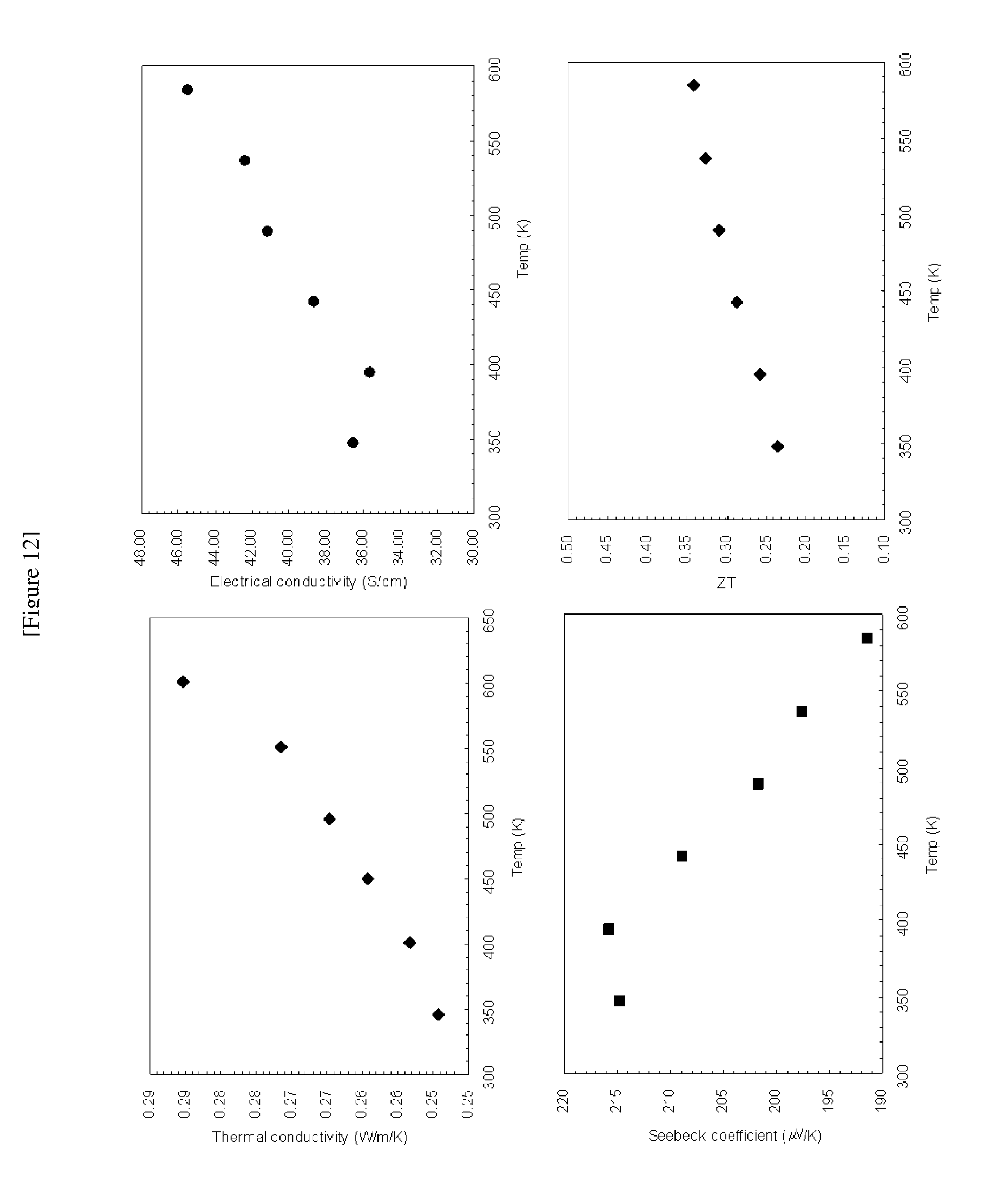
[0029] FIG. 12 shows electrical conductivities, Seebeck coefficients, thermal conductivities, and ZT values of BiCuOTe at different temperatures;
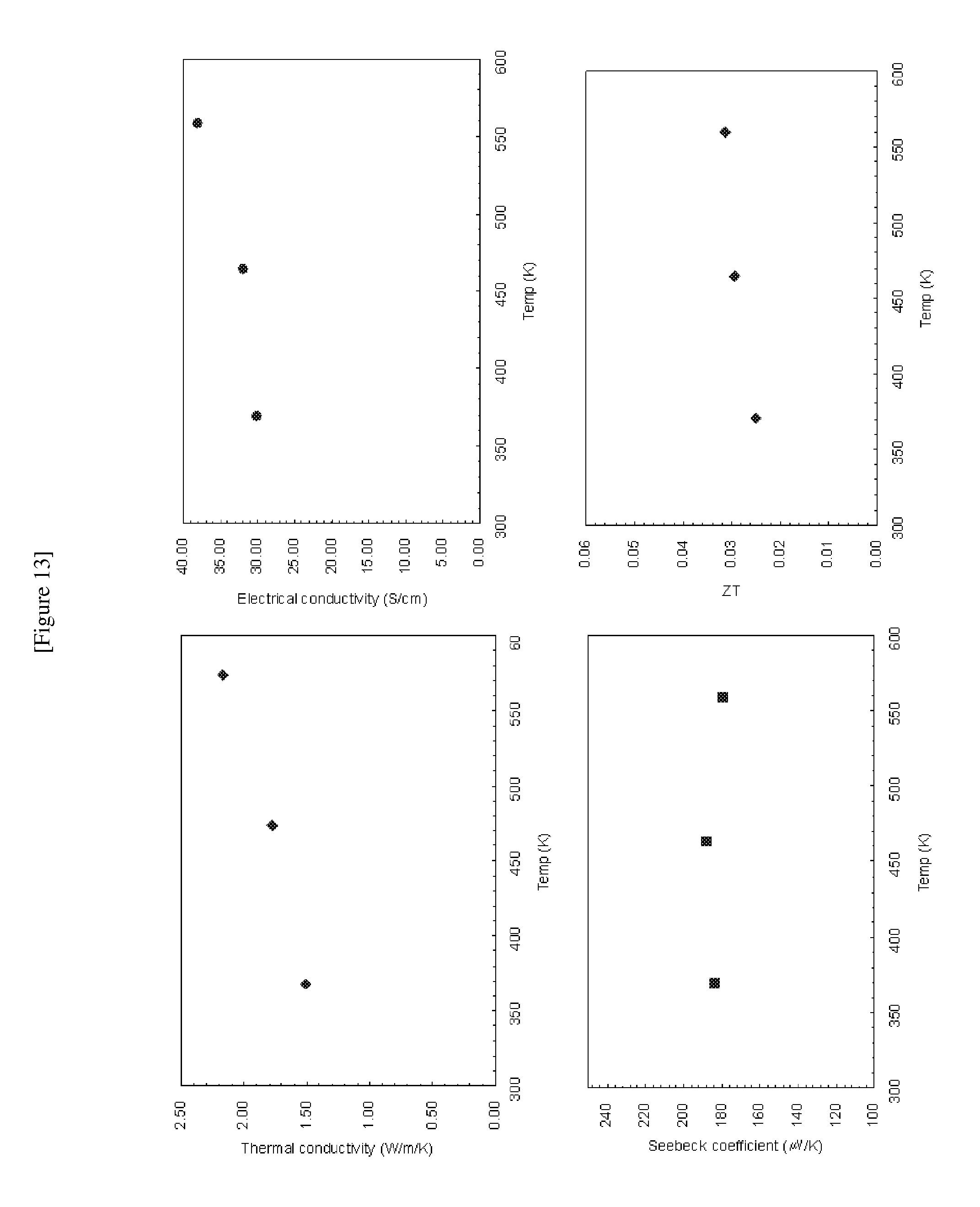
[0030] FIG. 13 shows electrical conductivities, Seebeck coefficients, thermal conductivities, and ZT values of Bi.sub.0.9Sr.sub.0.1CuOTe at different temperatures;
[0031] FIG. 14 shows electrical conductivities, Seebeck coefficients, thermal conductivities, and ZT values of Bi.sub.0.9Cd.sub.0.1CuOTe at different temperatures;
[0032] FIG. 15 shows electrical conductivities, Seebeck coefficients, thermal conductivities, and ZT values of Bi.sub.0.9Pb.sub.0.1CuOTe at different temperatures;
[0033] FIG. 16 shows electrical conductivities, Seebeck coefficients, thermal conductivities, and ZT values of Bi.sub.0.98Pb.sub.0.02CuOTe at different temperatures; and
[0034] FIG. 17 shows electrical conductivities, Seebeck coefficients, thermal conductivities, and ZT values of Bi.sub.0.9Tl.sub.0.1CuOTe at different temperatures.
BEST MODE
[0035] Compositions of the thermoelectric conversion materials of the present invention are expressed by the following formula 1.
Bi.sub.1-xM.sub.xCu.sub.wO.sub.a-yQ1.sub.yTe.sub.b-zQ2.sub.z Formula 1
[0036] In the formula 1, M is at least one element selected from the group consisting of Ba, Sr, Ca, Mg, Cs, K, Na, Cd, Hg, Sn, Pb, Mn, Ga, In, Tl, As and Sb, and Q1 and Q2 are at least one element selected from the group consisting of S, Se, As and Sb with 0.ltoreq.x<1, 0<w.ltoreq.1, 0.2<a<4, 0.ltoreq.y<4, 0.2<b<4 and 0.ltoreq.z<4.
[0037] In the formula 1, x, y, and z are preferably 0.ltoreq.x<1/2, 0.ltoreq.y.ltoreq.a/2 and 0.ltoreq.z.ltoreq.b/2, respectively.
[0038] In the formula 1, x, y, and z may be respectively x=0, y=0 and z=0. The thermoelectric conversion material of the formula 1 is preferably BiCuOTe.
[0039] In the formula 1, x, y, and z are x+y+z>0, and a, y, b and z of the formula 1 are preferably a=1, 0.ltoreq.y<1, b=1 and 0.ltoreq.z<1, respectively. In other cases, x, w, a, y, b and z may be respectively 0.ltoreq.x<0.15, 0.8.ltoreq.w.ltoreq.1, a=1, 0.ltoreq.y<0.2, b=1 and 0.ltoreq.z<0.5. Here, M is preferably any one selected from the group consisting of Sr, Cd, Pb and Tl, and Q1 and Q2 are preferably Se or Sb, respectively. More preferably, x, w, a, y, b and z of the formula 1 are respectively 0.ltoreq.x<0.15, 0.8.ltoreq.w.ltoreq.1, a=1, 0.ltoreq.y<0.2, b=1 and 0.ltoreq.z<0.5, M is any one selected from the group consisting of Sr, Cd, Pb and Tl, and Q1 and Q2 are respectively Se or Sb.
[0040] For the thermoelectric conversion materials of the formula 1, it is more preferred that x, w, a, y, b and z of the formula 1 are respectively 0<x<0.15, w=1, a=1, y=0, b=1 and z=0, and M is any one selected from the group consisting of Sr, Cd, Pb and Tl. In addition, in the formula 1 where x, w, y and z of the formula 1 are respectively x=0, w=1, a=1, y=0, b=1 and 0<z.ltoreq.0.5, and Q2 is Se or Sb, it is more preferred that x, w, a, y, b and z of the formula 1 are respectively 0<x<0.15, w=1, a=1, y=0, b=1 and z=0, and M is any one selected from the group consisting of Sr, Cd, Pb and Tl.
[0041] Meanwhile, the thermoelectric conversion materials expressed by the formula 1 may be produced by mixing powders of Bi.sub.2O.sub.3, Bi, Cu and Te and then vacuum-sintering the mixture, but the present invention is not limited thereto.
[0042] Also, the thermoelectric conversion materials expressed by the formula 1 may be produced by heating mixtures of Bi.sub.2O.sub.3, Bi, Cu, Te, and at least one selected from the group consisting of Ba, Sr, Ca, Mg, Cs, K, Na, Cd, Hg, Sn, Pb, Mn, Ga, In, Tl, As and Sb, or their oxides in an evacuated silica tube, however the present invention is not limited thereto.
[0043] In addition, the thermoelectric conversion materials expressed by the formula 1 may be produced by heating mixtures of Bi.sub.2O.sub.3, Bi, Cu, Te, at least one element selected from the group consisting of S, Se, As and Sb, or their oxides, and optionally at least one selected from the group consisting of Ba, Sr, Ca, Mg, Cs, K, Na, Cd, Hg, Sn, Pb, Mn, Ga, In, Tl, As, and Sb, or their oxides in an evacuated silica tube, however the present invention is not limited thereto.
[0044] The thermoelectric conversion materials of the present invention may be produced by sintering mixtures in a flowing gas such as Ar, He or N.sub.2, which partially includes hydrogen or does not include hydrogen. The sintering process is preferably executed at a temperature of 400 to 750.degree. C., more preferably 400 to 570.degree. C.
[Mode for Invention]
[0045] Hereinafter, the preferred embodiment of the present invention will be described in detail based on examples. However, the embodiments of the present invention may be modified in various ways, and the scope of the present invention should not be interpreted as being limited to the examples. The embodiments of the present invention are provided just for explaining the present invention more perfectly to those having ordinary skill in the art.
Example 1
BiCuOTe
[0046] In order to prepare BiCuOTe, 1.1198 g of Bi.sub.2O.sub.3 (Aldrich, 99.9%, 100 mesh), 0.5022 g of Bi (Aldrich, 99.99%, <10 m), 0.4581 g of Cu (Aldrich, 99.7%, 3 m), and 0.9199 g of Te (Aldrich, 99.99%, .about.100 mesh) were well mixed by using agate mortar, and then heated in an evacuated silica tube at 510.degree. C. for 15 hours, thereby obtaining BiCuOTe powder.
[0047] The powder X-ray diffraction (XRD) data were collected at room temperature on a Bragg-Brentano diffractometer (Bruker Advance D8 XRD) with a Cu X-ray tube (.lamda.=1.5406 .ANG., 50 kV, 40 mA). The step size was 0.02 degree.
[0048] TOPAS program (R. W. Cheary, A. Coelho, J. Appl. Crystallogr. 25 (1992) 109-121; Bruker AXS, TOPAS 3, Karlsruhe, Germany (2000)) was used in order to determine the crystal structure of the obtained material. The analysis results are shown in Table 1 and FIG. 2.
TABLE-US-00001 TABLE 1 Atom site x y z Occup. Beq Bi 2c 0.25 0.25 0.37257(5) 1 0.56(1) Cu 2a 0.75 0.25 0 1 0.98(3) O 2b 0.75 0.25 0.5 1 0.26(12) Te 2c 0.25 0.25 0.81945(7) 1 0.35(1)
[0049] Crystallographic data obtained from Rietveld refinement of BiCuOTe [Space group I4/nmm (No. 129), a=4.04138(6) .ANG., c=9.5257(2) .ANG.]
[0050] FIG. 1 shows a Rietveld refinement profile that compares observed X-ray diffraction pattern of BiCuOTe with a calculated X-ray diffraction pattern from a structural model. FIG. 1 shows that the measured pattern well agrees with the calculated pattern according to Table 1, which implies that the material obtained in this example is BiCuOTe.
[0051] As shown in FIG. 2, the BiCuOTe exhibits a natural super-lattice structure in which Cu.sub.2Te.sub.2 layers and Bi.sub.2O.sub.2 layers are repeated along a c-crystalline axis.
Example 2
Bi.sub.0.98Pb.sub.0.02CuOTe
[0052] In order to prepare Bi.sub.0.98Pb.sub.0.02CuOTe, 2.5356 g of Bi.sub.2O.sub.3 (Aldrich, 99.9%, 100 mesh), 1.1724 g of Bi (Aldrich, 99.99%, <10 m), 1.0695 g of Cu (Aldrich, 99.7%, 3 m), 0.0751 g of PbO (Canto, 99.5%), and 2.1475 g of Te (Aldrich, 99.99%, .about.100 mesh) were well mixed by using agate mortar, and then heated in an evacuated silica tube at 510.degree. C. for 15 hours, thereby obtaining Bi.sub.0.98Pb.sub.0.02CuOTe powder.
[0053] The powder X-ray diffraction (XRD) data were collected at room temperature on a Bragg-Brentano diffractometer (Bruker D4-Endeavor XRD) with a Cu X-ray tube (.lamda.=1.5406 .ANG., 50 kV, 40 mA). The step size was 0.02 degree.
[0054] TOPAS program (R. W. Cheary, A. Coelho, J. Appl. Crystallogr. 25 (1992) 109-121; Bruker AXS, TOPAS 3, Karlsruhe, Germany (2000)) was used in order to determine the crystal structure of the obtained material. The analysis results are shown in Table 2 and FIG. 4.
TABLE-US-00002 TABLE 2 Atom site x y z Occup. Beq. Bi 2c 0.25 0.25 0.37225(12) 0.98 0.59(4) Pb 2c 0.25 0.25 0.37225(12) 0.02 0.59(4) Cu 2a 0.75 0.25 0 1 1.29(10) O 2b 0.75 0.25 0.5 1 0.9(4) Te 2c 0.25 0.25 0.81955(17) 1 0.55(5)
Crystallographic data obtained from Rietveld refinement of Bi.sub.0.98Pb.sub.0.02CuOTe [Space group P4/nmm (No. 129), a=4.04150(4) .ANG., c=9.53962(13) .ANG.]
[0055] FIG. 3 shows a Rietveld refinement profile that compares observed X-ray diffraction pattern of Bi.sub.0.98Pb.sub.0.02CuOTe with calculated pattern of a structural model. FIG. 3 shows that the measured pattern well agrees with the calculated pattern according to Table 2, which implies that the material obtained in this example is Bi.sub.0.98Pb.sub.0.02CuOTe.
[0056] As shown in FIG. 4, the Bi.sub.0.98Pb.sub.0.02CuOTe exhibits a natural super-lattice structure in which Cu.sub.2Te.sub.2 layers and (Bi,Pb).sub.2O.sub.2 layers where Pb is partially substituted in place of Bi are repeated along a c-crystalline axis.
Example 3
Bi.sub.0.9Pb.sub.0.1CuOTe
[0057] In order to prepare Bi.sub.0.9Pb.sub.0.1CuOTe, 1.2721 g of Bi.sub.2O.sub.3 (Aldrich, 99.9%, 100 mesh), 0.6712 g of Bi (Aldrich, 99.99%, <10 m), 0.6133 g of Cu (Aldrich, 99.7%, 3 m), 0.215 g of PbO (Canto, 99.5%), and 1.2294 g of Te (Aldrich, 99.99%, .about.100 mesh) were well mixed by using agate mortar, and then heated in an evacuated silica tube at 510.degree. C. for 15 hours, thereby obtaining Bi.sub.0.9Pb.sub.0.1CuOTe powder.
[0058] X-ray diffraction analysis was conducted for the sample in the same way as the example 2. As shown in FIG. 5, the material obtained in the example 3 was identified as Bi.sub.0.9Pb.sub.0.1CuOTe.
Example 4
Bi.sub.0.9Cd.sub.0.1CuOTe
[0059] In order to prepare Bi.sub.0.9Cd.sub.0.1CuOTe, 1.3018 g of Bi.sub.2O.sub.3 (Aldrich, 99.9%, 100 mesh), 0.6869 g of Bi (Aldrich, 99.99%, <10 m), 0.6266 g of Cu (Aldrich, 99.7%, 3 m), 0.1266 g of CdO (Strem, 99.999%), and 1.2582 g of Te (Aldrich, 99.99%, .about.100 mesh) were well mixed by using agate mortar, and then heated in an evacuated silica tube at 510.degree. C. for 15 hours, thereby obtaining Bi.sub.0.9Cd.sub.0.1CuOTe powder.
[0060] X-ray diffraction analysis was conducted for the sample in the same way as the example 2. As shown in FIG. 6, the material obtained in the example 4 was identified as Bi.sub.0.9Cd.sub.0.1CuOTe.
Example 5
Bi.sub.0.9Sr.sub.0.1CuOTe
[0061] In order to prepare Bi.sub.0.9Sr.sub.0.1CuOTe, 1.0731 g of Bi.sub.2O.sub.3 (Aldrich, 99.9%, 100 mesh), 0.5662 g of Bi (Aldrich, 99.99%, <10 m), 0.5165 g of Cu (Aldrich, 99.7%, 3 m), 1.0372 g of Te (Aldrich, 99.99%, .about.100 mesh), and 0.0842 g of SrO were well mixed by using agate mortar. Here, SrO was obtained by thermally treating SrCO.sub.3 (Alfa, 99.994%) at 1125.degree. C. for 12 hours in the air. The material obtained by thermal treatment was confirmed as SrO by X-ray diffraction analysis.
[0062] The mixture was then heated in an evacuated silica tube at 510.degree. C. for 15 hours, thereby obtaining Bi.sub.0.9Sr.sub.0.1CuOTe powder.
[0063] The powder X-ray diffraction (XRD) data were collected at room temperature on a Bragg-Brentano diffractometer (Bruker D8 Advance XRD) with a Cu X-ray tube (.lamda.=1.5406 .ANG., 50 kV, 40 mA). The step size was 0.02 degree. FIG. 7 shows that the material obtained in the example 5 is Bi.sub.0.9Sr.sub.0.1CuOTe.
Example 6
BiCuOSe.sub.0.5Te.sub.0.5
[0064] In order to prepare BiCuOSe.sub.0.5Te.sub.0.5, 1.9822 g of Bi.sub.2O.sub.3 (Aldrich, 99.9%, 100 mesh), 0.889 g of Bi (Aldrich, 99.99%, <10 m), 0.811 g of Cu (Aldrich, 99.7%, 3 m), 0.5036 g of Se (Aldrich, 99.99%), and 0.8142 g of Te (Aldrich, 99.99%, .about.100 mesh) were well mixed by using agate mortar, and then heated in an evacuated silica tube at 510.degree. C. for 15 hours, thereby obtaining BiCuOSe.sub.0.5Te.sub.0.5 powder.
[0065] The powder X-ray diffraction (XRD) data were collected at room temperature on a Bragg-Brentano diffractometer (Bruker D4-Endeavor XRD) with a Cu X-ray tube (40 kV, 40 mA). The step size was 0.02 degree. At this time, variable 6 mm slit was used as a divergence slit. The results are shown in FIG. 8. Crystal structure analysis was executed in the same way as the example 2. The analysis results are shown in Table 3 and FIG. 9.
TABLE-US-00003 TABLE 3 Atom site x y z Occup. Beq. Bi 2c 0.25 0.25 0.36504(9) 1 0.86(2) Cu 2a 0.75 0.25 0 1 2.00(9) O 2b 0.75 0.25 0.5 1 1.9(3) Te 2c 0.25 0.25 0.82272(14) 0.5 0.61(4) Se 2c 0.25 0.25 0.82252(14) 0.5 0.55(5)
Crystallographic data obtained from Rietveld refinement of BiCuOSe.sub.0.5Te.sub.0.5 [Space group P4/nmm (No. 129), a=3.99045(11) .ANG., c=9.2357(4) .ANG.]
[0066] FIG. 8 shows that the measured pattern well agrees with the calculated pattern from the results in Table 3, and as a result the material obtained in this example is identified as BiCuOSe.sub.0.5Te.sub.0.5.
[0067] As shown in FIG. 9, the BiCuOSe.sub.0.5Te.sub.0.5 exhibits a natural super-lattice structure in which Cu.sub.2(Te,Se).sub.2 layers and Bi.sub.2O.sub.2 layers are repeated along a c-crystalline axis.
Example 7
Bi.sub.0.9Tl.sub.0.1CuOTe
[0068] In order to prepare Bi.sub.0.9Tl.sub.0.1CuOTe, 1.227 g of Bi.sub.2O.sub.3 (Aldrich, 99.9%, 100 mesh), 0.7114 g of Bi (Aldrich, 99.99%, <10 m), 0.6122 g of Cu (Aldrich, 99.7%, 3 m), 1.2293 g of Te (Aldrich, 99.99%, .about.100 mesh), and 0.22 g of Tl.sub.2O.sub.3 (Aldrich) were well mixed by using agate mortar.
[0069] The mixture was then heated in an evacuated silica tube at 510.degree. C. for 15 hours, thereby obtaining Bi.sub.0.9Tl.sub.0.1CuOTe powder.
[0070] X-ray diffraction analysis was conducted for the sample in the same way as the example 2. As shown in FIG. 10, the material obtained in the example 7 was identified as Bi.sub.0.9Tl.sub.0.1CuOTe.
Example 8
BiCuOTe.sub.0.9Sb.sub.0.1
[0071] In order to prepare BiCuOTe.sub.0.9Sb.sub.0.1, 1.4951 g of Bi.sub.2O.sub.3 (Aldrich, 99.9%, 100 mesh), 0.6705 g of Bi (Aldrich, 99.99%, <10 m), 0.6117 g of Cu (Aldrich, 99.7%, 3 m), 1.1054 g of Te (Aldrich, 99.99%, .about.100 mesh), and 0.1172 g of Sb (Kanto chemical, Cat. No. 01420-02) were well mixed by using agate mortar.
[0072] The mixture was then heated in an evacuated silica tube at 510.degree. C. for 15 hours, thereby obtaining BiCuOTe.sub.0.9Sb.sub.0.1 powder.
[0073] X-ray diffraction analysis was conducted for the sample in the same way as the example 2. As shown in FIG. 11-2, the material obtained in the example 8 was identified as BiCuOTe.sub.0.9Sb.sub.0.1.
[0074] Evaluation of Thermoelectric Conversion Performance
[0075] Powder samples were shaped into cylinders with a diameter of 4 mm and a length of 15 mm (for electrical conductivity and Seebeck coefficient measurements), and disks having a diameter of 10 mm and a thickness of 1 mm (for thermal conductivity measurements) by using CIP at the pressure of 200 MPa. Subsequently, the resultant disks and cylinders were heated in an evacuated silica tube at 510.degree. C. for 10 hours.
[0076] For the sintered cylinders, electric conductivity and Seebeck coefficient were measured by using a ZEM-2 (Ulvac-Rico, Inc.). The measurement results are shown in FIGS. 14 to 19. For example, at 346K thermal conductivities of BiCuOTe and Bi.sub.0.98Pb.sub.0.02CuOTe were measured as 0.25 W/m/K and 0.35 W/m/K, respectively, which are significantly lower than those of Bi.sub.2Te.sub.3 (1.9 W/m/K, T. M. Tritt, M. A. Subramanian, MRS Bulletin 31 (2006) 188-194) and Co.sub.4Sb.sub.12:In.sub.0.2 (2 W/m/K, T. He, J. Chen, D. Rosenfeld, M. A. Subramanian, Chem. Mater. 18 (2006) 759-762) which are representative thermoelectric conversion materials.
[0077] Meanwhile, for the sintered disks, thermal conductivity was measured by using TC-9000 (Ulvac-Rico, Inc). The measurement results are shown in FIGS. 12 to 17.
[0078] ZT value of each sample was calculated using the measured values. The calculated results are shown in FIGS. 12 to 17.
* * * * *
D00000
D00001
D00002
D00003
D00004
D00005
D00006
D00007
D00008
D00009
D00010
D00011
D00012

D00013

D00014

XML
uspto.report is an independent third-party trademark research tool that is not affiliated, endorsed, or sponsored by the United States Patent and Trademark Office (USPTO) or any other governmental organization. The information provided by uspto.report is based on publicly available data at the time of writing and is intended for informational purposes only.
While we strive to provide accurate and up-to-date information, we do not guarantee the accuracy, completeness, reliability, or suitability of the information displayed on this site. The use of this site is at your own risk. Any reliance you place on such information is therefore strictly at your own risk.
All official trademark data, including owner information, should be verified by visiting the official USPTO website at www.uspto.gov. This site is not intended to replace professional legal advice and should not be used as a substitute for consulting with a legal professional who is knowledgeable about trademark law.