Plating Method
Saito; Hirokazu ; et al.
U.S. patent application number 13/165865 was filed with the patent office on 2011-12-29 for plating method. This patent application is currently assigned to OKI SEMICONDUCTOR CO., LTD.. Invention is credited to Hirokazu Saito, Hideyuki Sameshima.
| Application Number | 20110315555 13/165865 |
| Document ID | / |
| Family ID | 45351506 |
| Filed Date | 2011-12-29 |


| United States Patent Application | 20110315555 |
| Kind Code | A1 |
| Saito; Hirokazu ; et al. | December 29, 2011 |
PLATING METHOD
Abstract
Disclosed is a plating method including: performing plating on a plating surface of a plating substrate with a cathode electrode contacting an area in an outer circumferential section of the plating substrate where the cathode electrode is to be contacted, the plating substrate being provided with a dummy plating area between the area where the cathode electrode is to be contacted and a product area on the plating surface of the plating substrate, by supplying a plating solution to the plating surface of the plating substrate and applying electric current between the cathode electrode and an anode electrode via the plating solution.
| Inventors: | Saito; Hirokazu; (Tokyo, JP) ; Sameshima; Hideyuki; (Tokyo, JP) |
| Assignee: | OKI SEMICONDUCTOR CO., LTD. Tokyo JP |
| Family ID: | 45351506 |
| Appl. No.: | 13/165865 |
| Filed: | June 22, 2011 |
| Current U.S. Class: | 205/118 |
| Current CPC Class: | C25D 7/12 20130101; C25D 17/001 20130101; C25D 5/08 20130101; C25D 17/10 20130101; C25D 5/02 20130101 |
| Class at Publication: | 205/118 |
| International Class: | C25D 5/02 20060101 C25D005/02 |
Foreign Application Data
| Date | Code | Application Number |
|---|---|---|
| Jun 23, 2010 | JP | 2010-142852 |
Claims
1. A plating method comprising: performing plating on a plating surface of a plating substrate with a cathode electrode contacting an area in an outer circumferential section of the plating substrate where the cathode electrode is to be contacted, the plating substrate being provided with a dummy plating area between the area where the cathode electrode is to be contacted and a product area on the plating surface of the plating substrate, by supplying a plating solution to the plating surface of the plating substrate and applying electric current between the cathode electrode and an anode electrode via the plating solution.
2. The plating method according to claim 1, wherein the shape of a dummy plating area is identical to a shape of an area where a plating film is formed in the product area.
3. The plating method according to claim 1, wherein the shape of the dummy plating area is rectangular.
4. The plating method according to claim 1, wherein the shape of a dummy plating area is a shape continuously surrounding a location where the cathode electrode is to be contacted.
5. The plating method according to claim 1, wherein a shape of the dummy plating area is a shape surrounding the entire product area.
Description
CROSS-REFERENCE TO RELATED APPLICATION
[0001] This application claims priority under 35 USC 119 from Japanese Patent Application No. 2010-142852 filed on Jun. 23, 2010, the disclosure of which is incorporated by reference herein.
BACKGROUND
[0002] 1. Field of the Invention
[0003] The present invention relates to a plating method, and more particularly, to a plating method for plating on a semiconductor wafer.
[0004] 2. Related Art
[0005] For plating on a semiconductor wafer, there may be cases in which an anode electrode is disposed so as to face a plating surface of the semiconductor wafer and a cathode electrode is brought into contact with an outer circumference portion of the semiconductor wafer. In such cases, plating is more easily formed in the vicinity of the cathode electrode than in the other portion, which makes it difficult to uniformly form the plating in a plane of the semiconductor wafer (Refer to Japanese Patent Application Laid-Open (JP-A) No. 2008-25000).
[0006] A major object of the present invention is to provide a plating method that can form a plating film having an excellent in-plane uniformity on a substrate to be plated.
SUMMARY
[0007] According to an aspect of the present invention, there is provided a plating method comprising: performing plating on a plating surface of a plating substrate with a cathode electrode contacting an area in an outer circumferential section of the plating substrate where the cathode electrode is to be contacted, the plating substrate being provided with a dummy plating area between the area where the cathode electrode is to be contacted and a product area on the plating surface of the plating substrate, by supplying a plating solution to the plating surface of the plating substrate and applying electric current between the cathode electrode and an anode electrode via the plating solution.
BRIEF DESCRIPTION OF THE DRAWINGS
[0008] An exemplary embodiment of the present invention will be described in detail based on the following figures, wherein:
[0009] FIG. 1 is a schematic longitudinal sectional view for explaining a plating apparatus suitable for use in embodiments of the present invention;
[0010] FIG. 2 is a schematic top view for explaining the plating apparatus suitable for use in the embodiments of the present invention, wherein a wafer holder 88 is omitted;
[0011] FIG. 3 is a schematic longitudinal sectional view for explaining a method for plating on a wafer;
[0012] FIG. 4 is a schematic plan view for explaining a plating method according to a first embodiment of the present invention;
[0013] FIG. 5 is a schematic plan view for explaining a plating method according to a second embodiment of the present invention;
[0014] FIG. 6 is a schematic plan view for explaining a plating method according to a third embodiment of the present invention;
[0015] FIG. 7 is a schematic plan view for explaining a plating method according to a fourth embodiment of the present invention; and
[0016] FIG. 8 is a schematic plan view for explaining a plating method of a comparative example.
DETAILED DESCRIPTION
[0017] Preferred embodiments according to the present invention will be described with reference to the accompanying drawings.
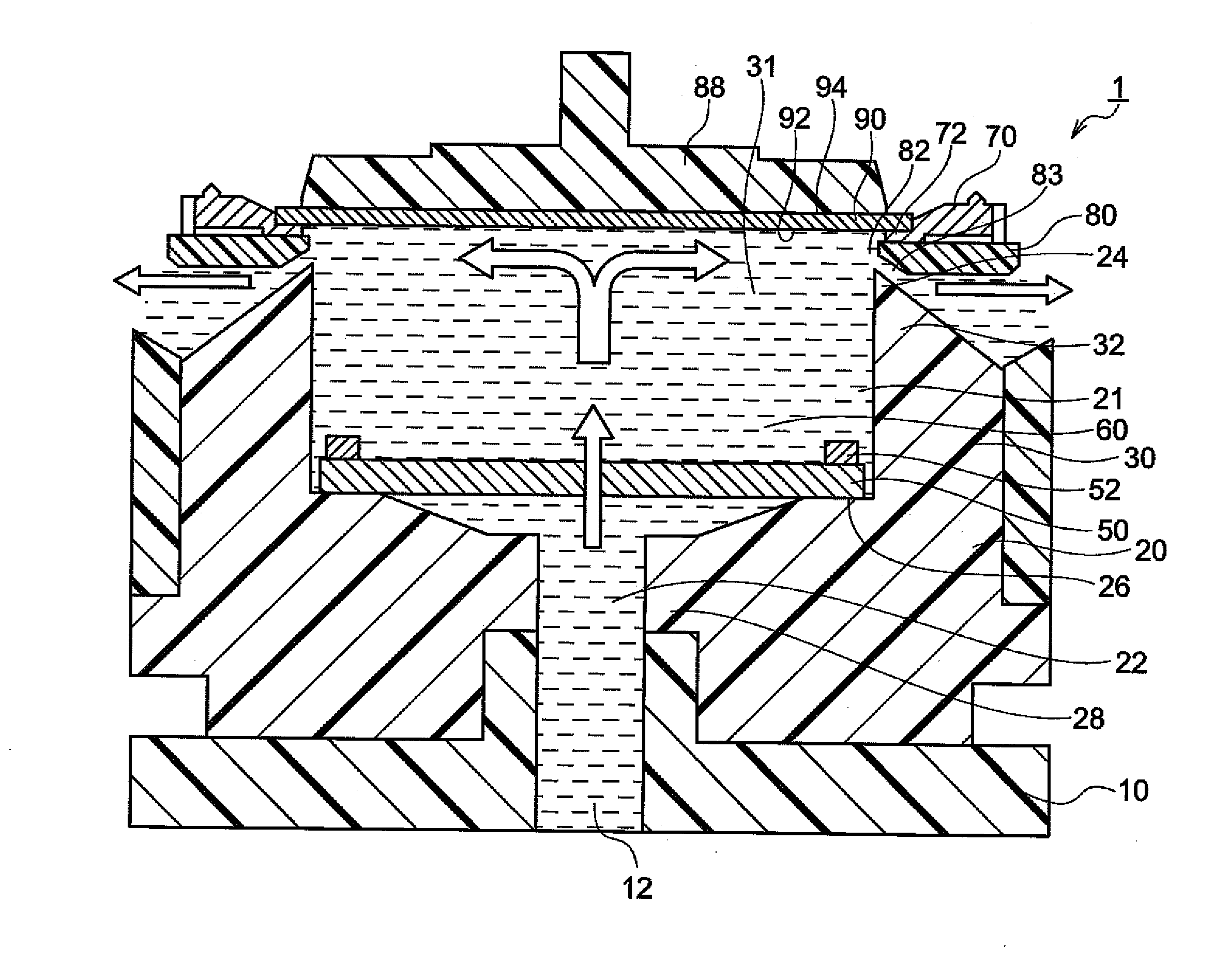
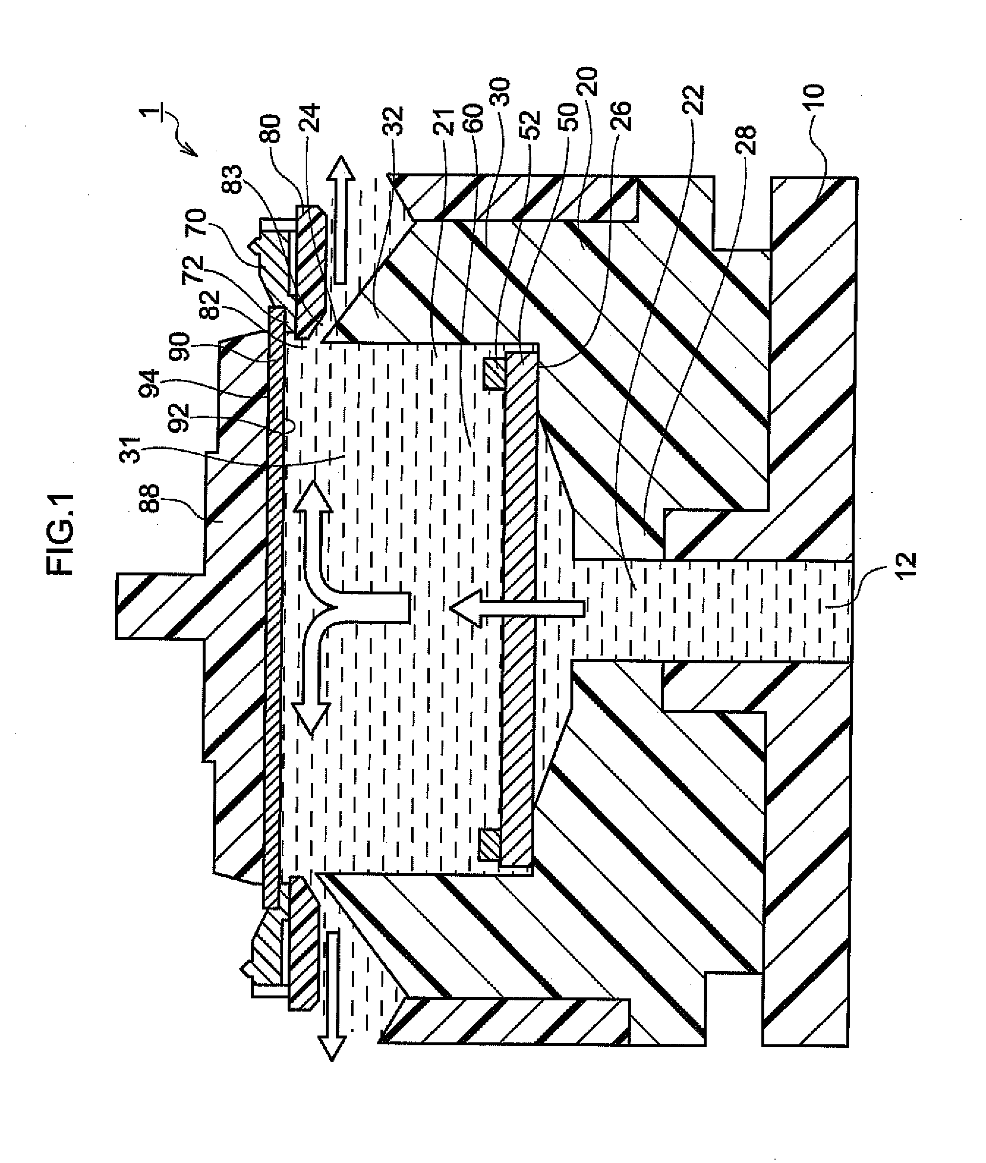
[0018] First, referring to FIGS. 1 and 2, it will be described a plating apparatus to be used in the first to fourth embodiments of the present invention. A plating apparatus 1 has a base 10, a cup 20 provided on the base 10, a ring 80 arranged over an outer circumferential section of an upper section of the cup 20, electrode pins 70 provided on the ring 80, and a wafer holder 88.
[0019] The base 10 has at a center thereof a supply port 12 which supplies plating solution 60. The cup 20 is provided on the base 10. The cup 20 has a side wall 30 and a bottom section 28. An opening section 31 surrounded by the side wall 30 is formed at an upper section of the cup 20. A plating tub 21 is defined by the side wall 30 and the bottom section 28. A supply port 22 which supplies the plating solution 60 to the plating tub 21 is formed at the center of the bottom section 28. The supply port 12 of the base 10 is in communication with the supply port 22 of the cup 20.
[0020] The electrode pins 70 are arranged at equal intervals on the ring 80 provided over the outer circumferential section of the upper section of the cup 20. The electrode pins 70 function as cathode electrodes. With respect to the electrode pins 70, it is provided three electrodes pins for a 6-inch size wafer and six electrodes pins for an 8-inch size wafer, and these are arranged at an interval of 120 degrees and an interval of 60 degrees respectively. Hereinafter, a construction in which three electrode pins are arranged will be described as an example. A wafer-mounting section 72 is provided at the tip of each of the electrodes 70. The outer circumferential section of the wafer 90 is mounted on the wafer-mounted section 72. The outer circumferential section of the wafer 90 is in contact with the wafer-mounting section 72. The wafer 90 is mounted such that a surface 92 (plating surface) of the wafer 90 faces a lower side of the sheet (the cup 20 side) so as to be opposed to the opening section 31 of the cup 20. The wafer 90 is pushed and pressed from a back surface 94 thereof by the wafer holder 88 towards the lower side of the sheet, and is fixed by the wafer holder 88 and the wafer-mounting sections 72 of the electrode pins 70. A space 82 is provided between the surface 92 of the wafer 90 and an upper edge 24 of the cup 20.
[0021] An anode plate 50 is provided on the bottom circumferential section 26 of the cup 20, and the anode plate 50 is fixed by an anode electrode 52. The anode plate 50 and the anode electrode 52 are in contact with the plating solution 60. The anode electrode 52 and the electrode pins 70 are connected to a power source for plating (not shown).
[0022] A plating solution tub (not shown) is provided at the outside of the cup 20. A pump (not shown) for supplying plating solution is provided at the supply port 12 of the base 10.
[0023] The plating solution 60 containing Cu.sup.2+ ions is supplied by the pump (not shown) to the plating tub 21 in the cup 20 from the supply port 12 of the base 10 and the supply port 22 of the cup 20, is jetted towards the center of the wafer 90 disposed over the cup 20, is contacted with the surface (plating surface) of the wafer 90, and then advances to the outer circumferential section of the wafer 90. Thereafter, the plating solution 60 overflows from the space 82 between the upper edge 24 of the cup 20 and the wafer 90, passes through a space 83 between the upper edge 24 of the cup 20 and the ring 80, and then flows to the plating solution tub (not shown) provided at the outside of the cup 20.
[0024] Voltage is applied between the anode plate 50 and the electrode pins 70 to allow electric current to flow, whereby the electric current flows in the wafer 90 to plate the surface 92 of the wafer 90.
[0025] Referring to FIG. 3, a method for plating on the surface 92 of the wafer 90 will be described. A sheet layer 110 is formed on the surface (plating surface) 92 of the wafer 90 in its entirety, and a resist 112 is selectively formed on the sheet layer 110 to provide an opening section 114 (process A). A dry film may be used instead of the resist 112. When the voltage has been applied between the anode plate 50 and the electrode pins 70, in a state in which the sheet layer 110 is connected to the electrode pins 70, to allow the electric current to flow, whereby the electric current flows in the sheet layer 110 formed on the surface 92 of the wafer 90. Thus, as illustrated in a process B, a Cu plating film 120 is formed in the opening section 114 of the resist 112 by an ion reaction at the surface of the wafer 90:
Cu.sup.2++2e.sup.-.fwdarw.Cu.
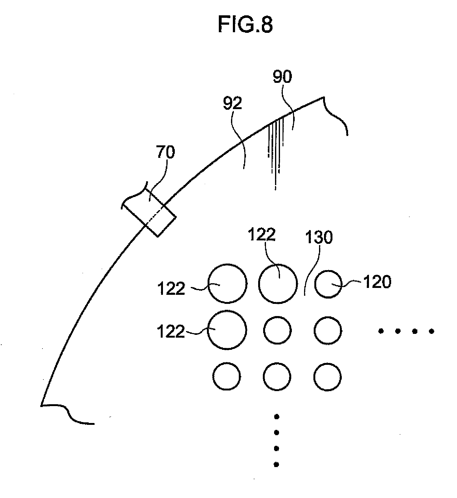
[0026] In the apparatus 1, electric current is allowed to flow from the outer circumferential section of the wafer 90 through the electrode pins 70. Therefore, plating is more easily formed in the vicinity of the electrode pins 70 than the other section, which makes it impossible to uniformly form the plating in a plane of the semiconductor wafer. This situation will be described taking a case where a post in a Wafer Level Chip Size Package (W-CSP) is formed by plating as an example.
[0027] In a W-CSP technology, connecting terminals for electrical connection between semiconductor elements formed on a semiconductor wafer and having various functions and a module substrate and the like are formed directly on the wafer in a wafer state, followed by cutting into pieces, for example with a dicing saw, to complete the package treatment. For forming the W-CSP, for example, an interlayer insulation film is formed on the semiconductor wafer with the semiconductor elements having various functions such as diodes and transistors formed thereon, rewirings connected to the semiconductor elements through via holes provided in the interlayer insulation film are formed on the interlayer insulation film, posts are formed as pillar electrodes on the rewiring, an encapsulation resin is then formed, and solder terminals are formed on the posts. Thereafter, the encapsulation resin and the semiconductor substrate are applied a dicing with a dicing blade.
[0028] In forming the posts by plating, electric current is allowed to flow from the electrode pins 70. Therefore, the posts 122 around the electrode pins 70, where electric current density is likely to be concentrated, are prone to become larger in size than the posts 120 in the other areas.
[0029] As a result, a variation in size of the posts occurs, sometimes leading to a lowered yield or the like. Even when the products are determined as a non-defective product, it is so difficult to determine with an automatic appearance identification apparatus that the products are determined as a non-defective product. Therefore, the products are determined in a manner of being reviewed by human eyes with the automatic appearance identification apparatus, disadvantageously leading to increased man-hours. Furthermore, there is a possibility that, when intending to miniaturize a post size, intervals between the posts, and distances from the posts to the wire arrangement layers in the fixture, such increased post size may pose a problem.
[0030] According to the embodiments of the present invention, in order to prevent the post size from enlarging in the product area of the wafer, the post size is intentionally enlarged in an area or areas which are not the product area. In other words, because the posts 122 facing the electrode pins 70 are enlarged, dummy posts are laid out between the electrode pins 70 and the posts 120 in the product area 130, resulting in enlargement of the dummy posts to prevent variation from occurring in the posts in the product area 130. With this, it becomes possible to suppress the variation of the post size in the product area of the semiconductor wafer 90, resulting in improved yield. In addition, a mechanical determination by the automatic appearance identification apparatus becomes available, leading to reduced man-hours. Furthermore, it is possible to prevent or suppress enlargement of a post size which is a problem in implementing miniaturization of a post size and a post pitch.
(First Embodiment)
[0031] As shown in FIG. 4, dummy post-formation areas 140 identical to the post-formation areas 121 the product area 130 in shape are disposed between the electrode pins 70 and the post-formation areas 121 of the product area 130, and plating is carried out to respectively form posts both in the post-formation areas 121 of the product area 130 and in the dummy post-formation areas 140. Although posts formed in the dummy post-formation areas 140 are enlarged, it is possible to prevent or suppress enlargement of the posts formed in the post-formation areas 121 of the product area 130.
(Second Embodiment)
[0032] When the dummy post-formation areas 140 according to the first embodiment cannot be disposed due to the distance in the layout over the whole wafer or a size of the dummy posts, rectangular dumpy post-formation areas 142 which can be disposed in a shorter distance is disposed between the electrode pins 70 and the post-formation areas 121 in the product area 130. Even in this case, the posts formed in the dummy post-formation areas 142 are also enlarged, however, it is possible to prevent or suppress enlargement of the posts formed in the post-formation areas 121 in the product area 130.
(Third Embodiment)
[0033] In the disposition of the dummy post-formation areas 140 according to the first embodiment, and of the dummy post-formation areas 142 according to the second embodiment, plural dummy post-formation areas are discretely disposed in the dummy post-formation areas 140 and the dummy post-formation areas 142, thus, there are intervals between the dummy post-formation areas 140 and between the dummy post-formation areas 142. With the intervals, a possibility, even a little, remains to influence the posts formed in the post-formation areas 121 of the product area 130.
[0034] Therefore, according to the present embodiment, the dummy post-formation areas 144 disposed between the electrode pins 70 and the post-formation areas 121 in the product area 130 are made to be in a continuous shape surrounding points where the electrode pins 70 contact, thus, it is possible to prevent enlargement of the posts formed in the post-formation areas 121 in the product area 130 by the intervals between the dummy post-formation areas. Even in this case, the posts formed in the dummy post-formation areas 144 are also enlarged, however, it is possible to prevent or suppress enlargement of the post formed in the post-formation areas 121 in the product area 130.
(Fourth Embodiment)
[0035] Even though the dummy post-formation areas 144 according to the third embodiment is made to be in a continuous shape surrounding the points where the electrode pins 70 contact, small intervals are even presented between the outermost circumferential section of the wafer and the dummy post-formation areas 144, thus even a little possibility remains to influence the posts formed in the post-formation areas 121 in the product area 130 by the plating that comes around through the intervals. Furthermore, according to the first to third embodiments, it is necessary to respectively prepare masks in order to realize the respective layouts on the wafer.
[0036] In view of the above, according to the present embodiment, a dummy post-formation area 146 disposed between the electrode pins 70 and the post-formation areas 121 in the product area 130 is made to be a shape surrounding the entire product area 130. More specifically, the dummy post-formation area 146 in an annular shape surrounding the overall product area 130 is disposed in the outer circumferential section of the wafer 90. In this way, the dummy post-formation area 146 is made to be a shape surrounding the overall product area 130, thereby always existing the dummy post-formation area 146 between the post-formation areas 121 of the product area 130 and the electrodes 70. As a result, the post formed in the dummy post-formation area 146 is enlarged, it is possible to prevent or suppress enlargement of the posts formed in the post-formation areas 121 in the product area 130 more reliably. Furthermore, predetermining the patterns of the dummy post-formation area 146 surrounding the outer circumferential section of the wafer allows a layout which can be compatible with all products, independently of a chip size and a post layout, and it has an advantage that only one mask is necessary for realizing the layout.
[0037] Although various exemplary embodiments have been shown and described, the invention is not limited to the embodiments shown. Therefore, the scope of the invention is intended to be limited solely by the scope of the claims that follow.
* * * * *
D00000
D00001
D00002
D00003
D00004
D00005
D00006
D00007
D00008
XML
uspto.report is an independent third-party trademark research tool that is not affiliated, endorsed, or sponsored by the United States Patent and Trademark Office (USPTO) or any other governmental organization. The information provided by uspto.report is based on publicly available data at the time of writing and is intended for informational purposes only.
While we strive to provide accurate and up-to-date information, we do not guarantee the accuracy, completeness, reliability, or suitability of the information displayed on this site. The use of this site is at your own risk. Any reliance you place on such information is therefore strictly at your own risk.
All official trademark data, including owner information, should be verified by visiting the official USPTO website at www.uspto.gov. This site is not intended to replace professional legal advice and should not be used as a substitute for consulting with a legal professional who is knowledgeable about trademark law.