Micro-Gap Thermal Photovoltaic Large Scale Sub-Micron Gap Method and Apparatus
Brown; Eric L. ; et al.
U.S. patent application number 13/037214 was filed with the patent office on 2011-12-29 for micro-gap thermal photovoltaic large scale sub-micron gap method and apparatus. This patent application is currently assigned to MTPV Corporation. Invention is credited to Eric L. Brown, Robert S. DiMatteo, Xiao Li, Bruno A. Nardelli, Bin Peng.
| Application Number | 20110315195 13/037214 |
| Document ID | / |
| Family ID | 45351352 |
| Filed Date | 2011-12-29 |


View All Diagrams
| United States Patent Application | 20110315195 |
| Kind Code | A1 |
| Brown; Eric L. ; et al. | December 29, 2011 |
Micro-Gap Thermal Photovoltaic Large Scale Sub-Micron Gap Method and Apparatus
Abstract
The present invention relates to micron-gap thermal photovoltaic (MTPV) technology for the solid-state conversion of heat to electricity. The problem is forming and then maintaining the close spacing between two bodies at a sub-micron gap in order to maintain enhanced performance. While it is possible to obtain the sub-micron gap spacing, the thermal effects on the hot and cold surfaces induce cupping, warping, or deformation of the elements resulting in variations in gap spacing thereby resulting in uncontrollable variances in the power output. A major aspect of the design is to allow for intimate contact of the emitter chips to the shell inside surface, so that there is good heat transfer. The photovoltaic cells are pushed outward against the emitter chips in order to press them against the inner wall. A high temperature thermal interface material improves the heat transfer between the shell inner surface and the emitter chip.
| Inventors: | Brown; Eric L.; (Cambridge, MA) ; DiMatteo; Robert S.; (Cambridge, MA) ; Nardelli; Bruno A.; (Watertown, MA) ; Peng; Bin; (Wuhan, CN) ; Li; Xiao; (Wuhan, CN) |
| Assignee: | MTPV Corporation Austin TX |
| Family ID: | 45351352 |
| Appl. No.: | 13/037214 |
| Filed: | February 28, 2011 |
Related U.S. Patent Documents
| Application Number | Filing Date | Patent Number | ||
|---|---|---|---|---|
| 61308972 | Feb 28, 2010 | |||
| Current U.S. Class: | 136/246 |
| Current CPC Class: | H01L 31/0521 20130101; Y02E 10/52 20130101; H01L 31/052 20130101; Y02E 10/50 20130101; H02S 10/30 20141201; H01L 31/024 20130101; Y02E 10/60 20130101 |
| Class at Publication: | 136/246 |
| International Class: | H01L 31/052 20060101 H01L031/052 |
Claims
1. A method for converting heat energy to electric power using sub-micron gap thermal photovoltaic technology, comprising the steps of: collecting heat energy by a collecting surface of a radiation-emitting layer from an inner surface of a thermally-conductive shell, the outer surface of the she being exposed to a high temperature heat energy source; maintaining a receiving surface of a photovoltaic cell less than one micron distance from an emitting surface of the radiation-emitting layer; receiving electromagnetic radiation by the receiving surface from the emitting surface for generating electric power by the photovoltaic cell; providing pressure on the photovoltaic cell by a pressurized, thermally conductive, deformable membrane for keeping the collecting surface of the radiation-emitting layer in close contact with the inner surface of the shell and for maximizing cooling; and providing pressure on a heat sink in contact with the thermally conductive deformable membrane for maximizing cooling.
2. The method of claim 1, further comprising creating a vacuum between the emitting surface and the receiving surface for minimizing heat conduction.
3. The method of claim 2, wherein the vacuum is less than 10.sup.-3 Torr.
4. The method of claim 1, further comprising maintaining a vacuum inside of the shell.
5. The method of claim 1 wherein the distance between the receiving surface of the photovoltaic cell and the emitting surface of the radiation-emitting layer is typically between 0.10 and 0.30 microns.
6. The method of claim 1, further comprising maintaining the distance between the receiving surface of the photovoltaic cell and the emitting surface of the radiation-emitting layer by use of thermally insulated spacers.
7. The method of claim 1, wherein the deformable membrane is pressurized by a linear actuator and a liquid metal filled cavity.
8. The method of claim 1, further comprising interposing a thermal interface between the collecting surface of a radiation-emitting layer and the inner surface of the thermally-conductive shell.
9. The method of claim 8, wherein the thermal interface comprises thermally conductive graphite.
10. The method of claim 1, further comprising reducing a temperature of the photovoltaic cell, the heat sink, the liquid metal chamber and the deformable membrane by circulating coolant liquid through heat sink cavities.
11. The method of claim 10, further comprising distributing coolant liquid through use of flexible bellows and a water distribution housing.
12. An apparatus for converting heat energy to electric power using sub-micron gap thermal photovoltaic technology, comprising: a collecting surface of a radiation-emitting layer for collecting heat energy from an inner surface of a thermally-conductive shell, the outer surface of the shell being exposed to a high temperature heat energy source; a receiving surface of a photovoltaic cell being maintained at less than one micron distance from an emitting surface of the radiation-emitting layer; electromagnetic radiation being received by the receiving surface from the emitting surface for generating electric power by the photovoltaic cell; the photovoltaic cell being pressurized by a pressurized, thermally conductive, deformable membrane for keeping the collecting surface of the radiation-emitting layer in close contact with the inner surface of the shell and for maximizing cooling; and a heat sink being pressurized to be in contact with the thermally conductive deformable membrane for maximizing cooling.
13. The apparatus of claim 12, further comprising interposing a thermal interface between the collecting surface of a radiation-emitting layer and the inner surface of the thermally-conductive shell.
14. The apparatus of claim 12, wherein the thermal interface is comprised of thermally conductive graphite.
15. The apparatus of claim 12, wherein a vacuum is maintained between the emitting surface and the receiving surface
16. The apparatus of claim 12, wherein a vacuum is maintained within the shell.
17. The apparatus of claim 12, further comprising thermally insulated spacers for maintaining the distance between the receiving surface of the photovoltaic cell and the emitting surface of the radiation-emitting layer.
18. The apparatus of claim 12, wherein the deformable membrane is pressurized by a linear actuator and a liquid metal filled cavity.
19. The apparatus of claim 12, further comprising coolant liquid distributed through use of flexible bellows and a water distribution housing.
20. An apparatus for converting heat energy to electric power using sub-micron gap thermal photovoltaic technology, comprising a shell for enclosing the components of a Quad, including: an emitter chip array maintained in close thermal contact with the shell via a graphite thermal interface; a membrane and photovoltaic array subassembly spaced apart from the emitter chip array by thermally insulated spacers; a liquid metal chamber in contact with the membrane for maintaining the emitter chip array maintained in close thermal contact with the shell; a heat sink subassembly for accepting liquid coolant for cooling the membrane, liquid metal chamber and the photovoltaic array; a water distribution housing for distributing liquid coolant to the heat sink subassembly via a bellows subassembly; a pneumatic subassembly for maintaining the heat sink in close contact with the liquid metal coolant and photovoltaic array; and a linear actuator pressure actuator for maintaining pressure in the pneumatic subassembly.
21. The apparatus of claim 20, wherein a vacuum is maintained within the shell.
22. The apparatus of claim 20, wherein the membrane is pressurized by the linear actuator and a liquid metal filled cavity.
23. The apparatus of claim 20, wherein the Quad contains a multiplicity of photovoltaic and emitter chip arrays.
24. The apparatus of claim 20, wherein a shell may an M.times.N array of Quads, where M and N are greater than or equal to one.
25. The apparatus of claim 20, further comprising a cooling control module, a vacuum control module and a pneumatic pressure control module.
Description
[0001] This application claims benefit of U.S. Provisional Application No. 61/308,972 filed on Feb. 28, 2010, and is incorporated herein by reference.
FIELD OF THE INVENTION
[0002] The present invention relates to micron-gap thermal photovoltaic (MTPV) technology for the solid-state conversion of heat to electricity. More broadly, the invention generates electrical power when it is inserted into a high temperature environment such as an industrial melting furnace.
BACKGROUND OF THE INVENTION
[0003] Thermo photovoltaic devices (TPV) consist of a heated black-body which radiates electromagnetic energy across a gap onto a photovoltaic device which converts radiant power into electrical power. The amount of power out of a given TPV device area is constrained by the temperature of the hot side of the device and generally requires very high temperatures, creating barriers to it practical use. By contrast, micron gap thermal photovoltaic (MTPV) systems allow the transfer of more power between the power emitter and receiver by reducing the size of the gap between them. By employing submicron gap technology, the achievable power density for MTPV devices can be increased by approximately an order of magnitude as compared to conventional TPV. Equivalently, for a given active area and power density, the temperature on the hot-side of an MTPV device can be reduced. This allows for new applications for on chip power, waste heat power generation and converter power.
[0004] It has been shown that electromagnetic energy transfer between a hot and cold body is a function of the close spacing of the bodies due to evanescent coupling of near fields. Thus, the closer the bodies, approximately one micron and below, the greater the power transfer. For gap spacings of 0.1 microns, increases in the rate of energy transfer of factors of five and higher are observed.
[0005] The dilemma, however, is forming and then maintaining the close spacing between two bodies at a sub-micron gap in order to maintain enhanced performance. While it is possible to obtain the sub-micron gap spacing, the thermal effects on the hot and cold surfaces induce cupping, warping, or deformation of the elements resulting in variations in gap spacing thereby resulting in uncontrollable variances in the power output.
[0006] Typically, in order to increase power output, given the lower power density of prior art devices, it has been necessary to increase the temperature. Temperature increases, however, are limited by the material of the device and system components.
[0007] Micron gap thermal photovoltaic (MTPV) systems are a potentially more efficient way to use photovoltaic cells to convert heat to electricity. Micron gap thermal photovoltaic devices are an improved method of thermal photovoltaics which is the thermal version of "solar cell" technology. Both methods make use of the ability of photons to excite electrons across the bandgap of a semi-conductor and thereby generate useful electric current. The lower the temperature of the heat source, the narrower the bandgap of the semi-conductor must be to provide the best match with the incoming spectrum of photon energy. Only those photons with energy equal to or greater than the bandgap can generate electricity. Lower energy photons can only generate heat and are a loss mechanism for efficiency. A preferred micron gap thermal photovoltaic system would include a source of heat radiated or conducted to an emitter layer which is suspended at a sub-micron gap above the surface of an infrared sensing photovoltaic cell.
[0008] By using a sub-micron gap between a hot emitting surface and a photovoltaic collector, a more enhanced rate of transfer of photons from solid to solid is observed than is possible with large gaps. Additional transfer mechanisms are involved other than simply Planck's law of the radiation, although the spectral distribution of the photons is that of a black body. The use of sub-micron gaps, however, implies that a vacuum environment is used to avoid excessive heat conduction across the gap by low energy photons that cannot excite electrons into the conduction hand. To make efficient use of the source of heat, a high fraction of high energy photons must be generated. The structure used to separate the emitting surface from the photovoltaic cell must be both small in diameter and also a very good thermal insulator for the same efficiency considerations. The photovoltaic cell will generally have to be cooled somewhat so that it will function properly. At high temperatures, intrinsic carrier generation swamps the PN junction and it is no longer an effective collector of electrons.
[0009] Micron gap thermal photovoltaic systems function as though the emitter has an emissivity value greater than one. The definition of a black body is that it has an emissivity value equal to one and this value cannot be exceeded for large gap radiant energy transfer. Equivalent emissivity factors of 5-10 have been experimentally demonstrated using gaps in the region of 0.30 to 0.10 microns.
[0010] There are at least two ways to take advantage of this phenomenon. In a comparable system, if the temperature of the emitting surfaces is kept the same, the micron gap thermal photovoltaic system can be made proportionately smaller and cheaper while producing the same amount of electricity. Or, if a comparable size system is used, the micron gap thermal photovoltaic system will run at a considerably lower temperature thereby reducing the cost of materials used in manufacturing the system. In a preliminary estimate, it was calculated that by using micron gap technology the operating temperature of a typical system could be reduced from 1,400.degree. C. to 1,000.degree. C. and still produce the same output of electricity. Such a lowering of temperature could make the difference in the practicality of the system due to the wider availability and lower cost of possible materials.
[0011] U.S. Pat. Nos. 7,390,962, 6,232,546 and 6,084,173 and U.S. patent application Ser. Nos. 12/154,120, 11/500,062, 10/895,762, 12/011,677, 12/152,196 and 12/152,195 are incorporated reference herein.
[0012] Additional energy transfer mechanisms have been postulated and the ability to build systems using narrow thermally isolated gaps may find use in many types of applications in accordance with the subject invention.
SUMMARY OF INVENTION
[0013] It is therefore an object of this invention to provide a novel micron gap thermal photovoltaic device structure which is also easier to manufacture.
[0014] It is a further object of this invention to provide such a micron gap thermal photovoltaic device which results in high thermal isolation between the emitter and the photovoltaic substrate.
[0015] It is a further object of this invention to provide such a micron gap thermal photovoltaic device which can have a large area and is capable of high yield.
[0016] It is a further object of this invention to provide such a micron gap thermal photovoltaic device which allows for lateral thermal expansion.
[0017] It is a further object of this invention to provide such a micron gap thermal photovoltaic device which is efficient.
[0018] It is a further object of this invention to provide such a micron gap thermal photovoltaic device with a uniform sub-micron gap.
[0019] It is a further object of this invention to provide such a micron gap thermal photovoltaic device which provides greater energy transfer.
[0020] It is a further object of this invention to provide such a micron gap thermal photovoltaic device which is constructed without assembling multiple discrete pieces.
[0021] It is a further object of this invention to provide a method of making a micro gap photovoltaic device.
[0022] It is a further object of this invention to provide a micron gap device useful as a thermal photovoltaic system and also useful in other applications.
[0023] The thermo photovoltaic system and apparatus generates electrical power when it is inserted into a high temperature environment, such as an industrial melting furnace. It consists of a heat and corrosion resistant, vacuum-tight shell, and a liquid-cooled mechanical assembly inside that makes contact with the inside walls of the heated shell.
[0024] The mechanical assembly facilitates and provides a means for achieving sub-micron spacing between large emitter and photovoltaic surfaces. Heat is conducted from the inner surface of the shell to a spectrally controlled radiator surface (hot side). The radiator surface emits the heat in the form of electromagnetic energy, across a sub-micron gap to a photovoltaic (PV) device (cold side). A portion of the heat is converted to electricity by the photovoltaic cell. The rest of the thermal energy is removed from the opposite side of the photovoltaic cell by a liquid cooled, pinned or finned, heat sink.
[0025] A major aspect of the design is to allow for intimate contact of the emitter chips to the shell inside surface, so that there is good heat transfer. The photovoltaic cells are pushed outward against the emitter chips in order to press them against the inner wall. A high temperature thermal interface material improves the heat transfer between the shell inner surface and the emitter chip. Tiny spacers on the emitter chips always maintain a sub-micron gap between the hot radiating surface and the photovoltaic cells.
[0026] The mechanical assembly is designed to push the hot and cold chips against the shell inside surface as the shell heats up, expands, and warps. To achieve this, the photovoltaic cells are attached to a deformable body that is able to conform to the shape of the inside surface of the shell. The deformable body is a thin metal foil (membrane). Pressure is imparted to the membrane by means of a pneumatic diaphragm and a liquid metal filled cavity.
[0027] The liquid metal cavity serves two purposes: 1) to impart pressure to the back side of the membrane, which in turn pushes the photovoltaic chips against the emitter chips, while allowing the membrane to flex and conform to the shape of the shell inside surface; and 2) to carry excess heat away from the photovoltaic to a liquid cooled heat sink.
[0028] The empty space inside the shell is a nearly perfect vacuum (<10.sup.-3 Torr), so that heat is not conducted by air across the sub-micron gap and between exposed shell inside surfaces and the heat sink.
[0029] This invention is useful because it generates electrical power from heat that otherwise would be wasted. The electricity can be used to power other devices within the plant, or it can be sold to the utility company.
[0030] The invention disclosed herein is, of course, susceptible of embodiment in many different forms. Shown in the drawings and described herein below in detail are preferred embodiments of the invention. It is to be understood, however, that the present disclosure is an exemplification of the principles of the invention and does not limit the invention to the illustrated embodiments.
BRIEF DESCRIPTION OF DRAWINGS
[0031] For a further understanding of the nature and objects of the present invention, reference should be made to the following detailed description, taken in conjunction with the accompanying drawings, in which like elements are given the same or analogous reference numbers and wherein:
[0032] FIG. 1 illustrates thermo photovoltaic and micron-gap thermo photovoltaic technology in accordance with the present invention;
[0033] FIG. 2A illustrates an embodiment of a single-sided MTPV device;
[0034] FIG. 2B illustrates an embodiment of a two-sided MTPV device;
[0035] FIG. 3 illustrates an embodiment 300 the operation of the MTPV device;
[0036] FIG. 4 illustrates a practical embodiment 400 of a cross sectional view of a front end of a "Quad" MTPV device;
[0037] FIG. 5 is a cross sectional view 500 of a Quad;
[0038] FIG. 6 illustrates a complete Quad mounted on the end of its assembly;
[0039] FIG. 7 illustrates the various parts that are assembled to form a Quad;
[0040] FIG. 8 illustrates a completely assembled Quad;
[0041] FIG. 9 illustrates a single Quad within its housing with its top cover removed;
[0042] FIG. 10 illustrates a quad module sliding into its hot housing through a furnace wall;
[0043] FIG. 11 shows a module containing four Quads and coolant connection;
[0044] FIG. 12 shows an array of Quad modules connected to common coolant lines; and
[0045] FIG. 13 shows required control modules connected to a MTPV panel comprising one or more Quads.
DETAILED DESCRIPTION OF INVENTION
[0046] Turning to FIG. 1, FIG. 1 illustrates thermo photovoltaic 104 and micron-gap thermo photovoltaic 106 technologies in accordance with the present invention. Both technologies may use heat from the combustion of gas, oil or coal 110, nuclear energy 120, waste heat from industrial processes 130 or solar heat 140. Thermo photovoltaic devices (TPV) 104 consist of a heated black-body 150 which radiates electromagnetic energy across a macro scale gap 190 onto a photovoltaic device 160 which converts radiant power into electrical power. The amount of power out of a given TPV device area is constrained by the temperature of the hot side of the device and generally requires very high temperatures, creating barriers to it practical use. By contrast, micro scale gap 195 thermal photovoltaic (MTPV) devices 106 allow the transfer of more power between the power emitter 150 and receiver 160 by reducing the size of the gap 195 between them. By employing submicron gap technology, the achievable power density for MTPV devices 106 can be increased by approximately an order of magnitude as compared to conventional TPV devices 104. Equivalently, for a given active area and power density, the temperature on the hot-side of an MTPV device can be reduced. This allows for new applications for on chip power, waste heat power generation and converter power.
[0047] It has been shown that electromagnetic energy transfer between a hot and cold body is a function of the close spacing of the bodies due to evanescent coupling of near fields. Thus, the closer the bodies 170, approximately one micron and below, the greater the power transfer. For gap spacing of 0.1 microns 180, increases in the rate of energy transfer of factors of five and higher are observed. By using a sub-micron gap 195 between a hot emitting surface 150 and a photovoltaic collector 160, a more enhanced rate of transfer of photons from solid to solid is observed than is possible with large gaps 190. Additional transfer mechanisms are involved other than simply Planck's law of the radiation, although the spectral distribution of the photons is that of a black body. The use of sub-micron gaps, however, implies that a vacuum environment is used to avoid excessive heat conduction across the gap by low energy photons that cannot excite electrons into the conduction band. To make efficient use of the source of heat, a high fraction of high energy photons must be generated. The structure used to separate the emitting surface from the photovoltaic cell must be both small in diameter and also a very good thermal insulator for the same efficiency considerations. The photovoltaic cell will generally have to be cooled somewhat so that it will function properly. At high temperatures, intrinsic carrier generation swamps the PN junction and it is no longer an effective collector of electrons.
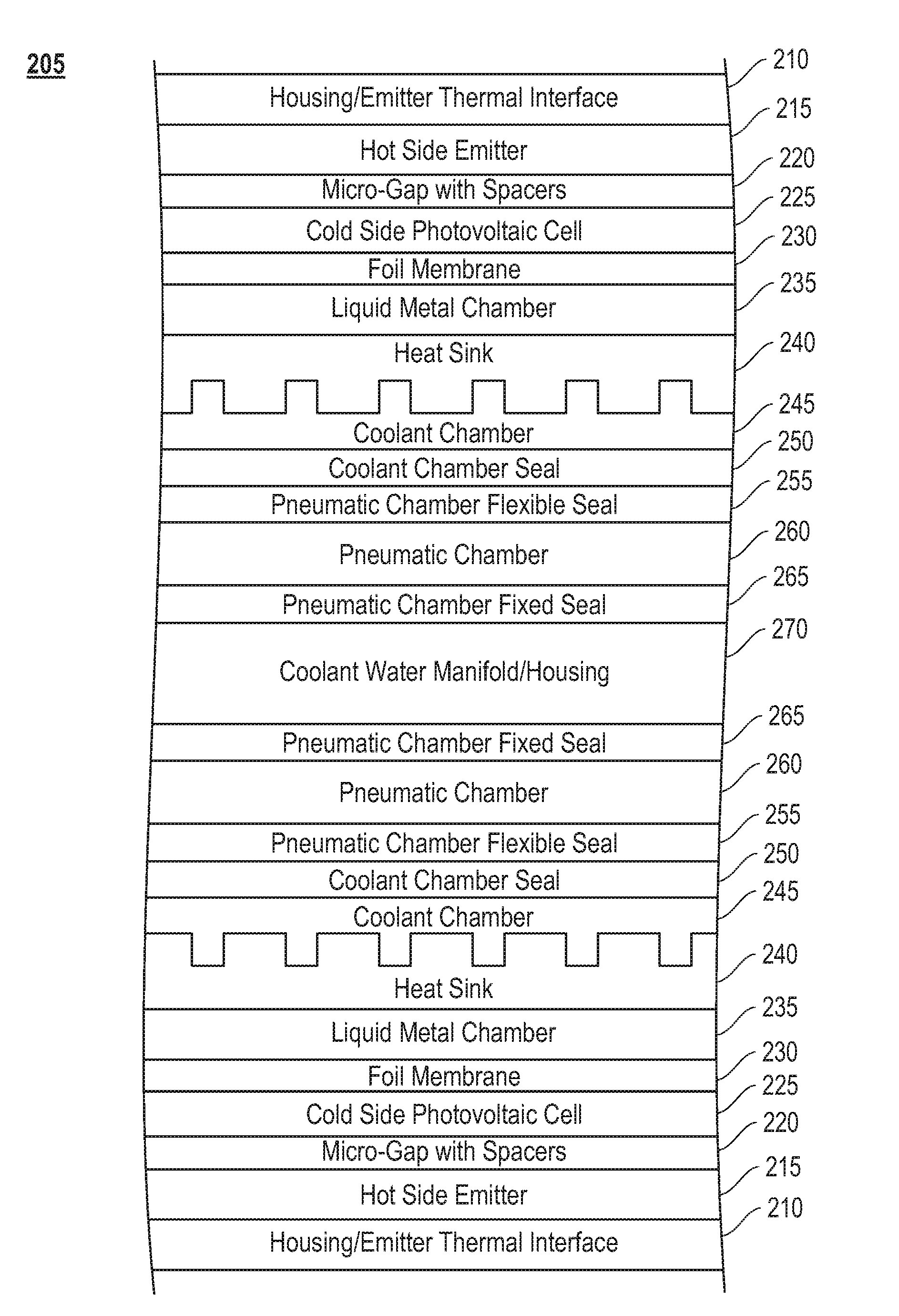
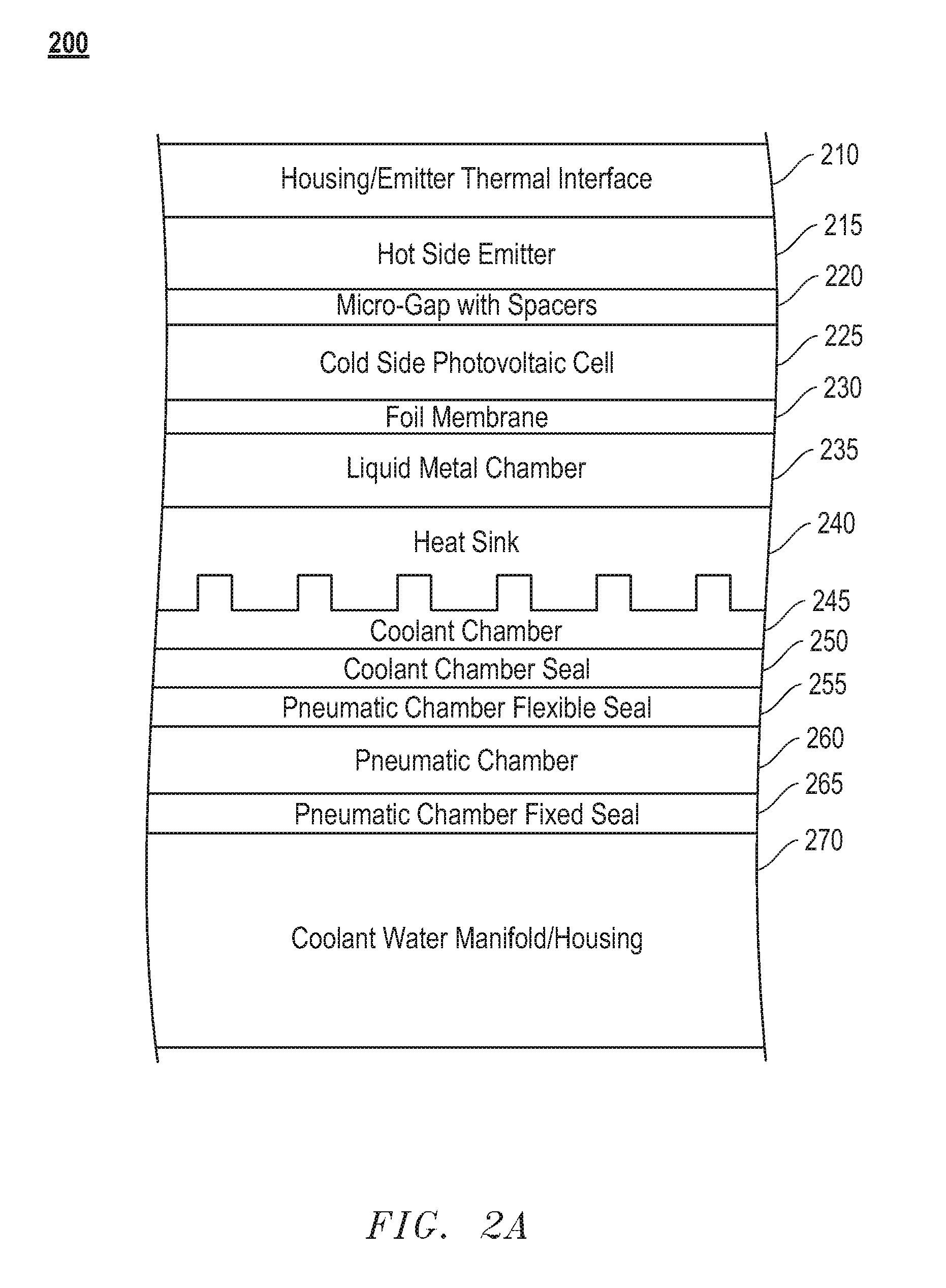
[0048] Turning to FIG. 2A, FIG. 2A illustrates an embodiment 200 of a single-sided MTPV device. The embodiment includes a thermal interface 210 for conducting heat between housing that is exposed to a high temperature and a hot side emitter 215. The hot side emitter 215 is separated from a cold side photovoltaic cell 225 by a micro-gap that is maintained by spacers 220. A foil membrane 230 is positioned between the cold side photovoltaic 225 and a chamber 235 containing a liquid metal that is maintained under controlled pressure. This pressurized chamber 235 ensures that the hot side emitter 215 and thermal interface 210 is maintained in close contact with the housing over a wide temperature range. Adjacent to the liquid metal chamber 235 is a heat sink 240 that is cooled by a continuous flow of coolant in a coolant chamber 245. The coolant chamber 245 is separated from a pneumatic chamber 260 by a coolant chamber seal 250 and a pneumatic chamber flexible seal 255. The pneumatic chamber 260 is maintained at a controlled pressure to further ensure that close contact is maintained between the heat sink 240, the liquid metal chamber 235, the cold side emitter 225, the hot side emitter 215, the thermal interface 210 and the housing. A pneumatic chamber fixed seal 265 is positioned between the pneumatic chamber 260 and a coolant water manifold 270, which is connected to a continuous supply of circulated cooling water for cooling the heat sink 240.
[0049] Turning to FIG. 2B, FIG. 2B illustrates an embodiment 205 of a two-sided MTPV device. The two-sided MTPV device includes the structure described above in relation to FIG. 2A and an additional structure that is an inverted image of that shown in FIG. 2A attached to the common coolant water manifold 270. This structure enables the collection of heat from both sides of an MTPV device.
[0050] Turning to FIG. 3, FIG. 3 illustrates an embodiment 300 that shows the operation of the MTPV device. The MTPV device 305 is exposed to radiant and convective heat flux 310, which heats the outer surface and the hot side of the hot side/cold side pair 320, 330. A vacuum is maintained in the interior of the MTPV device 305 and the cold side photovoltaic cell is cooled from the inside by circulating water 340, 350. Output power 360, 370 is obtained from the device 305.
[0051] Turning to FIG. 4, FIG. 4 illustrates a practical embodiment 400 of a cross sectional view of a front end of a "Quad" MTPV device. The Quad is a basic building block for implementing the MTPV technology. The front end includes a thermally conductive graphite interface 410 between a high temperature housing and a hot side emitter 420. A micro-gap 430 is maintained between the hot side emitter 420 and a cold side photovoltaic cell 440. A foil membrane 450 is positioned between the cold side emitter 440 and a liquid metal chamber 460. A surface of a heat sink 470 and the foil membrane 450 enclose the liquid metal chamber 460.
[0052] The purpose of the emitters 420 is to absorb heat from the inside of the housing of the Quad. An emitter chip 420 is typically, but not necessarily, made of silicon and has micro-machined silicon dioxide spacers on the gap side. The smooth side of the emitter 420 is pressed against the inside of the hot housing. A graphite thermal interface material 410 is sandwiched between the emitter 420 and the housing to improve heat transfer. The housing is heated by the radiant and convective energy within a furnace and the heat is conducted through the housing, across a thermal interface material 410 and into the silicon emitter 420, causing it to become very hot.
[0053] The photovoltaic cells 440 are designed to convert some of the light emitted from a hot body into electricity. More specifically, the photovoltaic cells 440 have a very flat surface so that when they are pressed against the spacers on the emitting surface 420, a very small vacuum gap is formed. The spacers are designed so that very little heat flow is conducted from the hot emitter 420 to the relatively cool photovoltaic cell 440. The photovoltaic cell 440 and emitter 420 are also made of high index materials to obtain a maximum amount of near-field coupled energy enhancement. A percentage of the light passing from the emitters 420 to the photovoltaic cells 440 is converted to electricity.
[0054] Turning to FIG. 5, FIG. 5 is a cross sectional view 500 of a Quad. This view is a macroscopic perspective that includes the elements shown in FIG. 4. The Quad includes a water distribution housing, also known as a coolant water manifold 510, a bellow subassembly 560, 570, a heat sink subassembly 470, a pneumatic subassembly 530, 540, 550, a liquid metal compartment 460 (see also FIG. 4), a membrane and photovoltaic subassembly 440, 450 (see also FIG. 4), hot side emitter array 410, 420 (see also FIG. 4), and a linear actuator pressure regulator (inside the water distribution housing). These elements form the basic Quad building block. One or more Quads are normally enclosed in a evacuated enclosure or hot housing that is exposed to high temperatures for generating electrical power.
[0055] The membrane 450, liquid metal 460, heat sink 470, and bellows subassemblies 570 have very coupled functionality. The metal bellows 570 transfer water between the water distribution housing 510 and the heat sink 470, one set of bellows 570 on the inlet side and the other set on the outlet side. The bellows 570 also act as expansion joints, so that when the housing heats up and expands, the bellows 570 elongate. The bellows 570 are always compressed so that they provide a force that pushes the heat sink and membrane assemblies toward the hot cover, thus pushing the photovoltaic cells 440 against the emitter spacers and pushing the emitter 420 against the hot wall. While the heat sink 470 has internal voids for water to pass through, it also acts as a suspended platform for the photovoltaic cells. Through flexing of the bellows 570, the platform can move in and out and tilt about two axes. This articulation allows the photovoltaic array 420 to conform, macroscopically, to the orientation of the hot housing. The flexible membrane 450 is there to deal with curvature of the hot housing.
[0056] The membrane 450 is a second suspension for the chips. The first suspension takes care of rigid body motions due to thermal expansion and tilt offsets due to machining tolerances and differential heating. The membrane 450 is a flexible suspension for the photovoltaic cells 440, allowing the array of cells to push against the emitters 420 and bend and flex such that the chips conform to the curved shape of the housing. It is important to note that when heat flows normal to a flat plate, there is a temperature drop across the plate which causes thermal bending, or bow. The photovoltaic cells 440 are bonded to membrane 450. The metal membrane 450 has an insulating layer and a patterned layer of electrical conductors. In this sense, the membrane 450 acts as a printed circuit board, tying the photovoltaic cells 440 together in series and/or parallel and carrying the electricity to the edge of the membrane 450.
[0057] The membrane 450 is sealed around the edges to the platform, leaving a small gap between the membrane 450 and the platform. This space is then filled with liquid metal. The liquid metal serves two purposes. First, it provides a thermal path between the photovoltaic cells 440 and the heat sink 470. Second, because it is a fluid, it allows the membrane 450 to flex.
[0058] The hot housing is made from a high temperature metal and is securely closed after the Quads are placed inside. The size of the housing depends on the number and distribution of Quads. The inside surfaces are polished so that they have a low emissivity. The outside surfaces are intentionally oxidized to a black finish so that they will absorb more radiant heat from the furnace. The housing has pass-through ports for cooling fluid, vacuum pumping, and electrical wires.
[0059] The pneumatic subassembly 530, 540, 550 sits between the water distribution housing 510 and the heat sink 470. In parallel with the bellows 570, the pneumatic diaphragm 530 pushes the heat sink 470 outward toward the hot housing, thus squeezing the photovoltaic cells 440 and emitters 420 between the membrane 450 and the hot housing. With the proper amount of pneumatic force and pressure in the liquid metal cavity, the membrane 450, chips, and housing will all take on the same shape and the gap between the emitter 420 and photovoltaic cells 440 will be uniform (but not necessarily flat).
[0060] The heat flows into the housing, through the thermal interface material 410, and into the emitter 420. It is then radiated across a sub-micron vacuum gap to the photovoltaic cell 440, where some of the energy is converted to electricity and taken away by the metallization on the membrane surface. The rest of the heat passes through the membrane 450, liquid metal, copper, copper pins, and into the cooling water, which is constantly being replenished.
[0061] If the photovoltaic cells 440 are all put in series, then bypass diodes can be connected at the ends of each row of cells, such that, if a photovoltaic cell 440 within a row were to fail, the entire row can be bypassed, and the electrical current will be passed to the next row.
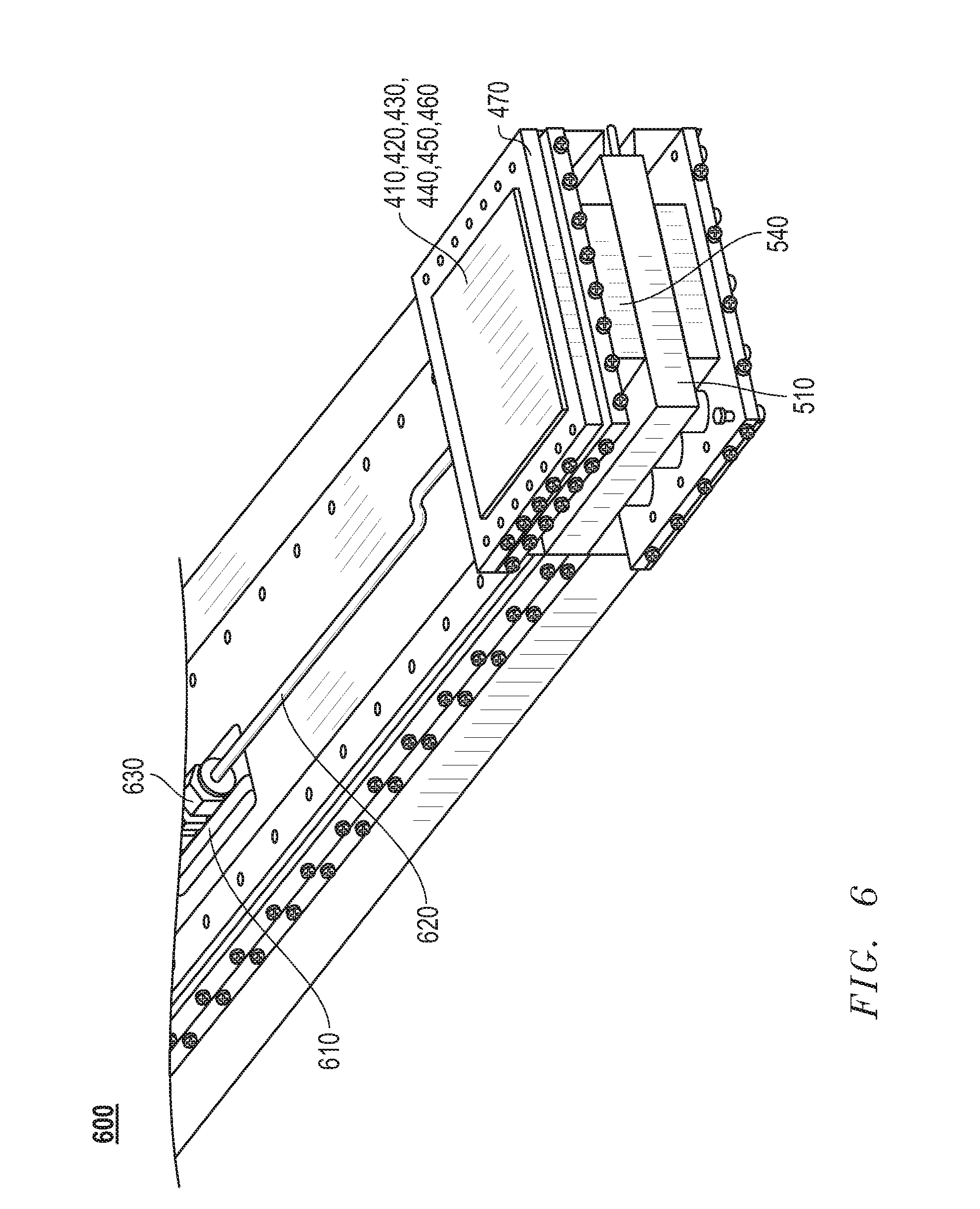
[0062] Turning to FIG. 6, FIG. 6 illustrates a complete Quad 600 mounted on the end of its assembly. Shown in FIG. 6 is a hot side emitter array 410, 420, membrane and photovoltaic assembly 440, 450, liquid metal chamber 460, heat sink 470, water distribution housing 510, pneumatic chamber 540, electrical connections 610 and pneumatic connections 620, 630.
[0063] The linear actuator consists of a motor and lead screw and is housed inside of the water distribution housing 510. Its purpose is to control the amount of liquid that is behind the membrane 450. The actuator drives a piston, which is attached to a rolling diaphragm. The interior of the diaphragm is filled with liquid metal, which can be pumped through channels that lead to the liquid metal/membrane chamber 460. To increase or decrease the amount of liquid metal behind the membrane 450, the actuator is driven outward or inward, respectively. The actuator also is used to control the pressure in the liquid metal. Between the linear actuator and the piston is a die spring. Force from the actuator goes through the spring and into the piston, so that the spring is always in compression. This allows for the actuator to modify the liquid metal pressure, even if the piston remains stationary. Compression of the die spring is directly related to the liquid metal pressure.
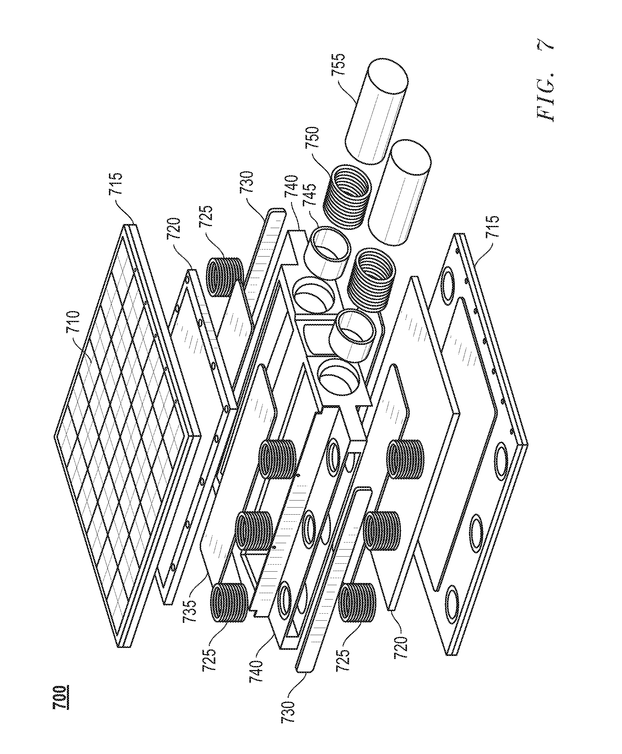
[0064] Turning to FIG. 7, FIG. 7 illustrates the various parts that are assembled to form a Quad 700. These include a photovoltaic array 710 and heat sink top 715, heat sink bottom 720, water housing top cover 735, servometer bellows 725, water housing side covers 730, water housing 740, bellows connectors 745, servometer bellows 750, and bellows tubes 755.
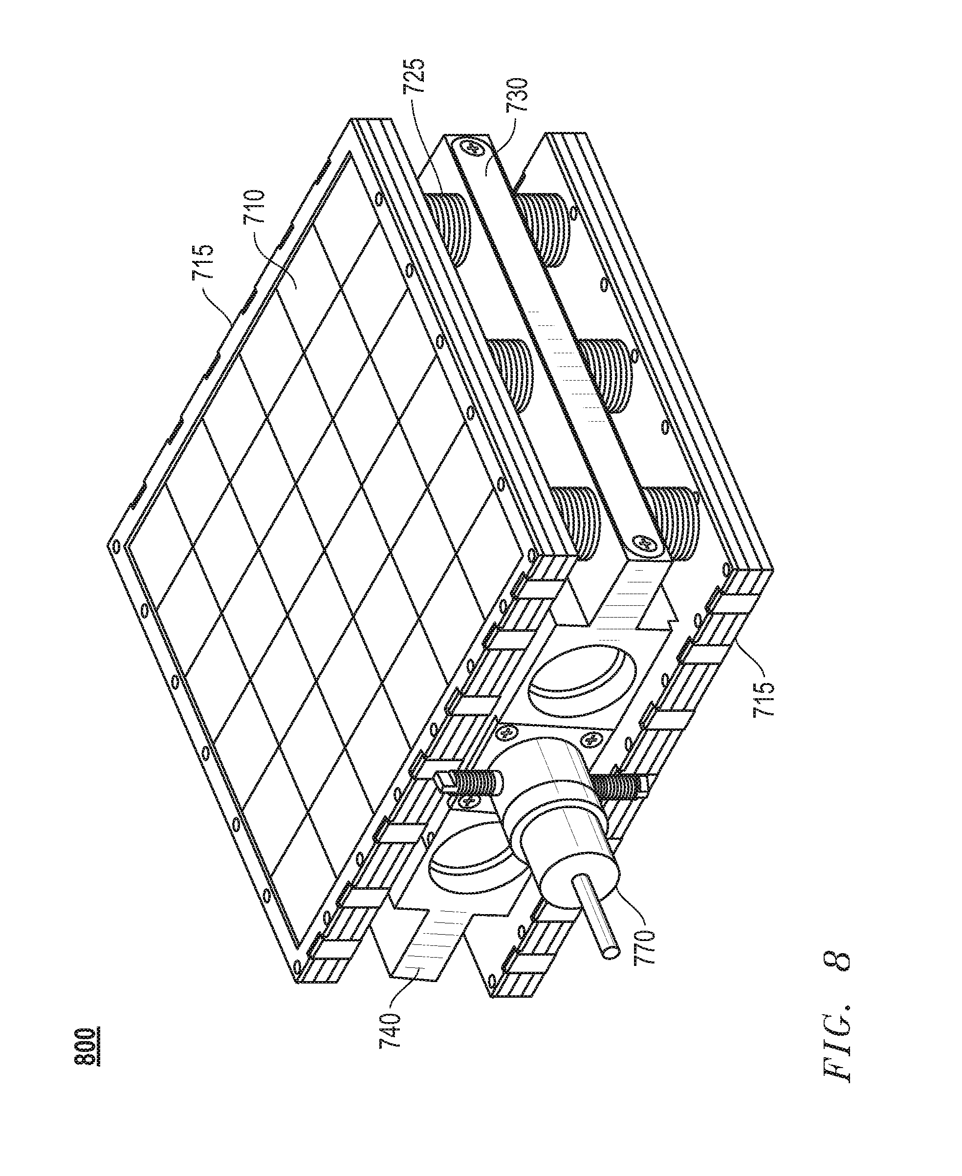
[0065] Turning to FIG. 8, FIG. 8 illustrates a completely assembled Quad 800. As shown in FIG. 8, a Quad includes a photovoltaic array 710 and heat sink top 715, servometer bellows 725, water housing side covers 730, water housing 740, and electrical and pneumatic connections 770 to external control modules.
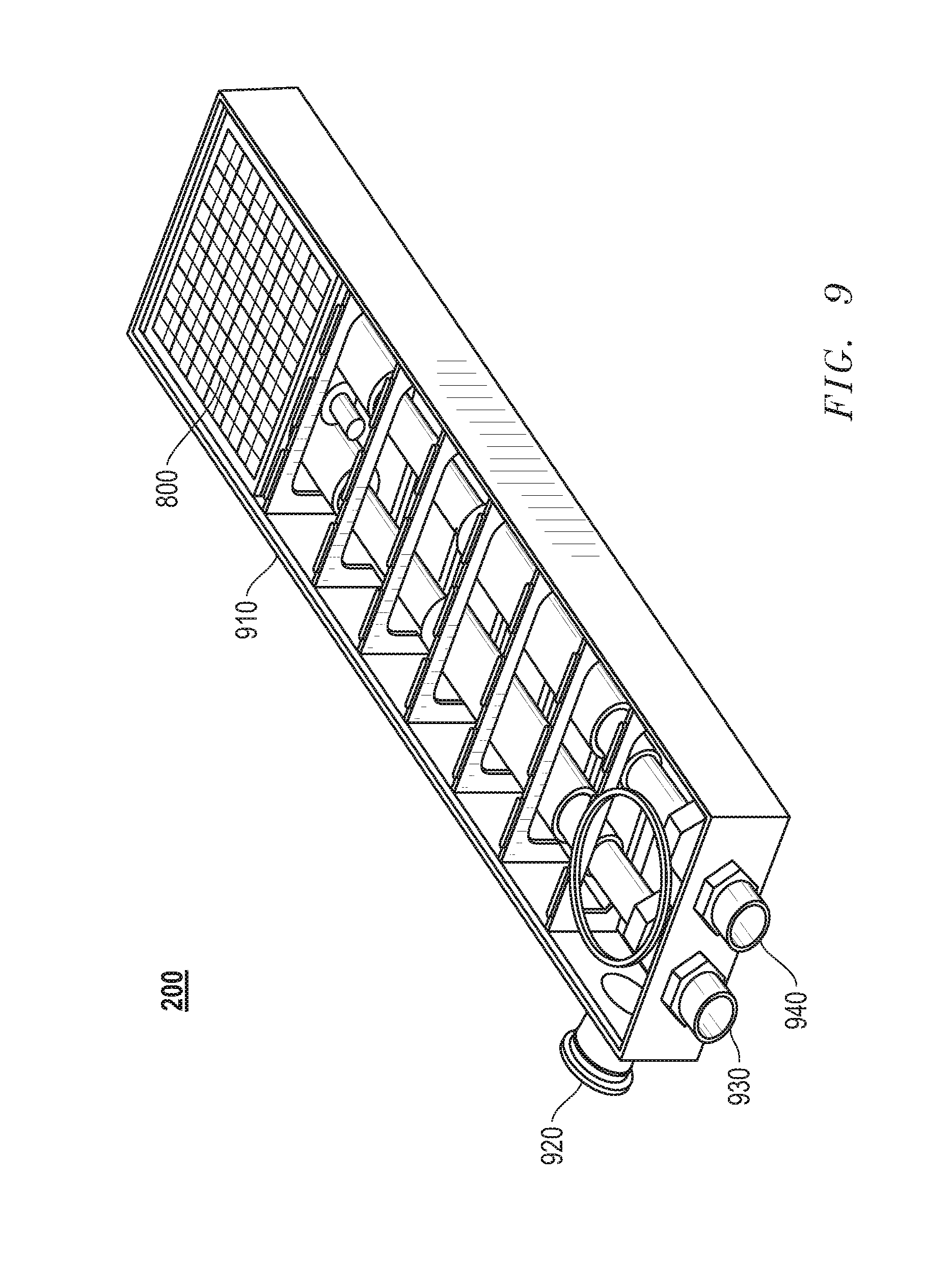
[0066] Turning to FIG. 9, FIG. 9 illustrates a single Quad 900 within its housing with its top cover removed. Shown are a complete assembled Quad 800 shown in FIG. 8, a hot housing 910, water coolant connections 930, 940 and a vacuum port 920. Not shown is a connection to a pneumatic control module.
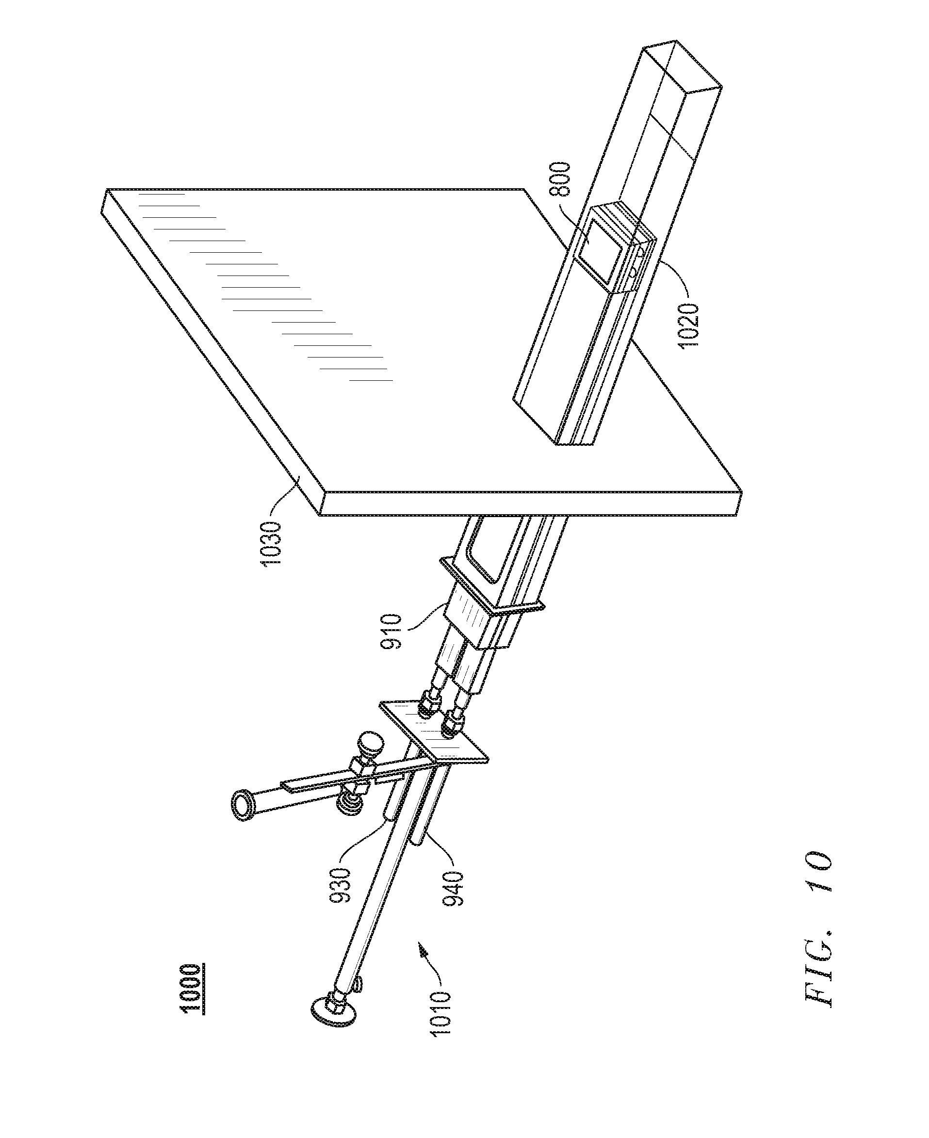
[0067] Turning to FIG. 10, FIG. 10 illustrates a quad module sliding 1000 into its hot housing through a furnace wall. Shown are a Quad 800, hot housing 1020, furnace wall 1030, a Quad module enclosure 910, water coolant connections 930, 940, and connections to electric power facilities, vacuum control module, and pneumatic control module 1010.
[0068] Turning to FIG. 11, FIG. 11 shows a module containing four Quads and coolant connection 1100. It may include up to four double-sided quad modules 800 and coolant connections 1130, 1140.
[0069] Turning to FIG. 12, FIG. 12 shows an array of Quad modules 1200 connected to common coolant lines. It shows 24 quad modules 800 connected to common coolant lines 1230, 1240. While each Quad contains arrays of photovoltaic cells and emitter chips, a panel may contain an M.times.N array of Quads, where M and N are greater than or equal to one. Quad arrays may be connected together by cooling pipes such that the units are cooled in series or parallel.
[0070] Turning to FIG. 13, FIG. 13 shows required control modules connected to a MTPV panel comprising one or more Quads 1300. Shown are a MPTV panel 1350, a cooling control module 1310, a vacuum control module 1320 and a pneumatic pressure control module 1330.
* * * * *
D00000
D00001
D00002
D00003
D00004
D00005
D00006
D00007
D00008
D00009
D00010
D00011
D00012

D00013

XML
uspto.report is an independent third-party trademark research tool that is not affiliated, endorsed, or sponsored by the United States Patent and Trademark Office (USPTO) or any other governmental organization. The information provided by uspto.report is based on publicly available data at the time of writing and is intended for informational purposes only.
While we strive to provide accurate and up-to-date information, we do not guarantee the accuracy, completeness, reliability, or suitability of the information displayed on this site. The use of this site is at your own risk. Any reliance you place on such information is therefore strictly at your own risk.
All official trademark data, including owner information, should be verified by visiting the official USPTO website at www.uspto.gov. This site is not intended to replace professional legal advice and should not be used as a substitute for consulting with a legal professional who is knowledgeable about trademark law.