Optical Logic Device
Xu; Qianfan ; et al.
U.S. patent application number 12/438720 was filed with the patent office on 2010-12-30 for optical logic device. This patent application is currently assigned to Cornell Research Foundation, Inc.. Invention is credited to Michal Lipson, Qianfan Xu.
| Application Number | 20100328744 12/438720 |
| Document ID | / |
| Family ID | 39107462 |
| Filed Date | 2010-12-30 |


| United States Patent Application | 20100328744 |
| Kind Code | A1 |
| Xu; Qianfan ; et al. | December 30, 2010 |
OPTICAL LOGIC DEVICE
Abstract
An all optical logic circuit includes a micro-ring resonator (110) optically coupled to a waveguide (115) The waveguide (115) provides multiple optical input signals (INPUT A, INPUT B) and an optical probe signal (PROBE) at a different frequency (lambda s) than the optical input signals (INPUT A, INPUT B) to the micro-ring resonator (110) such that the probe signal (PROBE) exhibits logical amplitude transitions as a function of the multiple input signals (INPUT A, INPUT B) The logical amplitude transitions of the optical probe signal (PROBE) correlate to an ANDing or NANDing of the optical input signals (INPUT A, INPUT B) In one embodiment, the all optical logic circuit is an integrated silicon device
| Inventors: | Xu; Qianfan; (Mountain View, CA) ; Lipson; Michal; (Ithaca, NY) |
| Correspondence Address: |
    SCHWEGMAN, LUNDBERG & WOESSNER, P.A.
    P.O. BOX 2938
    MINNEAPOLIS
    MN
    55402
    US
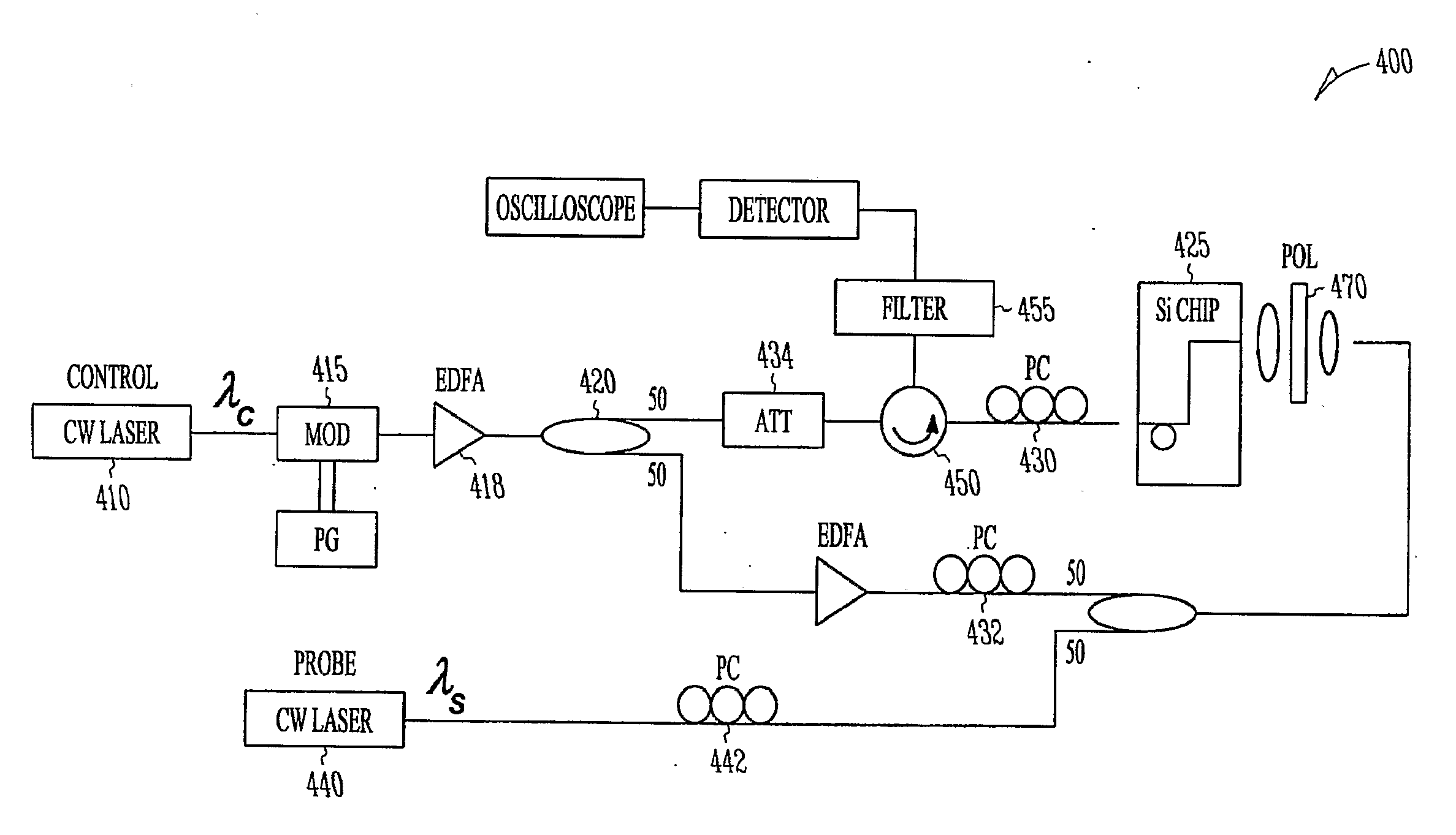
|
| Assignee: | Cornell Research Foundation,
Inc. Ithaca NY |
| Family ID: | 39107462 |
| Appl. No.: | 12/438720 |
| Filed: | August 24, 2007 |
| PCT Filed: | August 24, 2007 |
| PCT NO: | PCT/US07/18845 |
| 371 Date: | September 9, 2010 |
Related U.S. Patent Documents
| Application Number | Filing Date | Patent Number | ||
|---|---|---|---|---|
| 60839970 | Aug 24, 2006 | |||
| Current U.S. Class: | 359/108 |
| Current CPC Class: | G02F 2203/15 20130101; G02B 6/29338 20130101; G02F 3/02 20130101; G02B 6/29335 20130101 |
| Class at Publication: | 359/108 |
| International Class: | G02F 3/00 20060101 G02F003/00 |
Goverment Interests
GOVERNMENT FUNDING
[0001] This invention was made with Government support under Grant Number F49620-1-0424 awarded by Air Force Office of Scientific Research and NSF career award. The United States Government has certain rights in the invention.
Claims
1. An optical logic circuit comprising: a micro-ring resonator; and a waveguide optically coupled to the micro-ring resonator, the waveguide providing multiple optical input signals and an optical probe signal to the micro-ring resonator such that the probe signal exhibits logical amplitude transitions as a function of the multiple input signals.
2. The optical logic circuit of claim 1 wherein the logical amplitude transitions of the optical probe signal correlate to an ANDing or NANDing of the optical input signals.
3. The optical logic circuit of claim 1 wherein the all optical logic circuit comprises an integrated silicon device.
4. The optical logic circuit of claim 1 wherein the resonator has a first and a second resonance.
5. The optical logic circuit of claim 4 wherein the multiple optical input signals have frequencies at or about the first resonance and the optical probe signal has a frequency that is at approximately the second resonance.
6. The optical logic circuit of claim 5 wherein the optical input signals generate free carriers that modulate the optical probe signal.
7. The optical logic circuit of claim 6 wherein the power of the optical input signals is controlled such that a threshold for modulation is passed when the optical input signals are combined.
8. The optical logic circuit of claim 1 and further comprising a PIN junction integrated with the micro-ring resonator.
9. The optical logic circuit of claim 1 wherein the PIN junction is reverse biased.
10. An all optical logic circuit comprising: a resonator; a waveguide optically coupled to the resonator, the waveguide providing multiple optical input signals and an optical probe signal to the resonator such that the probe signal exhibits logical amplitude transitions as a function of the multiple input signals; and a filter to separate out the probe signal from the optical input signals to provide an output signal.
11. The optical logic circuit of claim 10 wherein the logical amplitude transitions of the optical probe signal correlate to an ANDing or NANDing of the optical input signals.
12. The optical logic circuit of claim 10 wherein the resonator is a micro-ring resonator having a first and a second resonance.
13. The optical logic circuit of claim 12 wherein the multiple optical input signals have frequencies at or about the first resonance and the optical probe signal has a frequency that is at approximately the second resonance.
14. The optical logic circuit of claim 13 wherein the optical input signals generate free carriers that modulate the optical probe signal.
15. The optical logic circuit of claim 14 wherein the power of the optical input signals is controlled such that a threshold for modulation is passed when the optical input signals are combined.
16. An optical logic circuit comprising: a micro-ring resonator; and means for providing multiple optical input signals and an optical probe signal to the micro-ring resonator such that the probe signal exhibits logical amplitude transitions as a function of the multiple input signals.
17. The optical logic circuit of claim 16 wherein the means for providing is at least one waveguide optically coupled to the micro-ring resonator.
18. The optical logic circuit of claim 16 wherein the means for providing further includes polarization controllers that provide signals to the resonator in a quasi-TE mode.
19. A method of forming logic gates out of optical components, the method comprising: optically coupling a resonator to a waveguide, wherein the resonator has a first and a second resonant frequency; providing two optical control signals to be logically combined to the waveguide at the first resonant frequency; providing an optical probe signal on the waveguide at the second resonant frequency, such that the optical probe is logically modulated as a function of the two optical control signals.
20. The method of claim 19 wherein the modulation of the optical probe signal correlate to an ANDing or NANDing of the optical input signals.
21. The method of claim 19 wherein the resonator has a first and a second resonance and wherein the multiple optical input signals have frequencies at or about the first resonance and the optical probe signal has a frequency that is at approximately the second resonance.
22. The method of claim 21 wherein the optical input signals generate free carriers that modulate the optical probe signal.
23. The method of claim 22 wherein the power of the optical input signals is controlled such that a threshold for modulation is passed when the optical input signals are combined.
24. The method of claim 18 and further comprising a biasing an a PIN junction integrated with the resonator to extract free carriers from the resonator.
Description
BACKGROUND
[0002] Logical devices are well known in the semiconductor arts. Various electrical circuits have been used to take one or more electrical input signals and provide an output signal that has a level representative of a logical combination of the one or more input signals. An AND logical device may be used to take two or more input signals and provide an output signal that is a logical "1" only if all of the input signals are also representative of a logical "1". A logical "1" may correspond to a high voltage, and a logical "0" may correspond to a low voltage.
[0003] There is a desire to provide such logic functions using optical signals as opposed to electrical signals. It is desired to provide such functions using compact optical devices.
BRIEF DESCRIPTION OF THE DRAWINGS
[0004] FIG. 1 is a top view of a silicon ring resonator that provides logic functions according to an example embodiment.
[0005] FIG. 2 illustrates resonant wavelengths for the ring resonator of FIG. 1.
[0006] FIG. 3 illustrates a transfer function for all-optical pulse modulation of the ring resonator of FIG. 1.
[0007] FIG. 4 is a block schematic diagram of an experimental setup for all optical logic utilizing the ring resonator of FIG. 1.
[0008] FIG. 5 illustrates waveforms of control signals and output as a logic function of a control signal according to an example embodiment.
[0009] FIG. 6 is a ring resonator with an integrated PIN junction according to an example embodiment.
[0010] FIG. 7 is a logical block diagram of an optical logic AND device according to an example embodiment.
[0011] FIG. 8 is a logical block diagram illustrating multiple NAND devices for implementing various logic devices according to an example embodiment.
DETAILED DESCRIPTION
[0012] In the following description, reference is made to the accompanying drawings that form a part hereof, and in which is shown by way of illustration specific embodiments which may be practiced. These embodiments are described in sufficient detail to enable those skilled in the art to practice the invention, and it is to be understood that other embodiments may be utilized and that structural, logical and electrical changes may be made without departing from the scope of the present invention. The following description of example embodiments is, therefore, not to be taken in a limited sense, and the scope of the present invention is defined by the appended claims.
[0013] An all-optical logic device with a micron-size silicon ring resonator utilizes a free-carrier dispersion effect in silicon. Logical AND and NAND operations may be provided at 310 Mbps with higher than 10 dB extinction ratio. A free-carrier-lifetime-limited bit-rate can be significantly improved by active carrier extraction in some embodiments.
[0014] Highly developed micro-fabrication technology enables ultra-compact optical devices integrated on silicon. All-optical logic operation is obtained using an integrated silicon device.
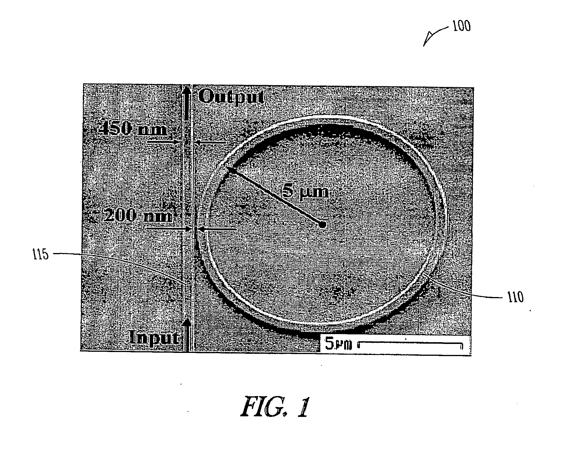
[0015] In one embodiment shown in a top view generally at 100 in FIG. 1, a silicon micro-ring resonator 110 is coupled to a straight waveguide 115. The resonator and waveguide may be fabricated on a SOI substrate using E-beam lithography, plasma dry etching, and plasma enhanced chemical vapor deposition (PECVD) for SiO2 cladding deposition. The silicon waveguides forming the resonator 110 and waveguide 115 in one embodiment have a width of approximately 450 nm and height of approximately 250 nm. The radius of the ring 110 in one embodiment is approximately R=5 .mu.m, and the spacing between the ring and the straight waveguide is approximately 150 nm. A fiber-to-fiber insertion loss for a quasi-TE mode (electric field parallel to the substrate) is measured to be 10.4 dB in one embodiment. The view of device 100 is prior to the SiO.sub.2 cladding deposition.
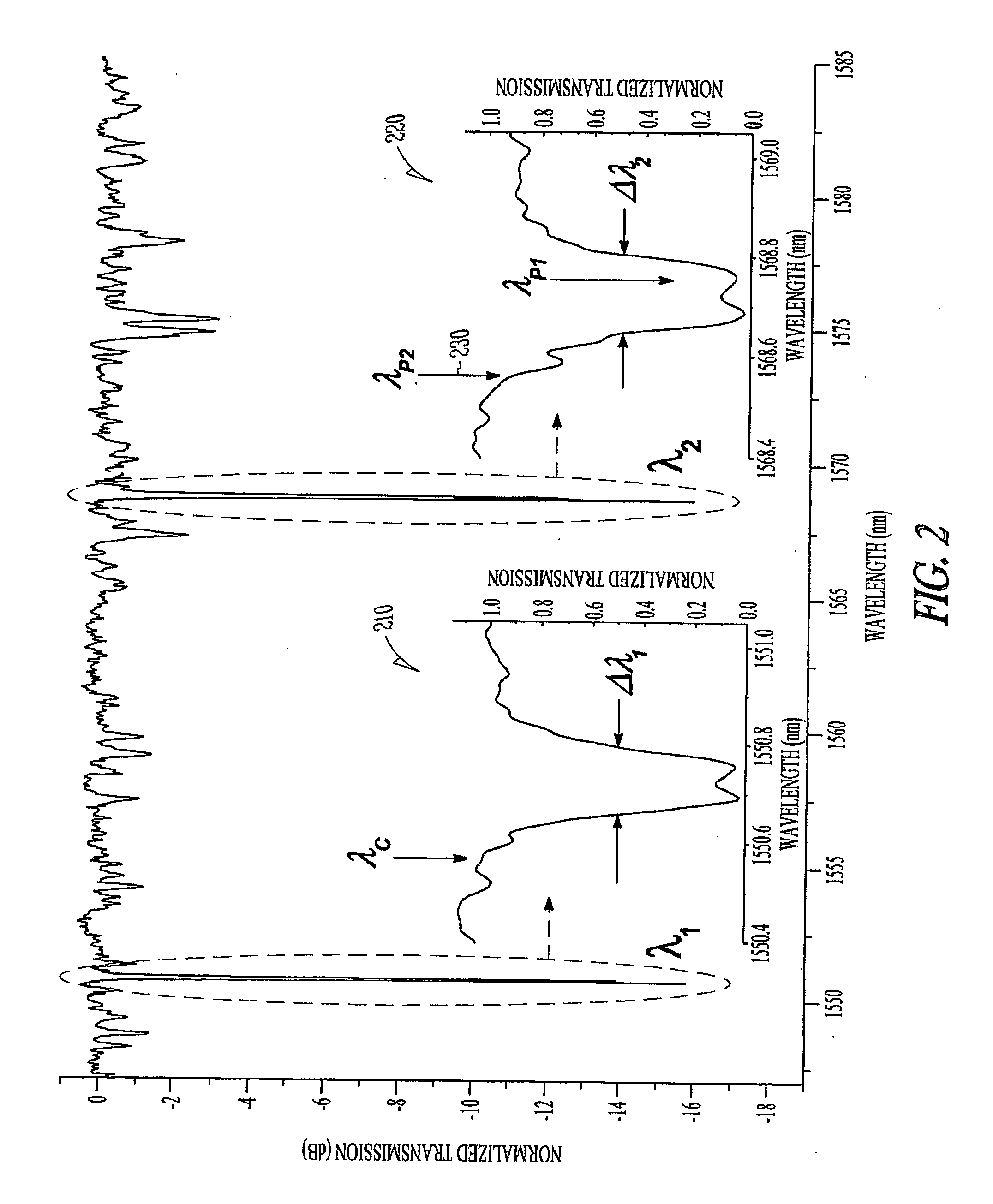
[0016] A transmission spectrum for the quasi-TE mode is shown in FIG. 2. Two resonances exist at the wavelengths .lamda.1=1550.7 nm and .lamda.2=1568.7 nm respectively. The transmission of the waveguide drops by about 16 dB at both resonances. The insets 210 and 220 of FIG. 2 show a zoom-in spectra around both resonant wavelengths. A full-width-half-maximal (FWHM) bandwidths of the resonances are approximately .DELTA..lamda.1=0.14 nm and .DELTA..lamda.2=0.16 nm, corresponding to Q1=11,076 and Q2=9,804, respectively. The wavelengths of the pump (.lamda..sub.C) and the probes for AND (.lamda..sub.P1) and NAND (.lamda..sub.P2) gates are marked in the insets.
[0017] The weak split of resonances, represented by the double-notch feature of the resonant spectrum, may be caused by a weak reflection inside the ring resonator 110. The photon lifetime of the ring resonator at .lamda.1-resonance can be obtained from Q as .tau.cav1=Q.lamda./(2.pi.c)=9.1 ps. This lifetime gives what may be a fundamental limit to the operation speed of the device. In practice, the operating speed of a fabricated device is limited by the longer carrier lifetime.
[0018] The logic operation is based on an all-optical modulation mechanism in silicon micro-ring resonator. When a strong optical control pulse or input signal and a weak cw probe light are coupled into the ring resonator through two different resonances, the control pulse generates free carriers in the ring resonator due to the two-photon absorption (TPA) effect. The generated free carriers reduce the refractive index of silicon through a plasma dispersion effect, and blue shifts the ring resonances. The probe light is therefore modulated by the resonance shift. After the control pulse leaves, the resonant wavelength and the transmission of the probe light relax back due to the fast surface recombination of the free carriers. The relaxation time is determined by the carrier lifetime of approximately 0.5 ns in the ring resonator 110.
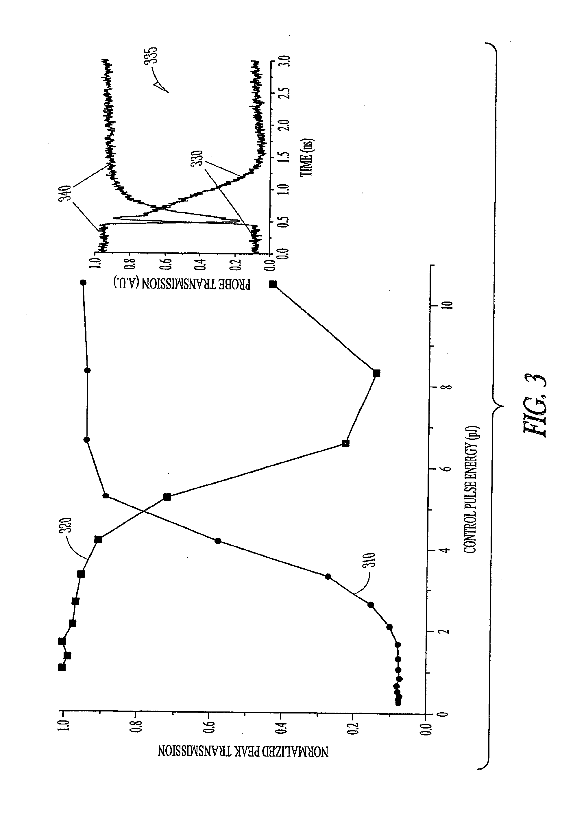
[0019] To show the relationship between the modulation depth and the energy of the control pulse, the transfer functions of the all-optical modulation process is illustrated in FIG. 3 for both the positive modulation, line 310 and negative modulation, line 320, cases, using a 14-ps long Gaussian pulse as the control pulse. A positive modulation is obtained if the wavelength of the probe light is at .lamda..sub.P1 illustrated in FIG. 2, so that the device has low transmission without the control pulse, as line 330 in the inset 335 of FIG. 3 shows. A negative modulation, shown as line 340 in the inset 335, is obtained at the probe wavelength of .lamda..sub.P2 with high transmission before the control pulse comes.
[0020] Due to the nonlinear nature of this TPA-based process, there is a clear threshold energy the control pulse has to pass to obtain large modulations. A logic-gate-like behavior is obtained on both transfer functions with a sharp transition region sandwiched between flat regions. Specifically, there is a 10-dB increase of modulation depth on the positive-modulation transfer function when the control pulse energy increased from 2.6 pJ to 5.2 pJ. Similarly, there is a 10-dB increase of modulation depth on the negative-modulation transfer function when the control pulse energy increased from 4.1 pJ to 8.2 pJ. Therefore, with properly chosen control pulse energy, dramatically different modulations may be obtained with two control pulses together compared to with only one control pulse, enabling logic operations of AND and NAND gates.
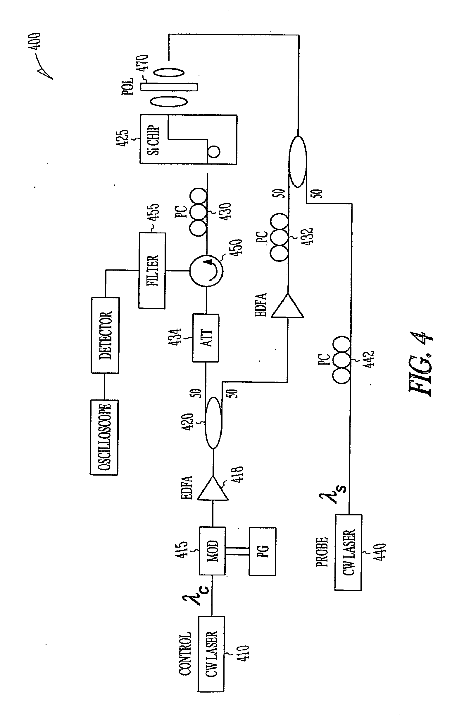
[0021] An experimental setup to demonstrate all-optical logic is shown in FIG. 4 at 400. A cw light from tunable laser 410 is modulated at 415 with a PRBS 27-1 return-to-zero (RZ) signal, which is amplified such as by an erbium-doped fiber amplifier (EDFA) 418 and split into two at splitter 420 and sent into a resonator device 425 from two opposite directions via polarization controllers (PC) 430 and 432 to avoid interference between them. One of the control signals may also be attenuated at 434. The wavelength of the control light in one embodiment is fixed at the shorter-wavelength edge of a resonance of the ring resonator, as shown by an arrow 230 in FIG. 2. A cw probe light from a laser 440 tuned at another resonance of the ring resonator, indicated at 240 in FIG. 2, is polarized at 442 and coupled together with one of the control signals at 445 and sent into the device 425. The output of the probe light is separated from the control light using an optical circulator 450 and an optical filter 455. The waveforms of the probe light are then detected at 460 and observed on an oscilloscope 465. The polarization of both control and probe light are set to be TE-like by the polarization controllers 430, 432 and 442. A polarizer 470 may also be used to provide the combined control signal and probe to the device 425.
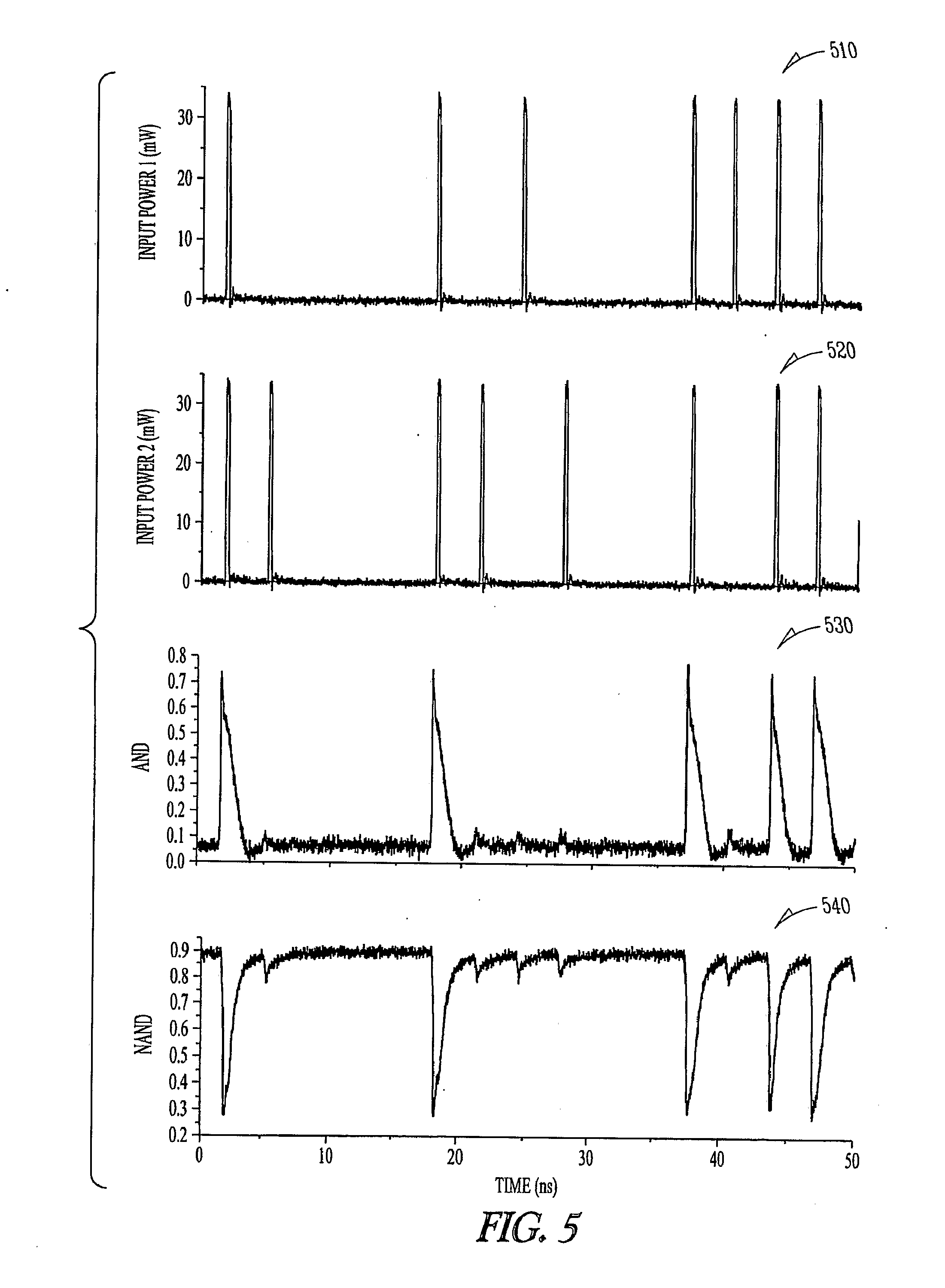
[0022] In one embodiment, the two control signals have bit-rates of 310 Mbit/s and pulse widths of 200 ps. The average optical power of each control signal is about 2 mW. The waveforms of these two control signal synchronized at the device are show at 510 and 520 in FIG. 5. When both control signal are in logic `1`, which means two control pulses are coupled into the ring resonator simultaneously, the total optical power is higher than the threshold to obtain large modulation, and a positive or negative modulation is imposed onto the probe light depending on the wavelength of the probe light. When one or both of the control signals are `0`, the total optical power is less than the threshold, and very little modulation is observed on the probe output. This results in the AND (.lamda.Probe=.lamda.P1) and NAND (.lamda.Probe=.lamda.P2) operations with extinction ration .about.10 dB, as evident from 530 and 540 respectively.
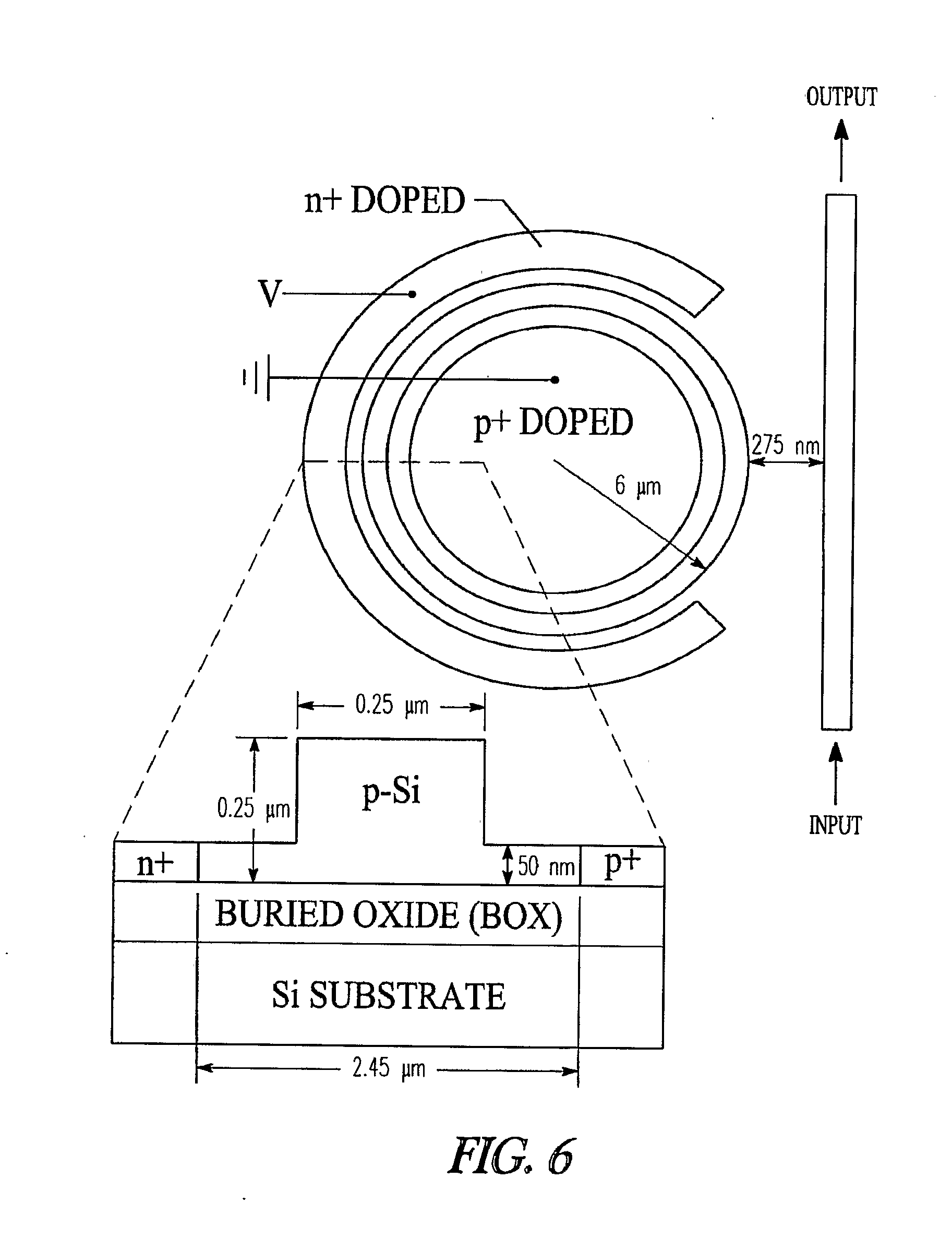
[0023] The bit-rate may be limited by the free-carrier lifetime in the resonator. In order to avoid inter-symbol interference, a second control pulse may come in after all the carriers generated by the first control pulse have recombined. To increase the speed, one can be actively extracting the carriers from the ring resonator, instead of waiting for the carriers in the ring to recombine at the Si/SiO.sub.2 interfaces. Carrier lifetime can be reduced to .about.30 ps by reversely biasing a p-i-n junction built across or integrated with the ring resonator, enabling logic operation at .about.5 Gbit/s as shown in FIG. 6.
[0024] In further embodiments, the control pulses may be generated from other logic optical devices as shown in FIG. 7 generally at an optical AND or NAND device 700. A first optical input A control signal at 710 and a second optical input B control signal at 720 may be provided to a ring resonator 730. The input signal control pulses may be provided from independent sources as opposed to a single split laser pulse in the experimental setup. A control probe 740 is also provided to the resonator 730. The control signals and probe may be provided on the same waveguide coupling to the resonator, or may be provided on separate waveguides. Similarly, an output signal 750 may be provided on a separate or same waveguide.
[0025] The power levels of the control pulses may be adjusted, and more than two control pulses or input signals may be combined to pass a threshold for logically modeling the probe signal. The term micro-ring resonator is used to describe micron or smaller ring type resonators. The size and other parameters of the ring resonators, such as refractive index may be modified to obtain different desired resonant characteristics. In further embodiments, the probe signal obtained from the resonator may be amplified and fed into further logical optical circuitry, either tuned to treat the probe signal as an input signal to be combined with other probe signals and provide yet a further probe signal output responsive to the input probe signals, or to use the probe signal as another probe signal to be modulated by further input signals. In still further embodiments, the frequency and power level of the probe output signal may be modified to that of an input signal.
[0026] A NAND gate, such as one incorporating a ring resonator as described herein, has the property of functional completeness, Any other logic function, such as a AND, OR, NOR, etc, can be implemented using NAND gates. An entire processor may be created using NAND gates. In one embodiment shown in FIG. 8 at 800, several logical devices 805, 810 and 815 may be coupled together to provide further logical functions. Each of the devices may be a NAND gate in one embodiment. Outputs from gates 805 and 810 are provided to respective optical switches 820, 825 which operate to control a pair of inputs 830, 835 to gate 815. In one embodiment, the outputs of gates 805 and 810 are amplified such as by EDFAs, and control the optical switch to modulate the input signals 830 and 835 to gate 815 at desired times. Inputs 830 and 835 may also be amplified to proper levels to function as control signals for logic gate 815. In one embodiment, the all-optical switch has the same two resonant frequencies as the NAND gate, and the output probe has a power level that is over the threshold intensity for full modulation of the input signal. If the output is high, the all-optical switch lets a new input signal pass into the next NAND gate, and if it was low, no input signal would pass (or vice versa). Several more NAND gates may be cascaded in this manner to provide a multitude of logical functions.
[0027] In various embodiments of all optical logic devices, the output of one all-optical logic device may be used as an input for a second all-optical device. The input to both all-optical logic devices has the same wavelength in one embodiment. A third all-optical logic device may be used as a converter, and the two inputs to such converter have the same wavelength as the probes and outputs of the first and second all-optical logic devices, and the wavelength of the probe and hence the output of the converter is the same as that of the input to the first and second all-optical logic devices.
[0028] In one embodiment, the coupling between the probe and the resonator of the converter is such that when the inputs to the converter are zero, the output from the converter is low or zero. In this embodiment, the output from the first all-optical logic devices provides a first input to the converter. A second input, which can be constant, at the same frequency is provided to the converter from another source such that the power of the second input alone is sufficiently below the threshold to achieve deep modulation of the converter's probe signal that little or none of the probe passes through the resonator and there is hence no output. However, when the first input is high, the sum of the first and second inputs to the converter exceeds the modulation threshold, and the probe signal passes through the resonator into the output waveguide, thereby providing an input to the second all-optical logic device at the proper input wavelength.
[0029] In another embodiment, the coupling between the probe and resonator of the converter is such that the probe signal passes through the resonator unmodulated when the inputs are zero, and the converter operates to convert a low output from the first all-optical logic devices into a high input to the second all-optical logic devices, or to convert a high output from the first all-optical logic devices into a low input to the second all-optical logic devices.
[0030] The Abstract is provided to comply with 37 C.F.R. .sctn.1.72(b) to allow the reader to quickly ascertain the nature and gist of the technical disclosure. The Abstract is submitted with the understanding that it will not be used to interpret or limit the scope or meaning of the claims.
* * * * *
D00000
D00001
D00002
D00003
D00004
D00005
D00006
D00007
D00008
XML
uspto.report is an independent third-party trademark research tool that is not affiliated, endorsed, or sponsored by the United States Patent and Trademark Office (USPTO) or any other governmental organization. The information provided by uspto.report is based on publicly available data at the time of writing and is intended for informational purposes only.
While we strive to provide accurate and up-to-date information, we do not guarantee the accuracy, completeness, reliability, or suitability of the information displayed on this site. The use of this site is at your own risk. Any reliance you place on such information is therefore strictly at your own risk.
All official trademark data, including owner information, should be verified by visiting the official USPTO website at www.uspto.gov. This site is not intended to replace professional legal advice and should not be used as a substitute for consulting with a legal professional who is knowledgeable about trademark law.