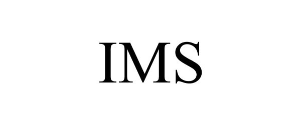
IMS
Applied Materials, Inc.
Mark For: IMS™ trademark registration is intended to cover the categories of
| Research |
|
| Serial Number | 97921174 |
| Mark Literal Elements | IMS |
| Mark Drawing Type | 4 - STANDARD CHARACTER MARK |
| Mark Type | Service Mark |
| Current Location | NEW APPLICATION PROCESSING 2023-05-08 |
| Basis | 1(b) |
| Class Status | ACTIVE |
| Primary US Classes |
|
| Primary International Class |
|
| Filed Use | No |
| Current Use | No |
| Intent To Use | Yes |
| Filed ITU | Yes |
| 44D Filed | No |
| 44E Current | No |
| 66A Current | No |
| Current Basis | No |
| No Basis | No |
| Attorney Name | Charles P. Guarino |
| Attorney Docket Number | 82399833US02 |
Timeline
| 2023-05-04 | Application Filed |
| 2023-05-08 | Location: NEW APPLICATION PROCESSING |
| 2023-05-08 | Status: Live/Pending |
| 2023-05-08 | Status: New application awaiting assignment to an examining attorney. See current trademark processing wait times for more information. |
| 2023-05-08 | Transaction Date |
Trademark Parties (Applicants & Owners)
| Party: | |
| Address | 3050 Bowers Avenue Santa Clara, CALIFORNIA UNITED STATES 95054 |
| Legal Entity Type | Corporation |
| Legal Entity State | DELAWARE |
Documents
| 2023-05-04 | ||
| 2023-05-04 |
Attorney of Record
Good, Services, and Codes
| International Codes: | 40 |
| U.S. Codes: | 100,103,106 |
| Type Code | Type |
|---|---|
| GS0401 | Treatment of materials, namely, mechanical, chemical and physical treatment of semiconductor materials substrates and silicon wafers for the manufacture of integrated chips |
Trademark Filing History
| Description | Date | Proceeding Number |
|---|---|---|
| NEW APPLICATION ENTERED | 2023-05-08 |
Similar Marks


uspto.report is an independent third-party trademark research tool that is not affiliated, endorsed, or sponsored by the United States Patent and Trademark Office (USPTO) or any other governmental organization. The information provided by uspto.report is based on publicly available data at the time of writing and is intended for informational purposes only.
While we strive to provide accurate and up-to-date information, we do not guarantee the accuracy, completeness, reliability, or suitability of the information displayed on this site. The use of this site is at your own risk. Any reliance you place on such information is therefore strictly at your own risk.
All official trademark data, including owner information, should be verified by visiting the official USPTO website at www.uspto.gov. This site is not intended to replace professional legal advice and should not be used as a substitute for consulting with a legal professional who is knowledgeable about trademark law.