TENZA
ASM IP Holding B.V.
Mark For: TENZA™ trademark registration is intended to cover the categories of
| Research |
|
| Serial Number | 97498003 |
| Mark Literal Elements | TENZA |
| Mark Drawing Type | 4 - STANDARD CHARACTER MARK |
| Mark Type | Service Mark |
| Current Location | NEW APPLICATION PROCESSING 2022-07-14 |
| Basis | 1(b) |
| Class Status | ACTIVE |
| Primary US Classes |
|
| Primary International Class |
|
| Filed Use | No |
| Current Use | No |
| Intent To Use | Yes |
| Filed ITU | Yes |
| 44D Filed | No |
| 44E Current | No |
| 66A Current | No |
| Current Basis | No |
| No Basis | No |
| Domestic Representative | Rosaleen H. Chou |
| Attorney Name | Rosaleen H. Chou |
| Attorney Docket Number | ASMINT.140TF |
Timeline
| 2022-07-11 | Application Filed |
| 2022-07-14 | Location: NEW APPLICATION PROCESSING |
| 2022-07-14 | Status: Live/Pending |
| 2022-07-14 | Status: New application will be assigned to an examining attorney approximately 6 months after filing date. |
| 2022-07-14 | Transaction Date |
Trademark Parties (Applicants & Owners)
| Party: | |
| Address | Versterkerstraat 8 Almere NETHERLANDS 1322AP |
| Legal Entity Type | Private Limited Liability Company |
| Legal Entity State | NETHERLANDS |
Documents
| 2022-07-11 | ||
| 2022-07-11 |
Attorney of Record
Good, Services, and Codes
| International Codes: | 37 |
| U.S. Codes: | 100,103,106 |
| International Codes: | 40 |
| U.S. Codes: | 100,103,106 |
| Type Code | Type |
|---|---|
| GS0371 | Manufacturing process for semiconductors; manufacturing process for integrated circuits; manufacturing process for single wafer processing tools |
Trademark Filing History
| Description | Date | Proceeding Number |
|---|---|---|
| NEW APPLICATION ENTERED IN TRAM | 2022-07-14 |
Similar Marks
Mark Image Registration | Serial | Company Trademark Application Date |
|---|---|
 TENZA 97498003 not registered Live/Pending |
ASM IP Holding B.V. 2022-07-11 |
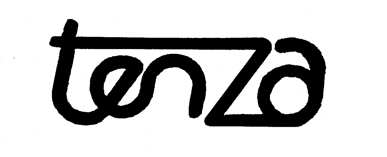
 TENZA 73617075 1434097 Dead/Cancelled |
EKTELON 1986-08-28 |
 TENZA 73548883 1382443 Dead/Cancelled |
PARADOX BY ZALO, INC. 1985-07-19 |
uspto.report is an independent third-party trademark research tool that is not affiliated, endorsed, or sponsored by the United States Patent and Trademark Office (USPTO) or any other governmental organization. The information provided by uspto.report is based on publicly available data at the time of writing and is intended for informational purposes only.
While we strive to provide accurate and up-to-date information, we do not guarantee the accuracy, completeness, reliability, or suitability of the information displayed on this site. The use of this site is at your own risk. Any reliance you place on such information is therefore strictly at your own risk.
All official trademark data, including owner information, should be verified by visiting the official USPTO website at www.uspto.gov. This site is not intended to replace professional legal advice and should not be used as a substitute for consulting with a legal professional who is knowledgeable about trademark law.