Mark For: IRM™ trademark registration is intended to cover the categories of semiconductor wafer processing equipment for the processing and production of semiconductor substrates, thin films, silicon discs and wafers; namely, epitaxial reactors, chemical vapor deposition reactors, physical vapor deposition reactors, plasma etchers, ion implanters, thin film monitoring tools, and chemical mechanical polishers. [all]
Status
2022-08-04 UTC
DEAD APPLICATION Refused Dismissed or Invalidated
This trademark application was refused, dismissed, or invalidated by the Office and this application is no longer active.
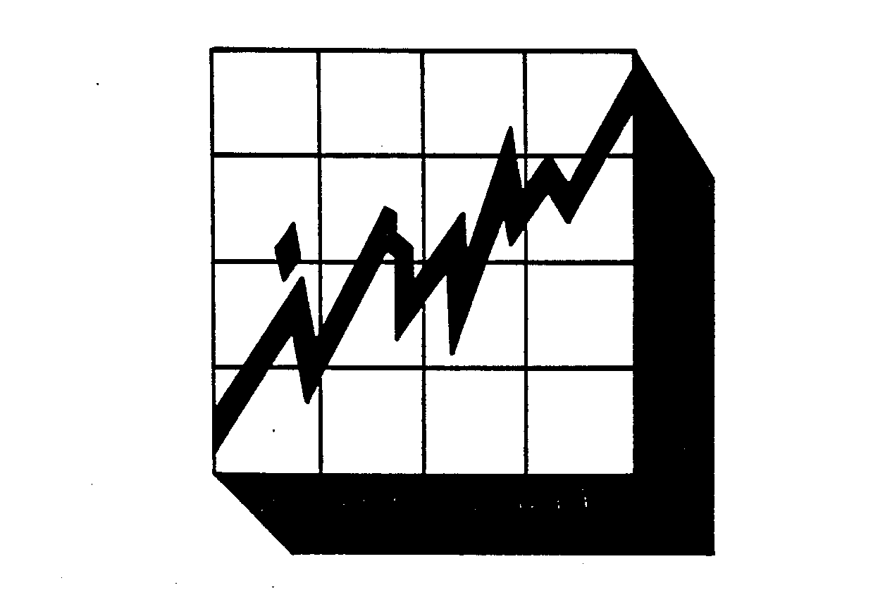
5 - AN ILLUSTRATION DRAWING WITH WORD(S) /LETTER(S)/ NUMBER(S) INSTYLIZED FORM
Mark Type
TRADEMARK
Standard Character Claim
No
Register
PRINCIPAL
Current Location
TMEG LAW OFFICE 102 - EXAMINING ATTORNEY ASSIGNED 2005-02-06
Basis
1(b)
Class Status
ACTIVE
Primary US Classes
021:
Electrical Apparatus, Machines and Supplies
023:
Cutlery, Machinery, Tools and Parts Thereof
026:
Measuring and Scientific Appliances
036:
Musical Instruments and Supplies
038:
Prints and Publications
Primary International Class
009 - Primary Class
(Electrical and scientific apparatus) Scientific, nautical, surveying, electric, photographic, cinematographic, optical, weighing, measuring, signaling, checking (supervision), lifesaving and teaching apparatus and instruments; apparatus for recording, transmission or reproduction of sound or images; magnetic data carriers, recording discs; automatic vending machines and mechanisms for coin operated apparatus; cash registers, calculating machines, data processing equipment and computers; fire-extinguishing apparatus.
Filed Use
No
Current Use
No
Intent To Use
Yes
Filed ITU
Yes
44D Filed
No
44E Current
No
66A Current
No
Current Basis
No
No Basis
No
Attorney Name
Robert W. Mulcahy
Attorney Docket Number
TM0527/ETCH/
Law Office Assigned
L20
Employee Name
SAITO, KIM TSUKIYO
Timeline
2002-01-24
Application Filed
2003-03-25
Published
2003-03-25
Published for Opposition
2004-03-21
Date of Use In Commerce
2004-03-31
Date of First Use
2005-01-04
Abandon
2005-02-06
Location: TMEG LAW OFFICE 102 - EXAMINING ATTORNEY ASSIGNED
2005-02-06
Status: Abandoned because Statement of Use failed to meet minimum filing requirements. To view all documents in this file, click on the
ROBERT W. MULCAHY APPLIED MATERIALS, INC. 2881 SCOTT BOULEVARD, M/S 2061 SANTA CLARA, CA 95054
Good, Services, and Codes
(ABANDONED) IC 009. US 021 023 026 036 038. G & S: Semiconductor wafer processing equipment for the processing and production of semiconductor substrates, thin films, silicon discs and wafers; namely, epitaxial reactors, chemical vapor deposition reactors, physical vapor deposition reactors, plasma etchers, ion implanters, thin film monitoring tools, and chemical mechanical polishers. FIRST USE: 20040331. FIRST USE IN COMMERCE: 20040321
International Codes:
9
U.S. Codes:
021,023,026,036,038
Type Code
Type
GS0091
Semiconductor wafer processing equipment for the processing and production of semiconductor substrates, thin films, silicon discs and wafers; namely, epitaxial reactors, chemical vapor deposition reactors, physical vapor deposition reactors, plasma etchers, ion implanters, thin film monitoring tools, and chemical mechanical polishers
Trademark Filing History
Description
Date
Proceeding Number
ABANDONMENT NOTICE MAILED - DEFECTIVE USE STATEMENT
uspto.report is an independent third-party trademark research tool that is not affiliated, endorsed, or sponsored by the United States Patent and Trademark Office (USPTO) or any other governmental organization. The information provided by uspto.report is based on publicly available data at the time of writing and is intended for informational purposes only.
While we strive to provide accurate and up-to-date information, we do not guarantee the accuracy, completeness, reliability, or suitability of the information displayed on this site. The use of this site is at your own risk. Any reliance you place on such information is therefore strictly at your own risk.
All official trademark data, including owner information, should be verified by visiting the official USPTO website at www.uspto.gov. This site is not intended to replace professional legal advice and should not be used as a substitute for consulting with a legal professional who is knowledgeable about trademark law.