High speed bypass cable assembly
Lloyd , et al.
U.S. patent number RE47,342 [Application Number 15/271,903] was granted by the patent office on 2019-04-09 for high speed bypass cable assembly. This patent grant is currently assigned to Molex, LLC. The grantee listed for this patent is Molex, LLC. Invention is credited to Ebrahim Abunasrah, Munawar Ahmad, Stephen W. Hamblin, Christopher David Hirschy, Eran J. Jones, Rehan Khan, Brian Keith Lloyd, Darian Ross Schulz, Gregory B. Walz, Todd David Ward.


View All Diagrams
| United States Patent | RE47,342 |
| Lloyd , et al. | April 9, 2019 |
High speed bypass cable assembly
Abstract
A cable bypass assembly is disclosed for use in providing a high speed transmission line for connecting a board mounted connector of an electronic device to a chip on the device board. The bypass cable assembly has a structure that permits it, where it is terminated to the board mounted connector and the chip member, or closely proximate thereto to replicate closely the geometry of the cable. The connector terminals are arranged in alignment with the cable signal conductors and shield extensions are provided so that shielding can be provided up to and over the termination between the cable signal conductors and the board connector terminal tails. Likewise, a similar termination structure is provided at the opposite end of the cable where a pair of terminals are supported by a second connector body and enclosed in a shield collar. The shield collar has an extension that engages the second end of the cable.
| Inventors: | Lloyd; Brian Keith (Maumelle, AR), Hirschy; Christopher David (Conway, AR), Ahmad; Munawar (Maumelle, AR), Jones; Eran J. (Conway, AR), Hamblin; Stephen W. (Little Rock, AR), Schulz; Darian Ross (Little Rock, AR), Ward; Todd David (Maumelle, AR), Walz; Gregory B. (Maumelle, AR), Abunasrah; Ebrahim (Little Rock, AR), Khan; Rehan (Little Rock, AR) | ||||||||||
|---|---|---|---|---|---|---|---|---|---|---|---|
| Applicant: |
|
||||||||||
| Assignee: | Molex, LLC (Lisle, IL) |
||||||||||
| Family ID: | 50065340 | ||||||||||
| Appl. No.: | 15/271,903 | ||||||||||
| Filed: | September 21, 2016 |
Related U.S. Patent Documents
| Application Number | Filing Date | Patent Number | Issue Date | ||
|---|---|---|---|---|---|
| PCT/US2010/022738 | Feb 1, 2010 | ||||
| 61148685 | Jan 30, 2009 | ||||
| Reissue of: | 13987296 | Feb 14, 2011 | 9011177 | Apr 21, 2015 | |
| Current U.S. Class: | 1/1 |
| Current CPC Class: | H01B 11/00 (20130101); H05K 1/0243 (20130101); H01B 11/00 (20130101); H01R 13/6593 (20130101); H01R 13/6592 (20130101); H05K 3/222 (20130101); H01R 13/6461 (20130101); H01R 13/6471 (20130101); H05K 3/222 (20130101); H05K 1/0243 (20130101); H01R 13/6593 (20130101); H01R 13/6471 (20130101); H05K 2201/10446 (20130101); H05K 2201/10674 (20130101); H05K 2201/10356 (20130101); H05K 2201/10446 (20130101); H05K 2201/10189 (20130101); H05K 2201/10189 (20130101); H05K 2201/10356 (20130101); H05K 2201/10674 (20130101) |
| Current International Class: | H01R 13/58 (20060101); H01R 13/6471 (20110101); H05K 3/22 (20060101); H05K 1/02 (20060101); H01B 11/00 (20060101); H01R 13/6593 (20110101) |
| Field of Search: | ;439/108,76.1,465,492,493,607.01,607.47,638,63,342,374,404,483,494,541.5,579,709,79,98 ;361/741 ;174/68.1,261 |
References Cited [Referenced By]
U.S. Patent Documents
| 3007131 | October 1961 | Dahlgren et al. |
| 3594613 | July 1971 | Prietula |
| 3963319 | June 1976 | Schumacher et al. |
| 4025141 | May 1977 | Thelissen |
| 4072387 | February 1978 | Sochor |
| 4083615 | April 1978 | Volinskie |
| 4157612 | June 1979 | Rainal |
| 4290664 | September 1981 | Davis et al. |
| 4307926 | December 1981 | Smith |
| 4346355 | August 1982 | Tsukii |
| 4417779 | November 1983 | Wilson |
| 4508403 | April 1985 | Weltman |
| 4611186 | September 1986 | Ziegner |
| 4615578 | October 1986 | Stadler et al. |
| 4639054 | January 1987 | Kersbergen |
| 4656441 | April 1987 | Takahashi et al. |
| 4657329 | April 1987 | Dechelette |
| 4679321 | July 1987 | Plonski |
| 4697862 | October 1987 | Hasircoglu |
| 4724409 | February 1988 | Lehman |
| 4889500 | December 1989 | Lazar et al. |
| 4924179 | May 1990 | Sherman |
| 4948379 | August 1990 | Evans |
| 4984992 | January 1991 | Beamenderfer et al. |
| 4991001 | February 1991 | Takubo et al. |
| 5112251 | May 1992 | Cesar |
| 5197893 | March 1993 | Morlion et al. |
| 5332979 | July 1994 | Roskewitsch |
| 5387130 | February 1995 | Fedder et al. |
| 5402088 | March 1995 | Pierro et al. |
| 5435757 | July 1995 | Fedder et al. |
| 5441424 | August 1995 | Morlion et al. |
| 5487673 | January 1996 | Hurtarte |
| 5509827 | April 1996 | Huppenthal et al. |
| 5554038 | September 1996 | Morlion et al. |
| 5598627 | February 1997 | Saka et al. |
| 5632634 | May 1997 | Soes |
| 5691506 | November 1997 | Miyazaki et al. |
| 5781759 | July 1998 | Kashiwabara |
| 6004139 | December 1999 | Dramstad |
| 6053770 | April 2000 | Blom |
| 6083046 | July 2000 | Wu et al. |
| 6095872 | August 2000 | Lang |
| 6144559 | November 2000 | Johnson et al. |
| 6156981 | December 2000 | Ward et al. |
| 6203376 | March 2001 | Magajne |
| 6255741 | July 2001 | Yoshihara |
| 6266712 | July 2001 | Henrichs |
| 6273753 | August 2001 | Ko |
| 6273758 | August 2001 | Lloyd et al. |
| 6366471 | April 2002 | Edwards et al. |
| 6368120 | April 2002 | Scherer |
| 6371788 | April 2002 | Bowling et al. |
| 6452789 | September 2002 | Pallotti et al. |
| 6489563 | December 2002 | Zhao et al. |
| 6535367 | March 2003 | Carpenter |
| 6574115 | June 2003 | Asano et al. |
| 6575772 | June 2003 | Soubh et al. |
| 6592401 | July 2003 | Gardner et al. |
| 6652296 | November 2003 | Kuroda et al. |
| 6652318 | November 2003 | Winings et al. |
| 6685501 | February 2004 | Wu |
| 6692262 | February 2004 | Loveless |
| 6705893 | March 2004 | Ko |
| 6780069 | August 2004 | Scherer |
| 6797891 | September 2004 | Blair et al. |
| 6824426 | November 2004 | Spink, Jr. |
| 6843657 | January 2005 | Driscoll et al. |
| 6882241 | April 2005 | Abo et al. |
| 6903934 | June 2005 | Lo |
| 6910914 | June 2005 | Spink, Jr. |
| 6916183 | July 2005 | Alger et al. |
| 6955565 | October 2005 | Lloyd et al. |
| 6969270 | November 2005 | Renfro |
| 6969280 | November 2005 | Chien |
| 6971887 | December 2005 | Trobough |
| 7004765 | February 2006 | Hsu |
| 7004793 | February 2006 | Scherer |
| 7044772 | May 2006 | McCreery |
| 7052292 | May 2006 | Hsu et al. |
| 7056128 | June 2006 | Driscoll et al. |
| 7066756 | June 2006 | Lange et al. |
| 7070446 | July 2006 | Henry |
| 7108522 | September 2006 | Verelst et al. |
| 7148428 | December 2006 | Meier et al. |
| 7168961 | January 2007 | Hsieh |
| 7175446 | February 2007 | Bright |
| 7192300 | March 2007 | Hashiguchi et al. |
| 7214097 | May 2007 | Hsu |
| 7223915 | May 2007 | Hackman |
| 7234944 | June 2007 | Nordin |
| 7244137 | July 2007 | Renfro et al. |
| 7280372 | October 2007 | Grundy et al. |
| 7307293 | December 2007 | Fjelstad |
| 7331816 | February 2008 | Krohn |
| 7384275 | June 2008 | Ngo |
| 7394665 | July 2008 | Hamasaki et al. |
| 7402048 | July 2008 | Meier et al. |
| 7431608 | October 2008 | Sakaguchi et al. |
| 7445471 | November 2008 | Scherer et al. |
| 7462924 | December 2008 | Shuey |
| 7489514 | February 2009 | Hamasaki |
| 7534142 | May 2009 | Avery |
| 7540773 | June 2009 | Ko |
| 7549897 | June 2009 | Fedder |
| 7621779 | November 2009 | Laurx et al. |
| 7637767 | December 2009 | Davis |
| 7654831 | February 2010 | Wu |
| 7658654 | February 2010 | Ohyama |
| 7690930 | April 2010 | Chen |
| 7719843 | May 2010 | Dunham |
| 7744385 | June 2010 | Scherer |
| 7744403 | June 2010 | Barr |
| 7744414 | June 2010 | Scherer et al. |
| 7748988 | July 2010 | Hori |
| 7771207 | August 2010 | Hamner et al. |
| 7789529 | September 2010 | Roberts |
| 7819675 | October 2010 | Ko et al. |
| 7824197 | November 2010 | Westman |
| 7857629 | December 2010 | Chin |
| 7857630 | December 2010 | Hermant et al. |
| 7862344 | January 2011 | Morgan et al. |
| 7892019 | February 2011 | Rao |
| 7906730 | March 2011 | Atkinson et al. |
| 7931502 | April 2011 | Iida |
| 7985097 | July 2011 | Gulla |
| 7997933 | August 2011 | Feldman |
| 8002583 | August 2011 | van Woensel |
| 8018733 | September 2011 | Jia |
| 8036500 | October 2011 | McColloch |
| 8157573 | April 2012 | Tanaka |
| 8162675 | April 2012 | Regnier |
| 8187038 | May 2012 | Kamiya |
| 8192222 | June 2012 | Kameyama |
| 8226441 | July 2012 | Regnier |
| 8308491 | November 2012 | Nichols et al. |
| 8337243 | December 2012 | Elkhatib et al. |
| 8338713 | December 2012 | Fjelstad et al. |
| 8398433 | March 2013 | Yang |
| 8419472 | April 2013 | Swanger et al. |
| 8435074 | May 2013 | Grant |
| 8439704 | May 2013 | Reed |
| 8449312 | May 2013 | Lang |
| 8449330 | May 2013 | Schroll |
| 8465302 | June 2013 | Regnier |
| 8480413 | July 2013 | Minich |
| 8517765 | August 2013 | Schroll |
| 8535069 | September 2013 | ZHang |
| 8540525 | September 2013 | Regnier |
| 8553102 | October 2013 | Yamada |
| 8575491 | November 2013 | Gundel et al. |
| 8575529 | November 2013 | Asahi |
| 8588561 | November 2013 | Zbinden |
| 8597055 | December 2013 | Regnier |
| 8651890 | February 2014 | Chiarelli |
| 8672707 | March 2014 | Nichols et al. |
| 8690604 | April 2014 | Davis |
| 8715003 | May 2014 | Buck et al. |
| 8740644 | June 2014 | Long |
| 8747158 | June 2014 | Szczesny |
| 8753145 | June 2014 | Lang |
| 8758051 | June 2014 | Nonen et al. |
| 8764483 | July 2014 | Ellison |
| 8784122 | July 2014 | Soubh |
| 8787711 | July 2014 | Zbinden |
| 8794991 | August 2014 | Ngo |
| 8804342 | August 2014 | Behziz et al. |
| 8814595 | August 2014 | Cohen et al. |
| 8834190 | September 2014 | Ngo |
| 8864521 | October 2014 | Atkinson et al. |
| 8888533 | November 2014 | Westman et al. |
| 8905767 | December 2014 | Putt, Jr. et al. |
| 8911255 | December 2014 | Scherer et al. |
| 8926342 | January 2015 | Vinther |
| 8926377 | January 2015 | Kirk |
| 8992236 | March 2015 | Wittig |
| 8992237 | March 2015 | Regnier |
| 8992258 | March 2015 | Raschilla |
| 9011177 | April 2015 | Lloyd |
| 9028281 | May 2015 | Kirk |
| 9035183 | May 2015 | Kodama et al. |
| 9040824 | May 2015 | Guetig et al. |
| 9054432 | June 2015 | Yang |
| 9071001 | June 2015 | Scherer et al. |
| 9119292 | August 2015 | Gundel |
| 9136652 | September 2015 | Ngo |
| 9142921 | September 2015 | Wanha et al. |
| 9155214 | October 2015 | Ritter |
| 9160123 | October 2015 | Pao |
| 9160151 | October 2015 | Vinther |
| 9161463 | October 2015 | Takamura |
| 9166320 | October 2015 | Herring |
| 9196983 | November 2015 | Saur et al. |
| 9203171 | December 2015 | Yu |
| 9209539 | December 2015 | Herring |
| 9214756 | December 2015 | Nishio |
| 9214768 | December 2015 | Pao |
| 9232676 | January 2016 | Sechrist et al. |
| 9246251 | January 2016 | Regnier |
| 9277649 | March 2016 | Ellison |
| 9312618 | April 2016 | Regnier |
| 9331432 | May 2016 | Phillips |
| 9350108 | May 2016 | Long |
| 9356366 | May 2016 | Moore |
| 9385455 | July 2016 | Regnier |
| 9391407 | July 2016 | Bucher |
| 9401563 | July 2016 | Simpson |
| 9413090 | August 2016 | Nagamine |
| 9413112 | August 2016 | Helster |
| 9431773 | August 2016 | Chen |
| 9437981 | September 2016 | Wu |
| 9455538 | September 2016 | Nishio |
| 9484671 | November 2016 | Zhu |
| 9484673 | November 2016 | Yang |
| 9490587 | November 2016 | Phillips |
| 9496655 | November 2016 | Huang |
| 9515429 | December 2016 | DeGeest |
| 9525245 | December 2016 | Regnier |
| 9543688 | January 2017 | Pao |
| 9553381 | January 2017 | Regnier |
| 9559465 | January 2017 | Phillips |
| 9565780 | February 2017 | Nishio |
| 9608388 | March 2017 | Kondo |
| 9608590 | March 2017 | Hamner |
| 9627818 | April 2017 | Chen |
| 9660364 | May 2017 | Wig et al. |
| 9666998 | May 2017 | deBoer |
| 9673570 | June 2017 | Briant |
| 9812799 | November 2017 | Wittig |
| 9985367 | May 2018 | Wanha et al. |
| 2001/0016438 | August 2001 | Reed |
| 2002/0111067 | August 2002 | Sakurai et al. |
| 2002/0157865 | October 2002 | Noda |
| 2002/0180554 | December 2002 | Clark et al. |
| 2003/0064616 | April 2003 | Reed et al. |
| 2003/0073331 | April 2003 | Peloza |
| 2003/0222282 | December 2003 | Fjelstad et al. |
| 2004/0029406 | February 2004 | Loveless |
| 2004/0094328 | May 2004 | Fjelstad et al. |
| 2004/0121633 | June 2004 | David |
| 2004/0155328 | August 2004 | Kline |
| 2004/0155734 | August 2004 | Kosemura et al. |
| 2004/0229510 | November 2004 | Lloyd et al. |
| 2004/0264894 | December 2004 | Cooke |
| 2005/0006126 | January 2005 | Aisenbrey |
| 2005/0051810 | March 2005 | Funakura |
| 2005/0093127 | May 2005 | Fjelstad et al. |
| 2005/0130490 | June 2005 | Rose |
| 2005/0142944 | June 2005 | Ling |
| 2005/0239339 | October 2005 | Pepe |
| 2006/0001163 | January 2006 | Kolbehdari et al. |
| 2006/0035523 | February 2006 | Kuroda et al. |
| 2006/0038287 | February 2006 | Hamasaki |
| 2006/0067066 | March 2006 | Meier |
| 2006/0079102 | April 2006 | DeLessert |
| 2006/0079119 | April 2006 | Wu |
| 2006/0091507 | May 2006 | Fjelstad et al. |
| 2006/0114016 | June 2006 | Suzuki |
| 2006/0160399 | July 2006 | Dawiedczyk |
| 2006/0189212 | August 2006 | Avery |
| 2006/0194475 | August 2006 | Miyazaki |
| 2006/0216969 | September 2006 | Bright |
| 2006/0228922 | October 2006 | Morriss |
| 2006/0234556 | October 2006 | Wu |
| 2006/0238991 | October 2006 | Drako |
| 2006/0282724 | December 2006 | Roulo |
| 2006/0292898 | December 2006 | Meredith |
| 2007/0032104 | February 2007 | Yamada |
| 2007/0141871 | June 2007 | Scherer |
| 2007/0243741 | October 2007 | Yang |
| 2008/0131997 | June 2008 | Kim et al. |
| 2008/0171476 | July 2008 | Liu |
| 2008/0297988 | December 2008 | Chau |
| 2008/0305689 | December 2008 | Zhang |
| 2009/0023330 | January 2009 | Stoner et al. |
| 2009/0166082 | July 2009 | Liu et al. |
| 2009/0215309 | August 2009 | Mongold |
| 2010/0068944 | March 2010 | Scherer |
| 2010/0112850 | May 2010 | Rao |
| 2010/0159829 | June 2010 | McCormack |
| 2010/0177489 | July 2010 | Yagisawa |
| 2010/0203768 | August 2010 | Kondo |
| 2011/0074213 | March 2011 | Schaffer |
| 2011/0080719 | April 2011 | Jia |
| 2011/0136387 | June 2011 | Matsuura |
| 2011/0212633 | September 2011 | Regnier |
| 2011/0230104 | September 2011 | Lang |
| 2011/0263156 | October 2011 | Ko |
| 2011/0300757 | December 2011 | Regnier |
| 2011/0304966 | December 2011 | Schrempp |
| 2012/0003848 | January 2012 | Casher |
| 2012/0034820 | February 2012 | Lang |
| 2012/0225585 | September 2012 | Lee |
| 2012/0246373 | September 2012 | Chang |
| 2013/0005178 | January 2013 | Straka et al. |
| 2013/0012038 | January 2013 | Kirk |
| 2013/0017715 | January 2013 | Laarhoven |
| 2013/0040482 | February 2013 | Ngo |
| 2013/0092429 | April 2013 | Ellison |
| 2013/0148321 | June 2013 | Liang |
| 2013/0340251 | December 2013 | Regnier |
| 2014/0041937 | February 2014 | Lloyd et al. |
| 2014/0073173 | March 2014 | Yang |
| 2014/0073174 | March 2014 | Yang |
| 2014/0073181 | March 2014 | Yang |
| 2014/0111293 | April 2014 | Madeberg et al. |
| 2014/0217571 | August 2014 | Ganesan et al. |
| 2014/0242844 | August 2014 | Wanha |
| 2014/0273551 | September 2014 | Resendez |
| 2014/0273594 | September 2014 | Jones et al. |
| 2014/0335736 | November 2014 | Regnier |
| 2015/0079845 | March 2015 | Wanha |
| 2015/0090491 | April 2015 | Dunwoody |
| 2015/0180578 | June 2015 | Leigh et al. |
| 2015/0207247 | September 2015 | Chen et al. |
| 2016/0013596 | January 2016 | Regnier |
| 2016/0064119 | March 2016 | Grant |
| 2016/0104956 | April 2016 | Santos |
| 2016/0181713 | June 2016 | Peloza |
| 2016/0190720 | June 2016 | Lindkamp |
| 2016/0190747 | June 2016 | Regnier |
| 2016/0197423 | July 2016 | Regnier |
| 2016/0218455 | July 2016 | Sayre |
| 2016/0233598 | August 2016 | Wittig |
| 2016/0233615 | August 2016 | Scholeno |
| 2016/0336692 | November 2016 | Champion |
| 2016/0380383 | December 2016 | Lord |
| 2017/0033482 | February 2017 | Liao |
| 2017/0033509 | February 2017 | Liao |
| 2017/0077621 | March 2017 | Liao |
| 2017/0098901 | April 2017 | Regnier |
| 2017/0110222 | April 2017 | Liptak et al. |
| 2017/0162960 | June 2017 | Wanha |
| 2017/0302036 | October 2017 | Regnier |
| 2017/0365942 | December 2017 | Regnier |
| 2018/0034175 | February 2018 | Lloyd |
| 3447556 | Jul 1986 | DE | |||
| 3447556 | Oct 1986 | DE | |||
| 02-079571 | Jun 1990 | JP | |||
| 04-14372 | Feb 1992 | JP | |||
| 05-059761 | Aug 1993 | JP | |||
| 2008-041285 | Feb 2008 | JP | |||
| 2008-059857 | Mar 2008 | JP | |||
| 2009-043590 | Feb 2009 | JP | |||
| 2010-017388 | Jan 2010 | JP | |||
| 2010-123274 | Jun 2010 | JP | |||
| 2013-016394 | Jan 2013 | JP | |||
| M359141 | Jun 2009 | TW | |||
| M408835 | Aug 2011 | TW | |||
| 201225455 | Jun 2012 | TW | |||
| WO 2008-072322 | Jun 2008 | WO | |||
| WO 2012-078434 | Jun 2012 | WO | |||
| WO 2013-006592 | Jan 2013 | WO | |||
Other References
|
US. Appl. No. 61/714,871, filed Oct. 17, 2012, Wig et al. cited by applicant . Agilent, "Designing Scalable 10G Backplane Interconnect Systems Utilizing Advanced Verification Methodologies," White Paper, Published May 5, 2012, USA. cited by applicant . Amphenol Aerospace, "Size 8 High Speed Quadrax and Differential Twinax Contacts for Use in MIL-DTL-38999 Special Subminiature Cylindrical and ARINC 600 Rectangular Connectors", published May 2008. Retrieved from www.peigenesis.com/images/content/news/amphenol_quadrax.pdf. cited by applicant . Hitachi Cable America Inc., "Direct Attach Cables: OMNIBIT supports 25 Gbit/s interconnections". Retrieved Aug. 10, 2017 from www.hca.hitachi-cable.com/products/hca/catalog/pdfs/direct-attach-cable-a- ssemblies.pdf. cited by applicant . Amphenol TCS, "Amphenol TCS expands the XCede Platform with 85 Ohm Connectors and High-Speed Cable Solutions," Press Release, Published Feb. 25, 2009, http://www.amphenol.com/about/news_archive/2009/58. cited by applicant . "File:Wrt54gl-layout.jpg-Embedded Xinu", Internet Citation, Sep. 8, 2006. Retrieved from the Internet: URL:http://xinu.mscs.edu/File:Wrt54gl-layout.jpg [retrieved on Sep. 23, 2014]. cited by applicant. |
Primary Examiner: Lee; Christopher E.
Attorney, Agent or Firm: Molex, LLC
Parent Case Text
.Iadd.This is a reissue application of U.S. Pat. No. 9,011,177, Issued Apr. 21, 2015. .Iaddend.
REFERENCE To RELATED APPLICATIONS
The Present Disclosure is a continuation-in-part of International Application No. PCT/US2010/022738, filed Feb. 1, 2010, entitled "High Speed Interconnect Cable Assembly," filed 01 Feb. 2010 with the U.S. Patent And Trademark Office (USPTO) as Receiving Office for the Patent Cooperation Treaty. The '738 Application claims priority of prior-filed U.S. Provisional Application No. 61/145,685, entitled "High Speed Interconnect Cable Assembly," filed 30 Jan. 2009 also with the USPTO. The contents of each of the above Applications are fully incorporated in their entireties herein.
Claims
What is claimed is:
1. A cable bypass assembly, the cable bypass assembly comprising: a first connector, the first connector being configured for mounting to a circuit board, the first connector including a connector body, the connector body .Iadd.including a card slot and .Iaddend.supporting a plurality of conductive terminals .Iadd.that extend into the card slot.Iaddend., the conductive terminals including contact portions and tail portions, the contact portions being held within the .[.connector body.]. .Iadd.card slot .Iaddend.for contacting a mating blade of an opposing, mating connector, the tail portions extending .[.out from the connector body.]. .Iadd.rearward of the card slot.Iaddend.; an elongated cable, the elongated cable including: a pair of signal conductors, the signal conductors being disposed within an insulative body portion of the elongated cable, the signal conductors extending, in a spaced-apart relationship, lengthwise through a body portion of the elongated cable, a conductive shield, the conductive shield extending over an exterior of the elongated cable body portion, an insulative outer covering, the insulative outer covering extending over the conductive shield, and opposing first and second free ends, the first free end terminating directly to selected terminal tails of the first connector in a manner so that the signal conductors are in electrical communication with a pair of signal terminal tails; a shield extension member, the shield extension member being configured to engage a first length of the conductive shield exposed at the first free end and extending therefrom over the signal conductors attached to the pair of signal terminal tails, the shield extension member including at least two spaced apart mounting feet; and a second connector, the second connector including: an insulative body, the insulative body supporting at least a pair of conductive signal terminals in a spaced-apart relationship, each conductive signal terminal including contact and tail portions .Iadd.wherein the second free end is connected to the tail portions of the at least a pair of terminals in the insulative body.Iaddend., and a shielding collar, the shielding collar enclosing a body portion of the second connector, the shielding collar includes an extension portion, the extension portion engaging and receiving the conductive shield exposed at the second free end.Iadd.; wherein the cable bypass assembly is configured to support 10 GHz signaling.Iaddend..
2. The cable bypass assembly of claim 1, further including a second cable, the second cable including a pair of signal conductors, the second cable signal conductors disposed lengthwise therethrough in a spaced-apart relationship, the second cable signal conductors being attached to corresponding signal terminal tails of the first connector alongside the elongated cable.
3. The cable bypass assembly of claim 1, wherein the shield extension member further includes a cup portion, the cup portion being configured to receive the first free end therein.
4. The cable bypass assembly of claim 2, wherein the shield extension member further includes a pair of cup portions, each cup portion .[.receivings.]. .Iadd.receiving .Iaddend.ends of the two cables therein.
5. The cable bypass assembly of claim 4, wherein the shield extension member includes at least three mounting feet, two of the mounting feet being disposed on opposing side edges of the shield extension member and a third of the three mounting feet being disposed between the cup portions.
6. The cable bypass assembly of claim 5, wherein the mounting feet and the two cable signal conductors are aligned with each other.
7. The cable bypass assembly of claim 1, wherein the tail and contact portions extend uninterruptedly lengthwise in a general horizontal plane through the .[.first.]. connector body.
8. The cable bypass assembly of claim 1, wherein the elongated cable includes a preselected length of flexible circuitry.
9. .[.The cable bypass assembly of claim 1,.]. .Iadd.A cable bypass assembly, the cable bypass assembly comprising: a first connector, the first connector being configured for mounting to a circuit board, the first connector including a connector body, the connector body including a card slot and supporting a plurality of conductive terminals that extend into the card slot, the conductive terminals including contact portions and tail portions, the contact portions being held within the card slot for contacting a mating blade of an opposing, mating connector, the tail portions extending rearward of the card slot; an elongated cable, the elongated cable including: a pair of signal conductors, the signal conductors being disposed within an insulative body portion of the elongated cable, the signal conductors extending, in a spaced-apart relationship, lengthwise through a body portion of the elongated cable, a conductive shield, the conductive shield extending over an exterior of the elongated cable body portion, an insulative outer covering, the insulative outer covering extending over the conductive shield, and opposing first and second free ends, the first free end terminating directly to selected terminal tails of the first connector in a manner so that the signal conductors are in electrical communication with a pair of signal terminal tails; a shield extension member, the shield extension member being configured to engage a first length of the conductive shield exposed at the first free end and extending therefrom over the signal conductors attached to the pair of signal terminal tails, the shield extension member including at least two spaced apart mounting feet; and a second connector, the second connector including: an insulative body, the insulative body supporting at least a pair of conductive signal terminals in a spaced-apart relationship, each conductive signal terminal including contact and tail portions wherein the second free end is connected to the tail portions of the at least a pair of terminals in the insulative body, and a shielding collar, the shielding collar enclosing a body portion of the second connector, the shielding collar includes an extension portion, the extension portion engaging and receiving the conductive shield exposed at the second free end, .Iaddend.wherein the shielding collar further includes at least one through-hole terminal, the through-hole terminal extending from the shielding collar and engaging a through-hole of the circuit board.
10. The cable bypass assembly of claim 1, wherein the shielding collar further includes a cap portion, the cap portion having a cup portion formed therein, the cup portion being configured to receive an exposed second end of the cable therein and contact a length of exposed cable shielding.
11. .[.The cable bypass assembly of claim 1,.]. .Iadd.A cable bypass assembly, the cable bypass assembly comprising: a first connector, the first connector being configured for mounting to a circuit board, the first connector including a connector body, the connector body including a card slot and supporting a plurality of conductive terminals that extend into the card slot, the conductive terminals including contact portions and tail portions, the contact portions being held within the card slot for contacting a mating blade of an opposing, mating connector, the tail portions extending rearward of the card slot; an elongated cable, the elongated cable including: a pair of signal conductors, the signal conductors being disposed within an insulative body portion of the elongated cable, the signal conductors extending, in a spaced-apart relationship, lengthwise through a body portion of the elongated cable, a conductive shield, the conductive shield extending over an exterior of the elongated cable body portion, an insulative outer covering, the insulative outer covering extending over the conductive shield, and opposing first and second free ends, the first free end terminating directly to selected terminal tails of the first connector in a manner so that the signal conductors are in electrical communication with a pair of signal terminal tails; a shield extension member, the shield extension member being configured to engage a first length of the conductive shield exposed at the first free end and extending therefrom over the signal conductors attached to the pair of signal terminal tails, the shield extension member including at least two spaced apart mounting feet; and a second connector, the second connector including: an insulative body, the insulative body supporting at least a pair of conductive signal terminals in a spaced-apart relationship, each conductive signal terminal including contact and tail portions wherein the second free end is connected to the tail portions of the at least a pair of terminals in the insulative body, and a shielding collar, the shielding collar enclosing a body portion of the second connector, the shielding collar includes an extension portion, the extension portion engaging and receiving the conductive shield exposed at the second free end, .Iaddend.wherein the second connector is configured to connect directly to a chip member.
12. A cable bypass assembly with low loss performance at high data frequencies, the cable bypass assembly comprising: a first connector, the first connector being configured for mounting to a circuit board, the first connector including a connector body .Iadd.with a card slot.Iaddend., the connector body supporting a plurality of conductive terminals, the conductive terminals including contact portions and tail portions, the contact portions being held within the .[.connector body.]. .Iadd.card slot .Iaddend.for contacting a mating blade of an opposing, mating connector, the tail portions extending .[.out from.]. .Iadd.rearward of .Iaddend.the .[.connector body.]. .Iadd.card slot.Iaddend.; an elongated cable having, the elongated cable including: first and second opposing ends, a pair of signal conductors, the signal conductors being disposed within the elongated cable in a spaced-apart relationship and extending lengthwise through the elongated cable, and at least one conductive shield, each conductive shield extending lengthwise through the elongated cable and substantially enclosing the signal conductors, the signal conductors, at the first end, being terminated directly to selected terminal tails of the first connector in a manner so that the signal conductors are in electrical communication with a pair of signal terminal tails along a horizontal extent thereof; a shield, the shield extending over the signal conductors attached to the signal terminal tails, the shield including a pair of ground shields; and a second connector, the second connector including an insulative body, the insulative body supporting at least a pair of conductive signal terminals in a spaced-apart relationship, each conductive signal terminal including contact and tail portions, the .[.cable.]. signal conductors at the second end thereof being terminated to the contact portions, and the .[.cable.]. .Iadd.at least one .Iaddend.conductive shield being terminated to selected terminals of the second connector designated for ground purposes.Iadd.; wherein the cable bypass assembly is configured to support 10 GHz signaling.Iaddend..
13. The cable bypass assembly of claim 12, wherein the cable is an extent of flexible circuitry, the signal conductors including two signal conductors.
14. The cable bypass assembly of claim 13, wherein the ground shields are disposed on opposite sides of the signal conductors.
.Iadd.15. A cable bypass assembly, the cable bypass assembly comprising: a first connector, the first connector being configured for mounting to a circuit board, the first connector including a connector body with a card slot, the connector body supporting a plurality of conductive terminals, the conductive terminals including contact portions and tail portions, the contact portions extending in the card slot for contacting an opposing mating connector; an elongated cable, the elongated cable including: a pair of signal conductors, the signal conductors being disposed within an insulative body portion of the elongated cable, the signal conductors extending, in a spaced-apart relationship, lengthwise through a body portion of the elongated cable, a conductive shield, the conductive shield extending over an exterior of the elongated cable body portion, an insulative outer covering, the insulative outer covering extending over the conductive shield, and opposing first and second free ends, the first free end terminating directly to selected terminal tails of the first connector in a manner so that the signal conductors are in electrical communication with a pair of signal terminal tails; a shield extension member, the shield extension member being configured to engage a first length of the conductive shield exposed at the first free end and extending therefrom over the signal conductors attached to the pair of signal terminal tails, the shield extension member including at least two spaced apart mounting feet; and a second connector, the second connector including: an insulative body, the insulative body supporting at least a pair of conductive signal terminals in a spaced-apart relationship, each conductive signal terminal including contact and tail portions, and a shielding collar, the shielding collar enclosing a body portion of the second connector, the shielding collar includes an extension portion, the extension portion engaging and receiving the conductive shield exposed at the second free end, wherein the cable bypass assembly is configured to support 10 GHz signaling. .Iaddend.
.Iadd.16. The cable bypass assembly of claim 15, further including a second cable, the second cable including a pair of signal conductors, the second cable signal conductors disposed lengthwise therethrough in a spaced-apart relationship, the second cable signal conductors being attached to corresponding signal terminal tails of the first connector alongside the elongated cable. .Iaddend.
Description
BACKGROUND OF THE PRESENT DISCLOSURE
The Present Disclosure relates generally to cable interconnection systems, and more particularly, to bypass cable interconnection systems for transmitting high speed signals at low losses.
Conventional cable interconnection systems are found in electronic devices such as routers and servers and the like, and are used to form a signal transmission line that extends between a primary chip member mounted on a printed circuit board of the device, such as an ASIC, and a connector mounted to the circuit board. The transmission line typically takes the form of a plurality of conductive traces that are etched, or otherwise formed on or as part of the printed circuit board. These traces extend between the chip member and a connector that provides a connection between one or more external plug connectors and the chip member. Circuit boards are usually formed from a material known as FR-4, which is inexpensive. However, FR-4 is known to promote losses in high speed signal transmission lines, and these losses make it undesirable to utilize FR-4 material for high speed applications (10 GHz and above). Custom materials for circuit boards are available that reduce such losses but the price of these materials severely increase the cost of the circuit board and, consequently, the electronic devices in which they are used. Additionally, when traces are used to form the signal transmission line, the overall length of the transmission line typically may well exceed 10 inches in length. These long lengths require that the signals traveling through the transmission line be amplified and repeated, thereby increasing the cost of the circuit board, and complicating the design inasmuch as additional board space is needed to accommodate these amplifiers and repeaters. In addition, the routing of the traces of such a transmission line in the FR-4 may require multiple turns and the transitions which occur at terminations affect the integrity of the signals transmitted thereby. It becomes difficult to route transmission line traces in a manner so as to achieve consistent impedance and a low signal loss therethrough.
The Present Disclosure is therefore directed to a high speed, bypass cable assembly that defines a transmission line for transmitting high speed signals, 10 GHz and greater that removes the transmission line from on the circuit board and which has low loss characteristics.
SUMMARY OF THE PRESENT DISCLOSURE
Accordingly, there is provided an improved high speed bypass cable assembly that defines a signal transmission line useful for high speed applications at 10 GHz or above and with low loss characteristics.
In accordance with an embodiment as described in the disclosure, an electrical connector assembly is disclosed. The electrical connector assembly comprises a printed circuit board, a chip member, a termination member, a first connector member, a bypass cable member and a second connector member. The chip member and the termination member are mounted on the printed circuit board, with the termination member mounted toward the end of the printed circuit board. The first connector member is in electrical communication with the chip member at a first end, and the bypass cable member electrically connects the first connector member, where it is coupled at a second end thereof, and the termination member, at a first end. The second connector member, disposed at a second end of the termination member, is in electrical communication with the termination member. Generally, the electrical connector is capable of the transmission of high speed signals. As the chip member is located a long length from the board connector, the bypass cable provides a transmission line therebetween that has a consistent geometry and structure that resists signal loss and maintains the system impedance at a consistent level without discontinuities.
In accordance with a second embodiment of the disclosure, the cable bypass assembly provides a transmission line that is separate from the circuit board, and may include one or more associated signal wire pairs, such as is found in "twin-ax" cable. The wires of the bypass cable are configured at their opposite ends in two fashions. At a first end of the bypass cable, the wires are configured for a direct termination to a board mounted connector, and are arranged in a manner such that the conductors of the signal wires extend in alignment with terminal termination ends, or feet, of the board mounted connector. The shielding of the signal wires are rolled back upon the insulative coating of the wires and exterior shield extensions are preferably provided to ensure that the signal wire conductor leads are effectively shielded through the connection. In this manner of connection, the terminal tails need not be attached to the circuit board, either as surface mount or through hole tails, thereby significantly reducing losses and the impedance discontinuity that occurs in the tail to board mounting transition.
At the second end of the bypass cable the signal wires are terminated in a fashion so that they can either be connected directly to the chip member or to the board in close proximity to the chip member. In this regard, and as disclosed in this second embodiment, the signal wire conductors are terminated to associated tail portions that are aligned with the conductors, similar to the termination which occurs at the first end. These tails are maintained in a desired spacing and are further completely shielded by a surrounding conductive enclosure to provide full EMI shielding and reduction of cross talk. The termination of the ends of the bypass cable assembly are done in a manner such that to the extent possible, the geometry of the conductors in the bypass cable is maintained through the termination of the cable to the board connector and/or the chip.
These and other objects, features and advantages of the Present Disclosure will be clearly understood through a consideration of the following detailed description.
BRIEF DESCRIPTION OF THE FIGURES
The organization and manner of the structure and operation of the Present Disclosure, together with further objects and advantages thereof, may best be understood by reference to the following Detailed Description, taken in connection with the accompanying Figures, wherein like reference numerals identify like elements, and in which:
FIG. 1 illustrates a perspective view of one embodiment of a high speed interconnect cable assembly, developed in accordance with the Present Disclosure;
FIG. 2 illustrates a perspective view of another embodiment of a high speed interconnect cable assembly, developed in accordance with the Present Disclosure;
FIG. 3 illustrates a perspective view of another embodiment of a high speed interconnect cable assembly, developed in accordance with the Present Disclosure;
FIG. 4 illustrates a perspective and inset view of the via transfer connector of the interconnect cable assembly of FIG. 3;
FIG. 5 illustrates a perspective and inset view of the first connector member of the interconnect cable assembly of FIG. 3;
FIG. 6 is a perspective view of a second embodiment of a cable bypass assembly constructed in accordance with the Present Disclosure;
FIG. 7 is a top plan view of the cable bypass assembly of FIG. 6;
FIG. 8 is an exploded view of the assembly of FIG. 6, illustrating in greater detail the board connector to which the cable bypass assembly is terminated;
FIG. 9 is a perspective view of the board mounted connector of FIG. 8, with the first ends of the bypass assembly attached thereto;
FIG. 10 is a partially exploded view of FIG. 9;
FIG. 11 is a top plan view of FIG. 9, with the EMI shield removed for clarity;
FIG. 11A is a side elevational view of FIG. 11;
FIG. 12 is perspective view of four pairs of signal wires terminated to the board connector terminal assembly and with one set of the shielding extensions removed for clarity;
FIG. 12A is the same view as FIG. 12, but taken from the rear thereof;
FIG. 12B is a end view of two pairs of signal wires with an associated shielding extension in place, illustrating the relative alignments of the signal conductors with each other and to the shielding of the cables;
FIG. 13 is a perspective view of one manner of terminating the ends of the cables of the cable bypass assembly which is opposite that of the termination to the board mounted connector;
FIG. 13A is the same view as FIG. 13, but with one of the exterior shielding components removed for clarity;
FIG. 13B is the same view as FIG. 13A but with the lower shielding component removed and the terminal support in place on the terminals attached to the second end of the cable;
FIG. 13C is the same view as FIG. 13B but with the terminal support removed for clarity;
FIG. 13D is the same view as FIG. 13C, but taken from the other end thereof;
FIG. 13E is a sectional view of FIG. 13;
FIG. 14 is an embodiment of a termination structure for direct connection to a chip member;
FIG. 14A is an exploded view of FIG. 14;
FIG. 14B is an enlarged detail view of FIG. 14A.
FIG. 15 is a partially exploded view of an extent of flexible circuitry which may be used as a signal transmission line in cable bypass assemblies of the disclosure; and,
FIG. 16 is a graph comparing the losses between 12-inch lengths of signal transmission lines incorporated on a circuit board made from FR-4 material and a cable bypass assembly constructed in accordance with the principles of the disclosure.
DESCRIPTION OF THE PREFERRED EMBODIMENTS
While the Present Disclosure may be susceptible to embodiment in different forms, there is shown in the Figures, and will be described herein in detail, specific embodiments, with the understanding that the disclosure is to be considered an exemplification of the principles of the Present Disclosure, and is not intended to limit the Present Disclosure to that as illustrated.
In the embodiments illustrated in the Figures, representations of directions such as up, down, left, right, front and rear, used for explaining the structure and movement of the various elements of the Present Application, are not absolute, but relative. These representations are appropriate when the elements are in the position shown in the Figures. If the description of the position of the elements changes, however, these representations are to be changed accordingly.
While the Present Disclosure may be susceptible to embodiment in different forms, there is shown in the Figures, and will be described herein in detail, specific embodiments, with the understanding that the disclosure is to be considered an exemplification of the principles of the Present Disclosure, and is not intended to limit the Present Disclosure to that as illustrated.
FIGS. 1-5 provide various perspective views of some basic components of a high speed interconnect cable assembly, developed in accordance with the teachings and tenets of the Present Disclosure.
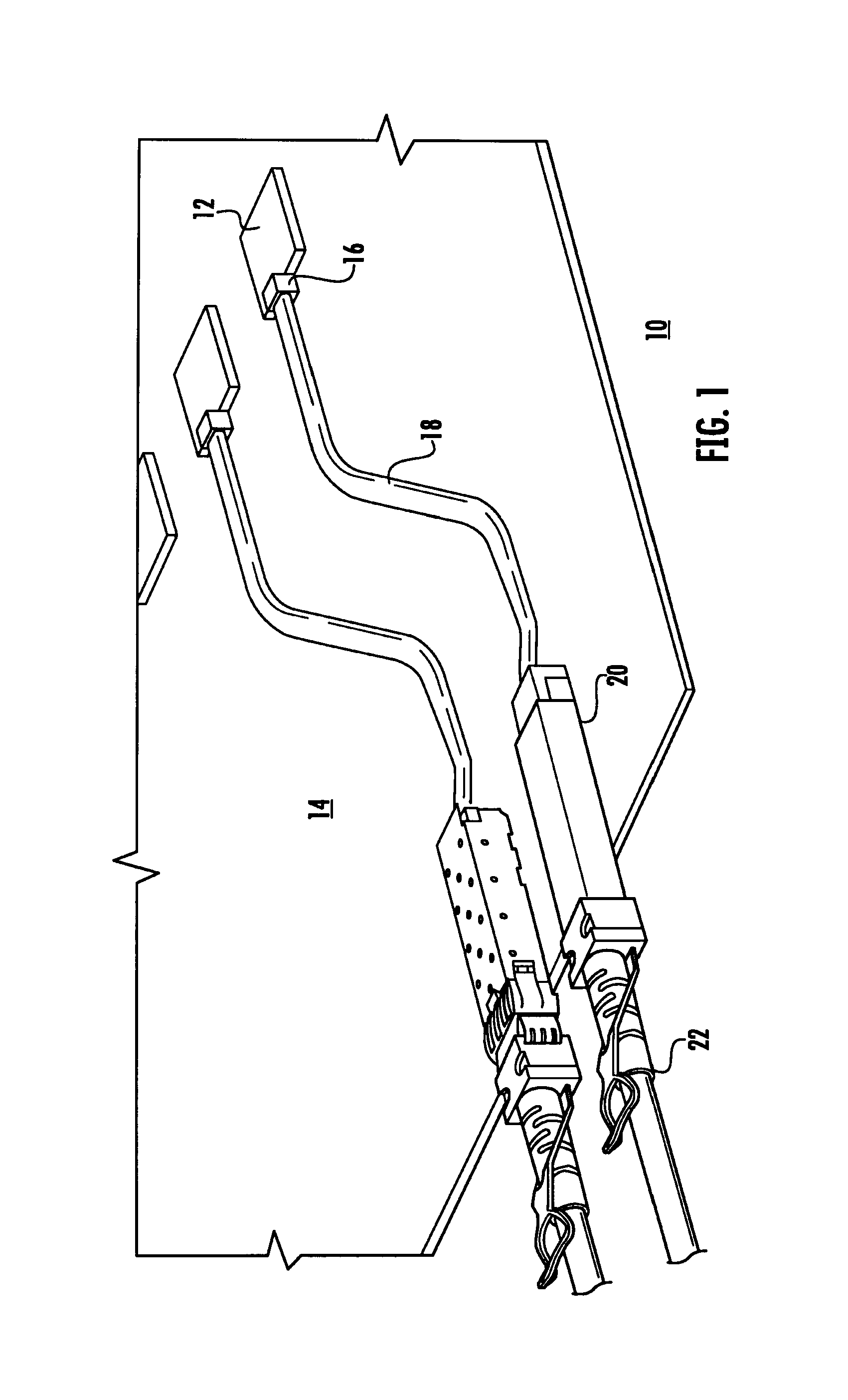
Referring more specifically to FIG. 1, high speed interconnect cable assembly 10 generally comprises chip member 12 mounted on printed circuit board member 14, first connector member 16 interfacing between chip member 12 and bypass cable member 18, and termination member 20 interfacing between bypass cable member 18 and second connector member 22 disposed at the edge of printed circuit board member 14.
Preferably, chip member 12 may comprise a PHY Chip, or any other surface-mounted, physical layer device, known in the art, from which a high speed signal is generated, such as an ASIC and transmitted to a cable assembly. Chip member 12 is mounted to any currently-known printed circuit board, using preferably any of the various currently-known mounting means. Preferably, an FR-4 type printed circuit board is used, in an effort to take advantage of its low cost and wide usage. For purposes of the Present Disclosure, the generated high speed signal may be any type of signal, but typically a data signal, generally having a frequency of 5 GHz and above, and most preferably and is a data signal having a frequency of 10 GHz or more.
Bypass cable member 18 is connected to chip member 12 by means of first connector member 16. First connector member 16 is capable of transmitting a signal greater than 10 GHz between chip member 12 and bypass cable member 18. The interface between first connector member 16 and chip member 18 may be by any known means, including, for example, a plug-receptacle connection, a friction-based connection or the like. It is preferred that the interface be removable. First connector member 16 is preferably capable of receiving the high speed signal generated by the chip member and transmitting it to the bypass cable member without need for a repeater or an amplifier, and without having to use the conductive properties of printed circuit board 14.
Bypass cable member 18 comprises a flexible circuit member, such as a cable, extending from first connector member 16 to termination member 20. Preferably, bypass cable member 18 is capable of receiving and carrying signals above 10 GHz. Preferably, bypass cable member 18 includes one or more wire pairs that transmit differential signals at high speeds. Each such wire pair may have a ground, or drain, wire associated with it. Further, the pairs may be enclosed within bypass cable member 18 and within an associated cable shield. Like first connector member 16, bypass cable member 18 is preferably capable of receiving the high speed signal generated by first connector member 18 and transmitting it to termination member 20 without need for a repeater or an amplifier, and without having to use the conductive properties of printed circuit board 14.
Termination member 20 is electrically connected to bypass cable member 18, and receives the signal from bypass cable member 18. Like all other elements in interconnection assembly 10, termination member 20 is capable of receiving signals greater than 10 GHz. Preferably, termination member 20 is located at or near the edge of printed circuit board 14. Termination member 20 may be mounted to the edge of printed circuit board 14. Alternatively, termination member 20 may be "freestanding," and not connected to any aspect of assembly 10. Termination member 20 may receive bypass cable member 18 though any methods and means as currently described in the art.
Second connector member 22 preferably provides one end of a male-female relationship with termination member 20 (with termination member 20 providing the second end). It is not imperative that second connector member 22 (or termination member 20) be specifically relegated to the male or female end, as the teachings of the Present Disclosure will nevertheless be realized.
Second connector member 22 is preferably not disposed on any other aspect of interconnection assembly 10 of the Present Disclosure, i.e., second connector member 22 is not mounted on printed circuit board 14. Second connector member 22 receives the signal from termination member 20, and transmits the signal to its next or final destination.
The discussion above focused on a single interconnection assembly. Nevertheless, a plurality of interconnection assemblies may be used on a single printed circuit board, each generally comprising the above-referenced elements. A plurality of assemblies is generally illustrated in FIG. 1. Further, in a second embodiment, which is illustrated in FIG. 2, lamination member 24 may encompass all or part of multiple bypass cable members 18 for ease in assembly, as well as to maintain order on printed circuit board 14 and reduce the cost of assembly 10. Preferably, lamination member 24 may comprise a rigid, formable polymer material that can be molded over both first connector member 16 and bypass cable member 18.
Further, in another embodiment, a plurality of interconnection assemblies, used on a single printed circuit board, may be channeled to a single termination member 26 for transmission of signals beyond the printed circuit board. As illustrated in FIG. 3, bypass cable members 18 extend from chip members 12, via first connector member 16, towards first via transfer connectors 28. Each via transfer connector 28 allows the signal being carried in bypass cable members 18 to pass through holes (or vias) in the printed circuit board where they connect with termination member 26.
FIG. 4 illustrates a perspective close up of the connection of via transfer connectors 28 to termination member (not shown in FIG. 4). As illustrated, each via transfer connector 28 houses the termination of bypass cable members 18. Individual wires 30 extending from bypass cable members 18 are mounted within connector housing 32. Connector housing 32, along with individual wires 30 and a portion of bypass cable members 18, are overmolded with terminal housing .[.34.]. .Iadd.38.Iaddend.. Terminal housing .[.34.]. .Iadd.38 .Iaddend.is then inserted into the via hole of the printed circuit board, where it couples to termination member.
FIG. 5 illustrates a perspective close up of first connector member 16. As illustrated, each first connector 16 houses the termination of bypass cable members 18. Individual wires 36 extending from bypass cable members are overmolded with terminal housing 38. Terminal housing 38 is then coupled to chip member 12.
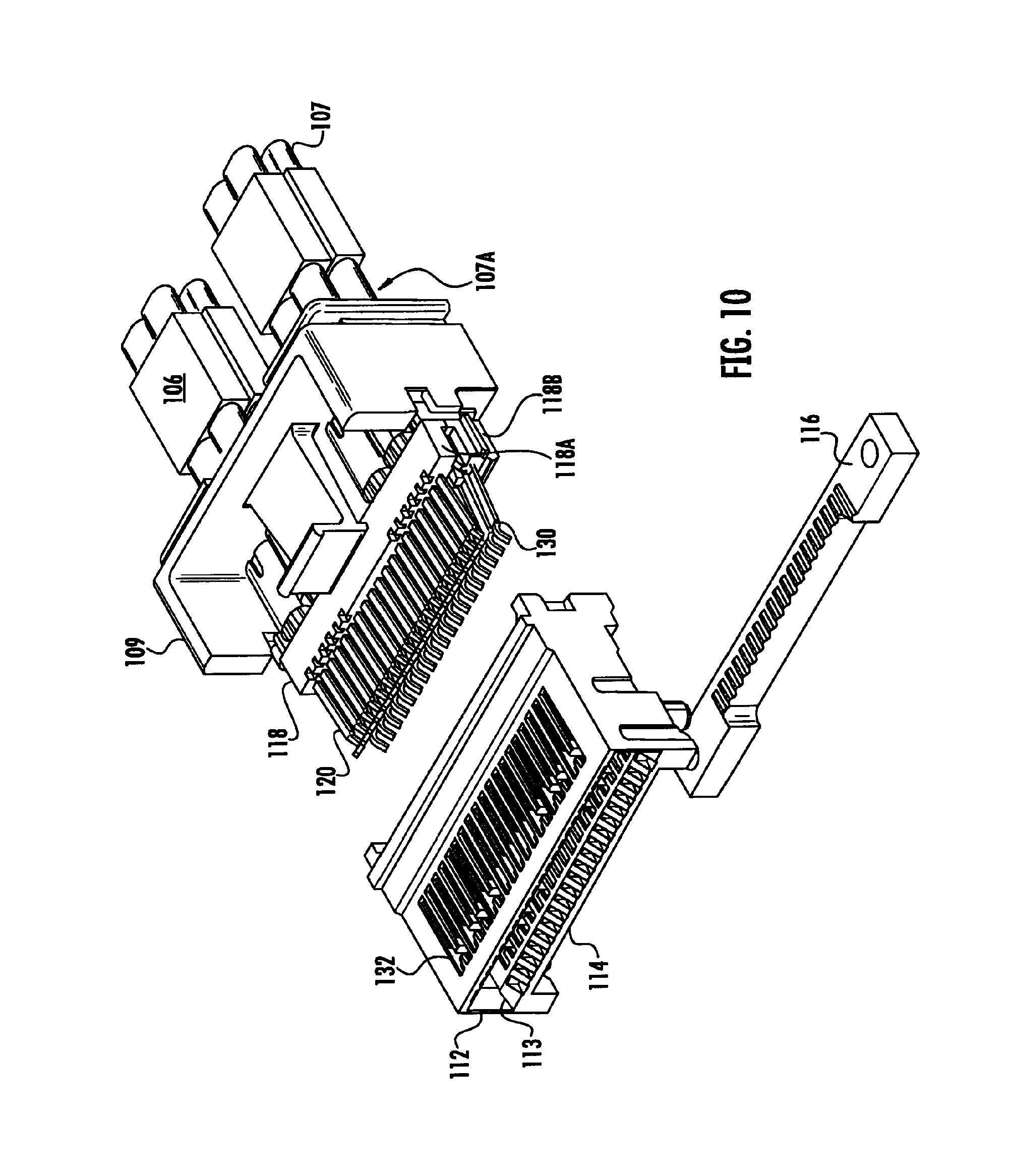
FIGS. 6-13E illustrate another embodiment of a bypass cable assembly 100 constructed in accordance with the principles of the Present Disclosure. As shown in FIG. 6, a circuit board 101 that is used in an electronic device (not shown) has mounted thereon a chip member 104, such as an ASIC, at one location and a shielding cage 102 mounted to the circuit board at another location, remote from the one location. The shielding cage 102 houses a receptacle connector assembly 110 that includes a receptacle connector 112 configured to receive the mating blade (typically the leading edge of a circuit card) of an opposing, mating connector (not shown) in a elongated card-receiving slot 113. The connector 112 may also include a channel 114 disposed underneath the card slot 113 to receive a polarizing member of the mating connector. The connector 112 is accessible through an opening 103 at one end of the shielding cage 102. A portion of the shielding cage 102 extends past the edge of the circuit board 101 and out of the enclosure which houses the circuit board 101. This opening 103 permits access to the connector 112 from the exterior of the device and permits the insertion of a mating connector, typically in the form of a plug connector, therein in order to connect the device to another device and permit the transfer of signals between them.
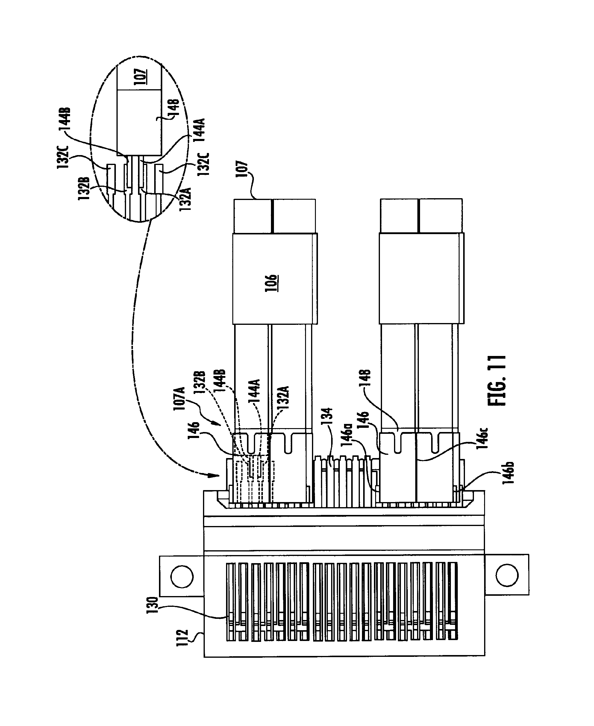
A bypass cable assembly 105 is provided to connect together, the connector 112 and the chip member 104, in order to form a signal transmission line extending therebetween for transmitting signals at high speeds of approximately 5 GHz and greater and preferably of approximately 10 GHz and greater. The cable assembly 105 includes a preselected length of cable 107 that has at a first end 107a thereof, a first termination assembly and at a second and opposite end 107b thereof, a second termination assembly. As shown best in FIG. 12B, each cable 107 may be of the "twin-ax" type, in which a pair of signal conductors 144A, 144B are positioned in spaced-apart relationship within an insulative body 142. This cable body 142 is surrounded by an outer conductive shielding layer 148 that is located underneath an exterior, insulative covering 140 and all of the cable elements may be formed as the single component illustrated. The structure of this particular type of twin-ax cable lends itself to uniformity throughout its length so that a consistent impedance profile is attained for the length of the cable. The cable assemblies 105 of this disclosure may include as few as one or two cables, or they may include greater numbers, such as the eight cables shown in FIGS. 6, 9 & 11.
In order to avoid losses that normally occur in the use of signal transmission lines in the circuit board 101 using FR-4 as the board material, the cables 107 are used as the signal transmission lines. As noted above, the cables 107 are made in a manner that controls their size, thickness and the position and spacing of the signal conductors 144A, 144B so as to define a constant impedance profile throughout the lengths of the cables. Accordingly, twin-ax type of cable is desirable as well as flexible circuitry where positioning of the conductors and insulators may be controlled to a high degree of tolerance. Problems with impedance profiles typically occur at the termination points of cables where the geometry of the cable disrupted in order to effect a termination. One such solution to this problem is disclosed in U.S. Pat. No. 6,454,605, issued Sep. 24, 2002 and assigned to the assignee of the Present Disclosure and which is hereby incorporated by reference, in its entirety.
The cable assemblies of the Present Disclosure are terminated at their opposite ends 107A, 107B in a manner that seeks to reduce the modification of the cable geometry in order to reduce the magnitude of the aforementioned discontinuities and to prevent to the extent possible excessive loss, noise and crosstalk. Returning to the drawings and in particular FIGS. 12 & 12A, it can be seen that the terminals 120 of the receptacle connector 112 have tail portions 132 that extend outwardly from the rear face of the terminal assembly supports 118A, 118B and contact portions 130 that extend forwardly within the card-receiving slot 113 of the body of the receptacle connector 112. The terminal contact and tail portions 130, 132a, 132b, extend in a continuous, generally horizontal extent through the connector without any vertical terminal extents that would provide an interruption of the horizontal extent. Consequently, as used herein, the term uninterrupted means a generally horizontal extent without any vertical portions. Similarly, "generally horizontal extent" also means that there are no vertical portions of the terminals that change the levels of the terminal contact and tail portions as would be found in terminals configured for surface mounting such as the low speed, power and status terminals 134 that are interposed between the high speed terminal sets. These non-high speed terminals 134 may be positioned with the use of a tail aligner block 116 or the like. In order to provide strain relief and to facilitate assembly, two cables may be held together by a block 106 applied to the cables 107 downstream of the termination areas.
In this manner, a "direct connection" is effected between the cable first end 107A and the connector 112, in a manner such that the signal terminal tail portions 132a, 132b are aligned with the exposed leads of the cable conductors 144A, 144B so that the exposed leads may be placed on the flat surfaces which the terminal tail portions 132a, 132b preferably provide. The inner shielding 148 of each cable 107 is pulled back over the exposed end of the cable and a shield extension 146 is provided for engaging these cable ends. The extension 146 is shown as a dual extension that can accommodate two cables. The shield extension 146 has what may be considered a cup portion 145 that is formed in a configuration that is generally complementary to the exterior configuration of the cable 107, and it is provided with contact feet 146a-c for contacting the associated terminal tail portions 132c of ground terminals in the receptacle connector 112.
The dual shield extension 146 shown in the drawings has two such cup portions 145 and three contact feet. Two contact feet 146a, 146b are formed along the outer edges of the cup portion 145, while the third contact foot 14c is formed between the cup portions 145. The contact surfaces 147 formed on the bottom of the contact feet are preferably aligned with each other along a common plane, shown as "H" in FIG. 12B. The conductors 144A, 144B of the cable 107 are also preferably aligned with the contact feet, along H as illustrated best in FIG. 12B. In this manner a "direct" connection is effected between first ends 107A of the cables 107 and the board mounted connector 112, thereby eliminating the need for surface mounting or through hole mounting of the connector high speed terminal tails, all of which contribute to loss, noise and crosstalk at high speeds. Terminals of the connector 112 for which high speed performance is not an issue, such as low speed signal terminals and/or power and status terminals 134, may be terminated in conventional manners mentioned above and they are shown in FIGS. 12 & 12A as surface mounted, and such terminals may be disposed between sets of high speed terminals as illustrated for additional separation between the high speed terminal sets. Removing the high speed signals of the receptacle connector from attachment directly to the board, reduces the cost in formation and manufacture of the circuit board 102. Additionally, the termination style shown in the drawings mirrors the geometry of the cable and provides generally complete shielding at the direct connection.
The shield extensions 146 provide as close as can be attained complete shielding at the direct termination to the board connector and they extend forwardly to completely cover the exposed ends of the cable signal conductors 144A, 144B as shown in FIG. 11. The shield extension mounting feet 146a-c thereof are spaced apart and contact opposing tail portions of ground terminals of the first connector 112. The shield extension feet 146a-c and the conductors 144A, 144B of the cables 107 can be soldered or welded in their attachment to the connector terminals and the shield extensions 146 may be attached to the cables 107 by contact, a conductive adhesive, soldering or other suitable means. In this manner, the cable geometry is closely replicated in the termination area and more effective shielding is provided than just an ordinary ground wire to ground terminal connection. An EMI housing 109 may be utilized to provide an enclosure, in combination with the shielding cage 102 about the cable termination area.
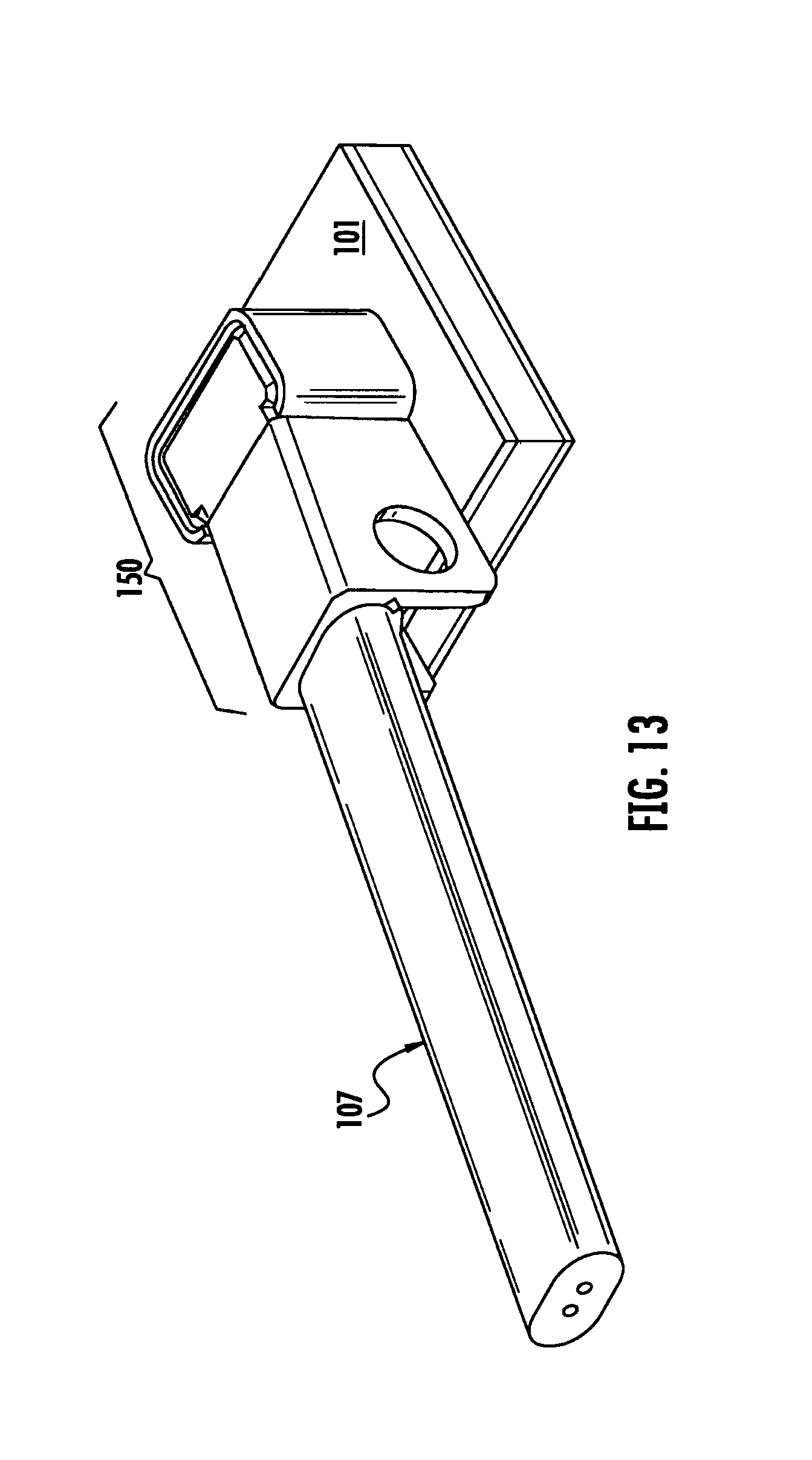
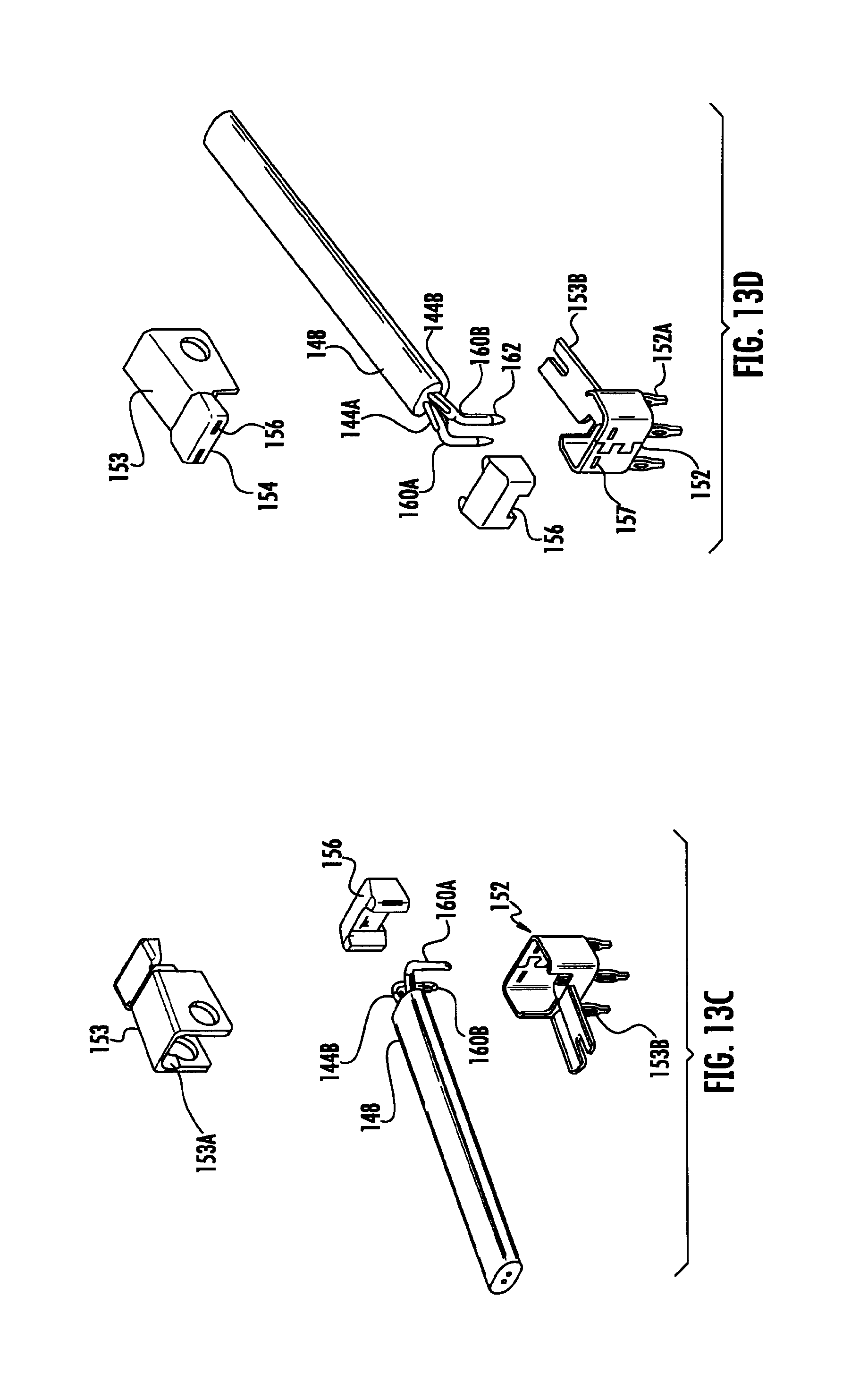
FIGS. 13A-D illustrate one form of termination that may be applied to the second ends of the cables 107, which may be either connected directly to the chip member or to the circuit board 101 in close proximity thereto. As illustrated in FIGS. 13B-D, the exposed leads of the cable conductors 144A, 144B are attached to signal terminals 160, shown as a pair of signal terminals 160A, 160B. These terminal preferably have flat tail portions 163 and through hole contact portions 162. The flat tail portions 163 preferably provide a flat surface to which the exposed conductors 144A, 144B may be contacted and attached via solder, welding or the like. The signal terminal 160 may be held in by an insulative support 156 that as shown is molded over body portions of the terminal 160, leaving the tail and contact portions 163, 162 exposed for termination purposes. A shield collar 152 is provided that houses the signal terminal support 156 and substantially encloses the signal terminals with a conductive shield. The shield collar 152 has a shield extension 153B that is similar in configuration to cable first end shield extensions 146 in that is has a cup portion 145 that contacts and receives the cable 107 and its inner shielding 148 therein. A cap member 153 is also provided and the cap member includes a block portion 154 that preferably abuts the terminal support 156 and which further preferably engages the shield collar 152 by way of tabs 156 that engage like holes 157 in the walls of the collar 152.
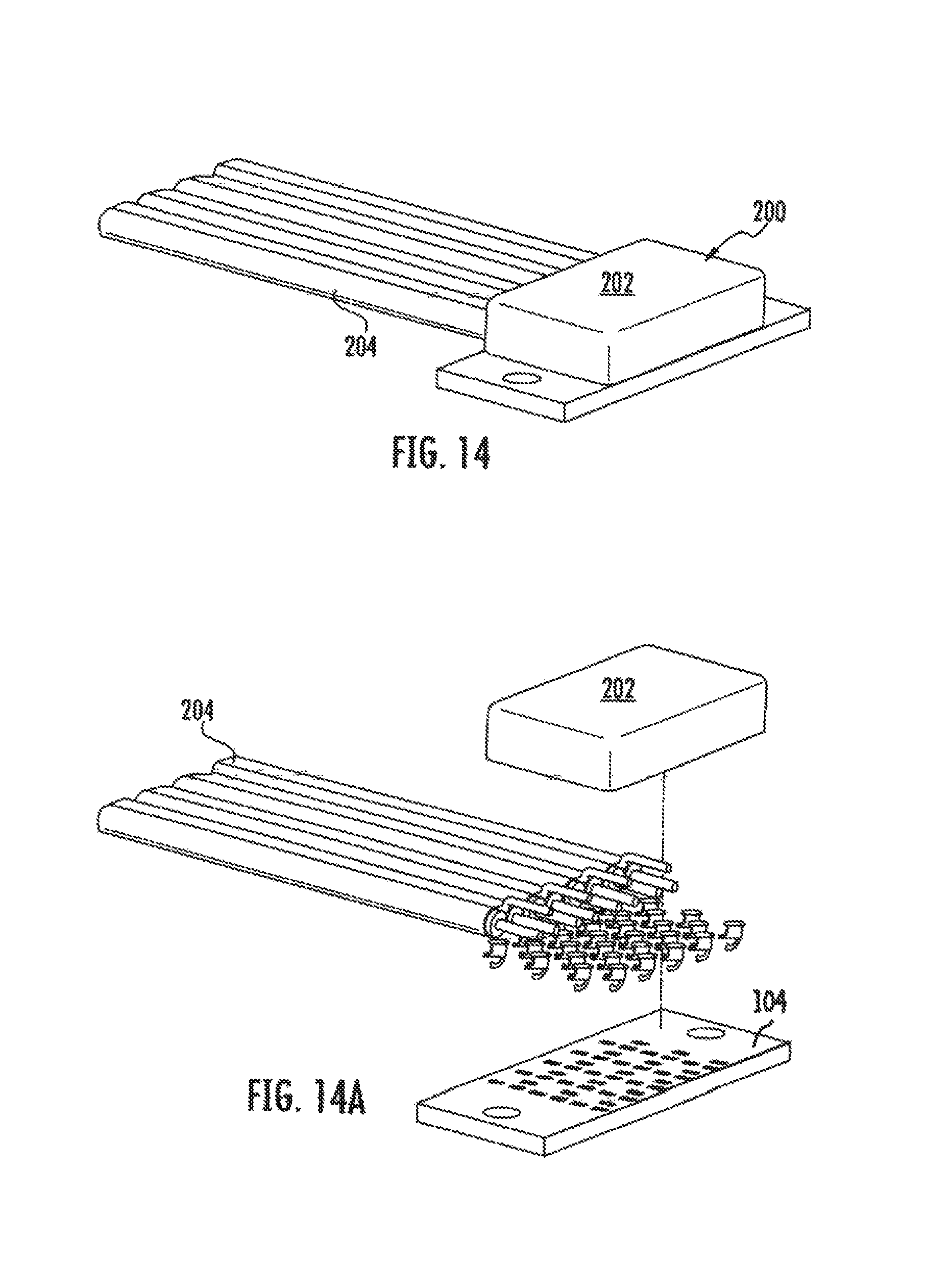
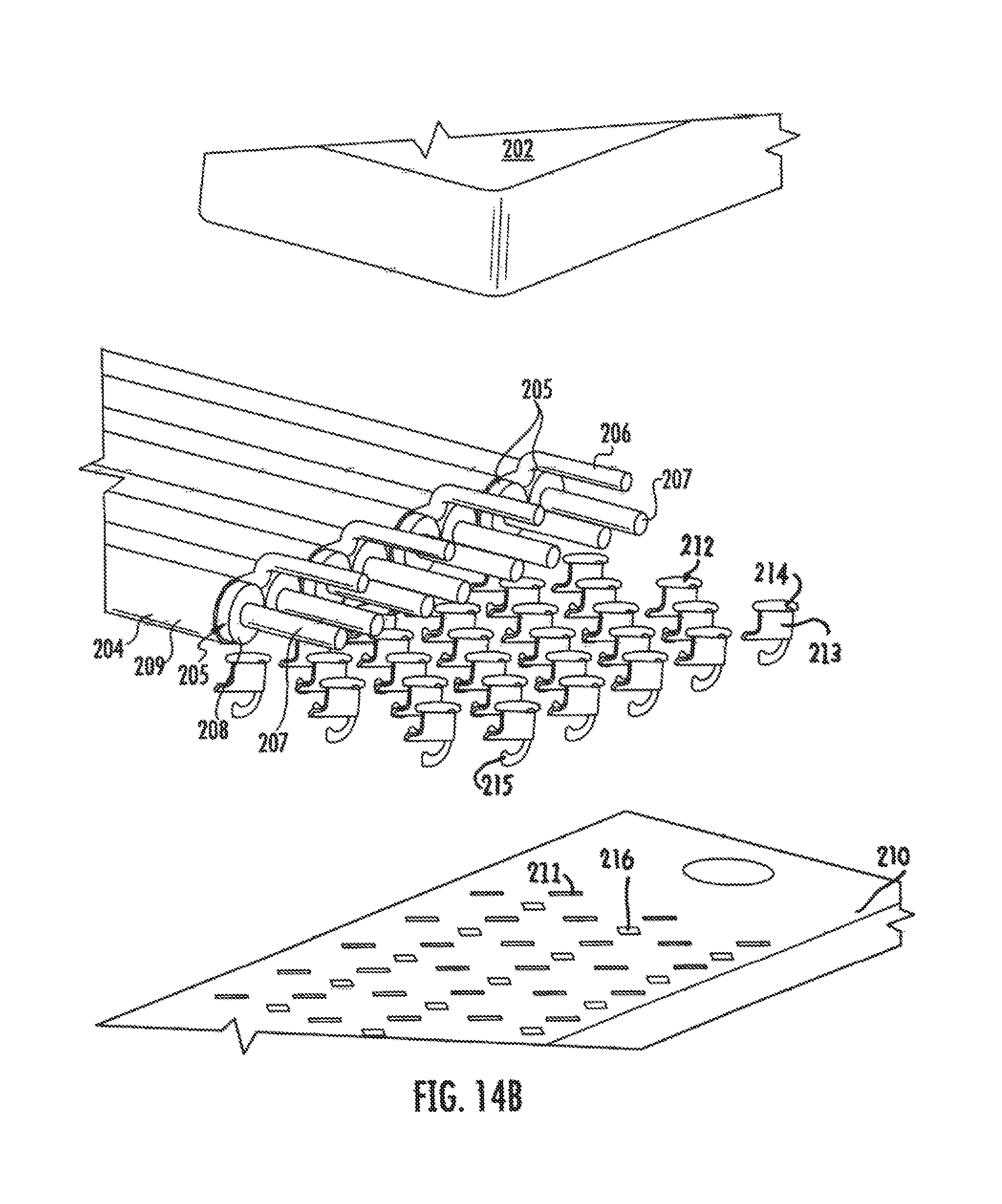
FIGS. 14-14B illustrate another embodiment of a manner or termination to a second connector. In this embodiment, the second connector 200 is one that is used to attach directly to the chip member 104, and typically to a top surface thereof. In this regard, the second connector 200 has a housing 202 that receives a plurality of cables 204, and the type of cables illustrated are of a different twin-ax structure, namely one in which each cable 204 contain a pair of signal wires 205 and a drain (ground) wire 206. The signal wires 205 have signal conductors 207 running their length and surrounded by an outer insulative covering 208 and an outer covering 209 is provided that encloses a pair of the signal wires 205 and an associated drain wire 206. A perforated base portion 210 of the housing 202 has a plurality of slots, or cavities 211, each of which is configured to receive a single terminal 212 therein. LGA-style terminals are illustrated and each such terminal 212 includes a body portion 213 that engages the housing cavity 211, a tail portion or mounting stub 214 that extends out of the cavity 211 and into contact with an exposed conductor 207 of the signal wires 205, and a contact portion 215 that extend out of the opposite end of the cavity 211. The second connector 200 also includes second cavities 216 that receive ground terminals (not shown) that are connected at their upper ends to the drain wires 206 and at their lower ends to the chip member 104. The termination arrangement of this connector 200 also maintains, to the extent possible the geometry of the cables 204 through the connector termination, in the sense that the triangular arrangement of the three wires of each cable is maintained until the point where the drain wire is attached to the ground terminal and then the extent of the ground terminal is spaced from the ends of the signal wire terminals 212 as evidenced by the pattern of the first and second terminal cavities 211, 216.
FIG. 15 illustrates an alternate construction for use as a signal transmission line in accordance with the disclosure and takes the form of an extent of flat flexible circuitry 300. The extent includes a pair of signal conductors 302 that are spaced apart from each other and which run lengthwise between opposite ends of the cable 300. The conductors 302 are surrounded on their top and bottom surfaces and sides by insulative portions 304, 305. Ground shields 306 are provided to enclose the signal conductors 302, and although shown only as above and below the signal conductors 302, it will be understood that they may be disposed alongside of the signal conductors. With this sort of structure, the signal conductors may be exposed and aligned with terminal tails, while the ground shield extended to cover the termination areas in a manner similar to that shown above.
FIG. 16 is a graph comparing the loss between two 12-inch lengths of signal transmission lines, with one of the transmission lines comprising a pair of circuit traces formed in or on FR-4 circuit board material and the other transmission line comprising cables of the Present Disclosure. It can be seen from FIG. 16 that the use of the cable of the Present Disclosure leads to a very low loss transition that only breaks past the 5 dB mark at approximately the 20 GHz frequency. Within the range of testing error, we believe that the cables of the Present Disclosure have low loss characteristics of no greater than between about 5 dB and about 8 dB at frequencies greater than about 19 Ghz.
While a preferred embodiment of the Present Disclosure is shown and described, it is envisioned that those skilled in the art may devise various modifications without departing from the spirit and scope of the foregoing Description and the appended Claims.
* * * * *
References
D00000
D00001
D00002
D00003
D00004
D00005
D00006
D00007
D00008
D00009
D00010
D00011
D00012

D00013

D00014

D00015
D00016

D00017

D00018
D00019

D00020
D00021
D00022

D00023

XML
uspto.report is an independent third-party trademark research tool that is not affiliated, endorsed, or sponsored by the United States Patent and Trademark Office (USPTO) or any other governmental organization. The information provided by uspto.report is based on publicly available data at the time of writing and is intended for informational purposes only.
While we strive to provide accurate and up-to-date information, we do not guarantee the accuracy, completeness, reliability, or suitability of the information displayed on this site. The use of this site is at your own risk. Any reliance you place on such information is therefore strictly at your own risk.
All official trademark data, including owner information, should be verified by visiting the official USPTO website at www.uspto.gov. This site is not intended to replace professional legal advice and should not be used as a substitute for consulting with a legal professional who is knowledgeable about trademark law.