Electronic device housing
Alfredsson , et al. June 1, 2
U.S. patent number D920,939 [Application Number D/687,685] was granted by the patent office on 2021-06-01 for electronic device housing. This patent grant is currently assigned to ABB Power Grids Switzerland AG. The grantee listed for this patent is ABB Power Grids Switzerland AG. Invention is credited to Fredrik Alfredsson, Mikael Edoff.


| United States Patent | D920,939 |
| Alfredsson , et al. | June 1, 2021 |
Electronic device housing
Claims
CLAIM The ornamental design for an electronic device housing, as shown and described.
| Inventors: | Alfredsson; Fredrik (Vasteras, SE), Edoff; Mikael (Saltsjo-Boo, SE) | ||||||||||
|---|---|---|---|---|---|---|---|---|---|---|---|
| Applicant: |
|
||||||||||
| Assignee: | ABB Power Grids Switzerland AG
(Baden, CH) |
||||||||||
| Appl. No.: | D/687,685 | ||||||||||
| Filed: | April 15, 2019 |
Foreign Application Priority Data
| Oct 15, 2018 [EM] | 005798378 | |||
| Apr 5, 2019 [EM] | 006370771 | |||
| Current U.S. Class: | D13/184; D13/110; D13/123 |
| Current International Class: | 1303 |
| Field of Search: | ;D13/110,123,158,162,184,199 ;D14/301,439 |
References Cited [Referenced By]
U.S. Patent Documents
| D348269 | June 1994 | Chong |
| D373362 | September 1996 | Kuroiwa |
| D424529 | May 2000 | Raspotnig |
| D437586 | February 2001 | Sonntag |
| D493771 | August 2004 | Pagella |
| D506977 | July 2005 | Lee |
| D643376 | August 2011 | Naumann |
| D702198 | April 2014 | Gretz |
| D707187 | June 2014 | Mauchle |
| D719105 | December 2014 | Shin |
| D762495 | August 2016 | Tanaka |
| D772171 | November 2016 | Ohmori |
| D823798 | July 2018 | Gleave |
| D860957 | September 2019 | Gao |
| D867304 | November 2019 | Tsurumi |
| 10547161 | January 2020 | Lin |
| D877701 | March 2020 | Byrne |
| 10707768 | July 2020 | Voegeli |
| 2004/0008492 | January 2004 | Kato |
| 2011/0222244 | September 2011 | Takashiro |
| 2011/0242770 | October 2011 | Yamanaka |
| 2013/0016481 | January 2013 | Takahashi |
| 2019/0165687 | May 2019 | Yamazawa |
| 2020/0059163 | February 2020 | Koshii |
Other References
|
ABB Launches new microgrid system to boost use of renewables; Oct. 10, 2016; 1 pg.; https://www.windpowerengineering.com/abb-launches-new-microgrid-system-bo- ost-use-renewables/. cited by examiner . Rolls-Royce and ABB partner to develop micorgrid solution for business; Apr. 2, 2019; 1 pg. ; https://www.edie.net/news/8/Rolls-Royce-and-ABB-partner-to-develop-microg- rid-solution-for-business/. cited by examiner. |
Primary Examiner: Sikder; Selina
Attorney, Agent or Firm: Slater Matsil, LLP
Description
FIG. 1 is a top, front isometric view of an electronic device housing in accordance with the new design;
FIG. 2 is a right side elevational view of FIG. 1;
FIG. 3 is a left side elevational view of FIG. 1;
FIG. 4 is a front elevational view of FIG. 1;
FIG. 5 is a rear elevational view of FIG. 1;
FIG. 6 is a top plan view of FIG. 1; and,
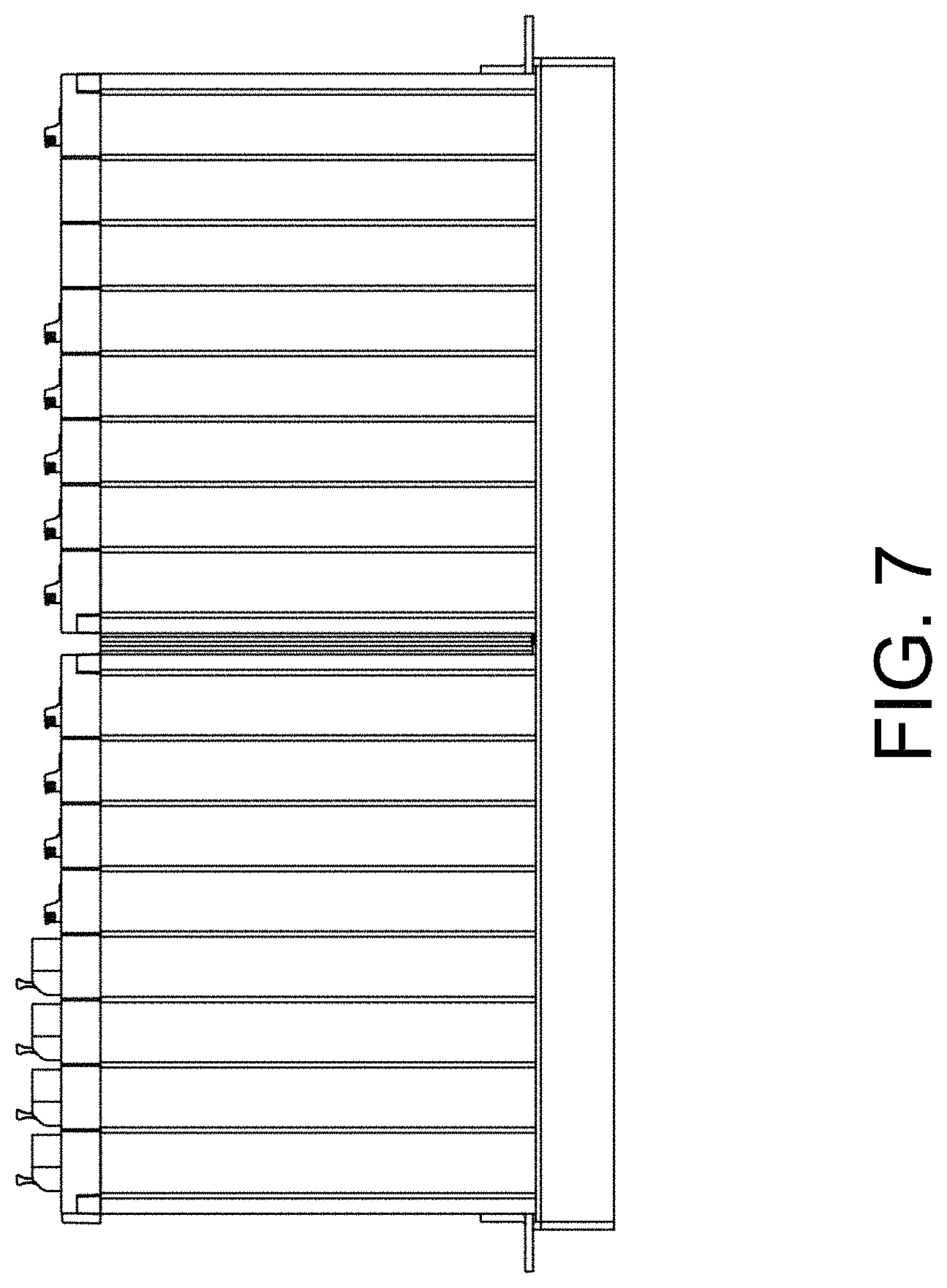
FIG. 7 is a bottom plan view of FIG. 1.
* * * * *
References
D00000
D00001
D00002
D00003
D00004
D00005
D00006
D00007
XML
uspto.report is an independent third-party trademark research tool that is not affiliated, endorsed, or sponsored by the United States Patent and Trademark Office (USPTO) or any other governmental organization. The information provided by uspto.report is based on publicly available data at the time of writing and is intended for informational purposes only.
While we strive to provide accurate and up-to-date information, we do not guarantee the accuracy, completeness, reliability, or suitability of the information displayed on this site. The use of this site is at your own risk. Any reliance you place on such information is therefore strictly at your own risk.
All official trademark data, including owner information, should be verified by visiting the official USPTO website at www.uspto.gov. This site is not intended to replace professional legal advice and should not be used as a substitute for consulting with a legal professional who is knowledgeable about trademark law.