Electroencephalogram signal amplification device
Levine , et al. May 18, 2
U.S. patent number D919,818 [Application Number D/679,098] was granted by the patent office on 2021-05-18 for electroencephalogram signal amplification device. This patent grant is currently assigned to X Development LLC. The grantee listed for this patent is X Development LLC. Invention is credited to Haden Cory, Matthew David Day, Gabriella Levine.
| United States Patent | D919,818 |
| Levine , et al. | May 18, 2021 |
Electroencephalogram signal amplification device
Claims
CLAIM The ornamental design for an electroencephalogram signal amplification device, substantially as shown and described.
| Inventors: | Levine; Gabriella (San Francisco, CA), Cory; Haden (San Francisco, CA), Day; Matthew David (Oakland, CA) | ||||||||||
|---|---|---|---|---|---|---|---|---|---|---|---|
| Applicant: |
|
||||||||||
| Assignee: | X Development LLC (Mountain
View, CA) |
||||||||||
| Appl. No.: | D/679,098 | ||||||||||
| Filed: | February 1, 2019 |
| Current U.S. Class: | D24/186 |
| Current International Class: | 2402 |
| Field of Search: | ;D10/104.1,101,75 ;D14/188,299,358 ;D13/162 ;D24/186-187 |
References Cited [Referenced By]
U.S. Patent Documents
| D782354 | March 2017 | Lovin |
| D805938 | December 2017 | Park |
| D809951 | February 2018 | Yang |
Attorney, Agent or Firm: Fish & Richardson P.C.
Description
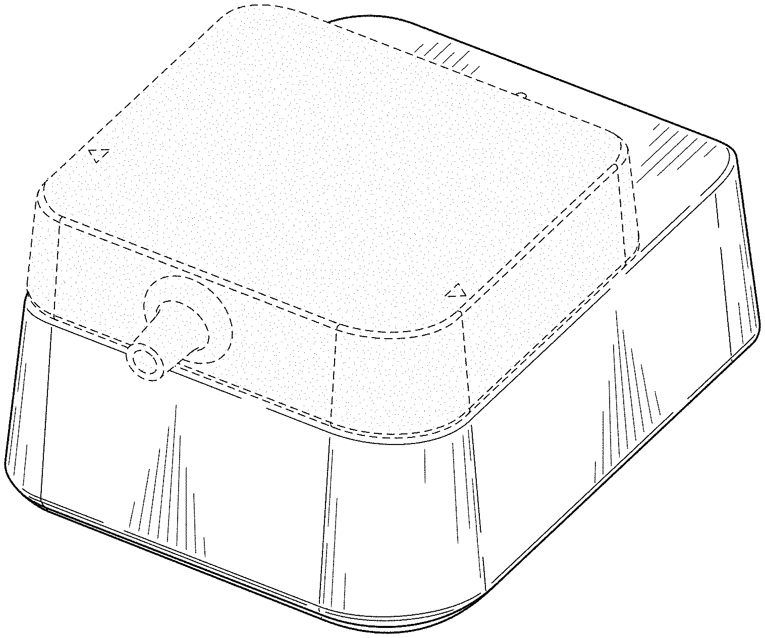
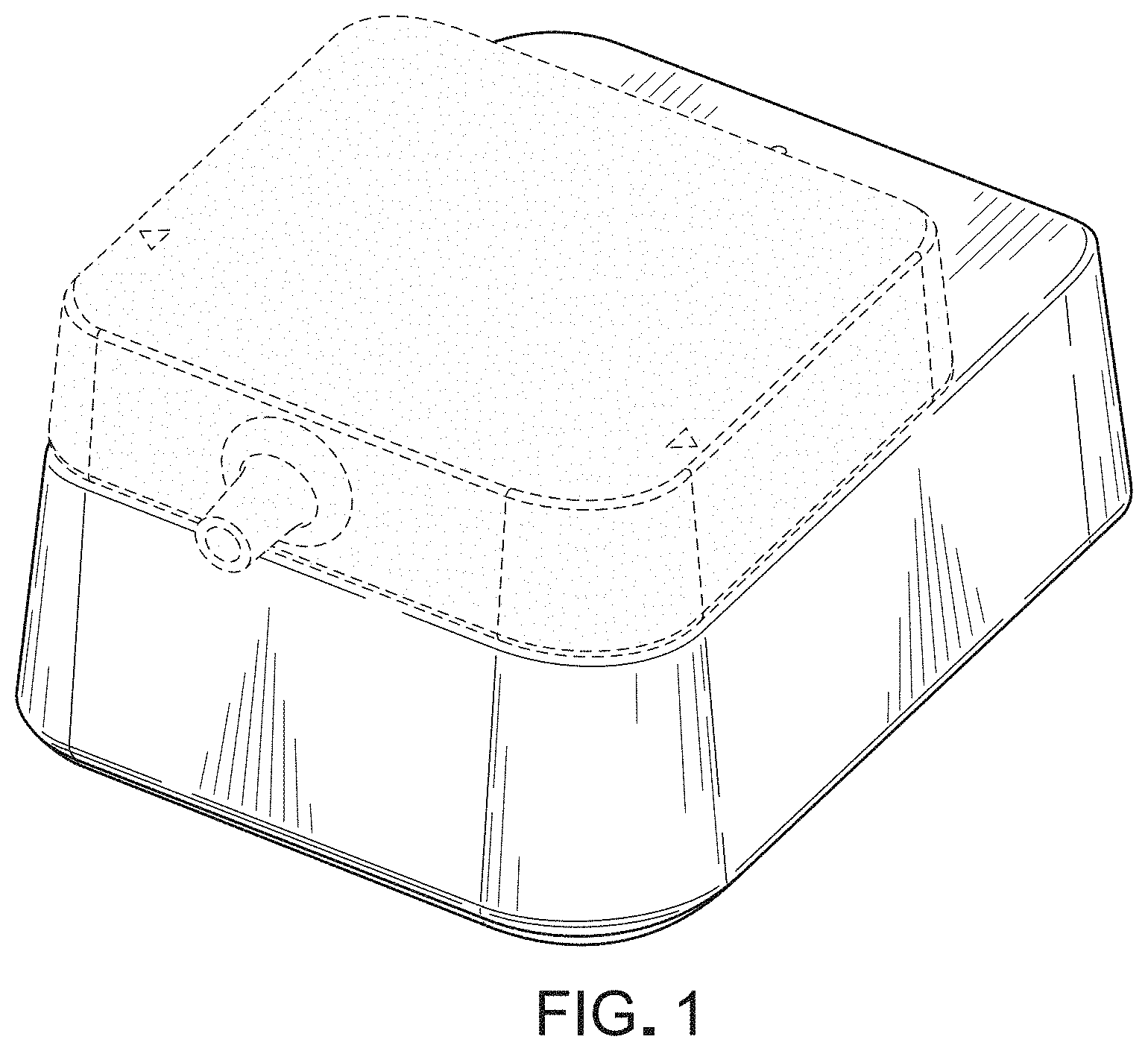
FIG. 1 is a perspective view of an electroencephalogram signal amplification device with an adaptor unit attached to a top surface of the electronic device.
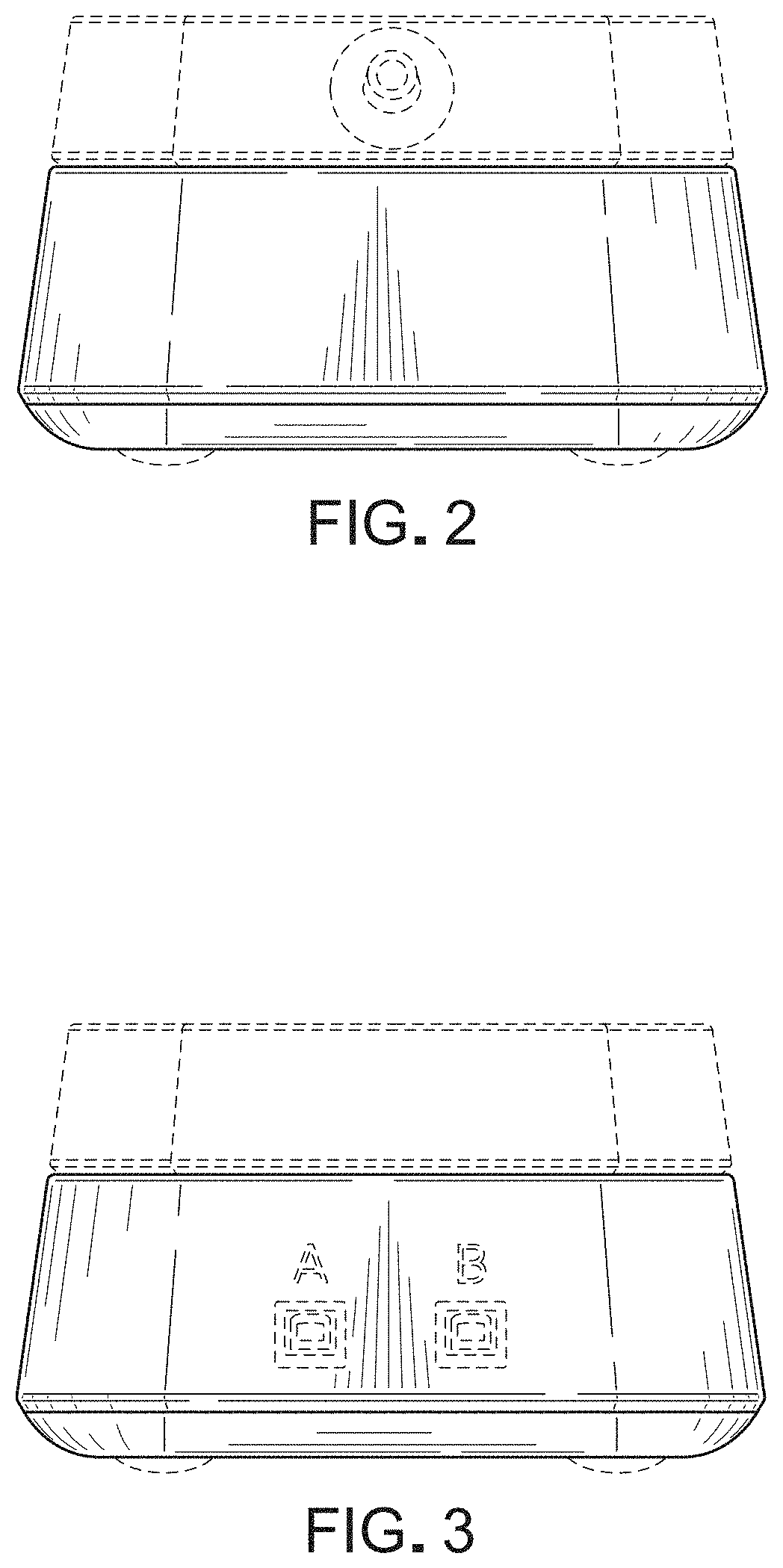
FIG. 2 is a front view of the electronic device of FIG. 1.
FIG. 3 is a rear view of the electronic device of FIG. 1.
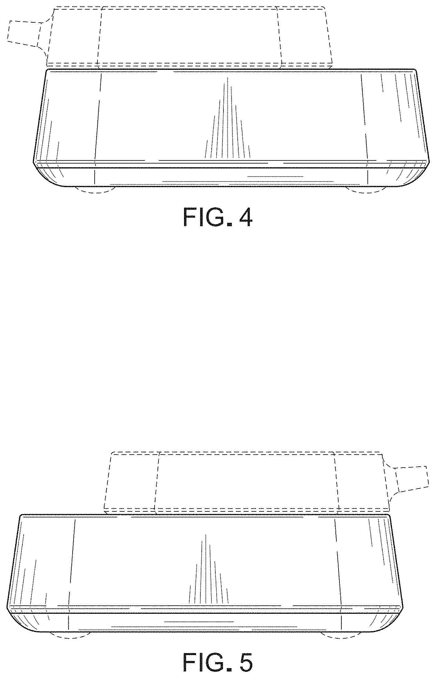
FIG. 4 is a left side view of the electronic device of FIG. 1.
FIG. 5 is a right side view of the electronic device of FIG. 1.
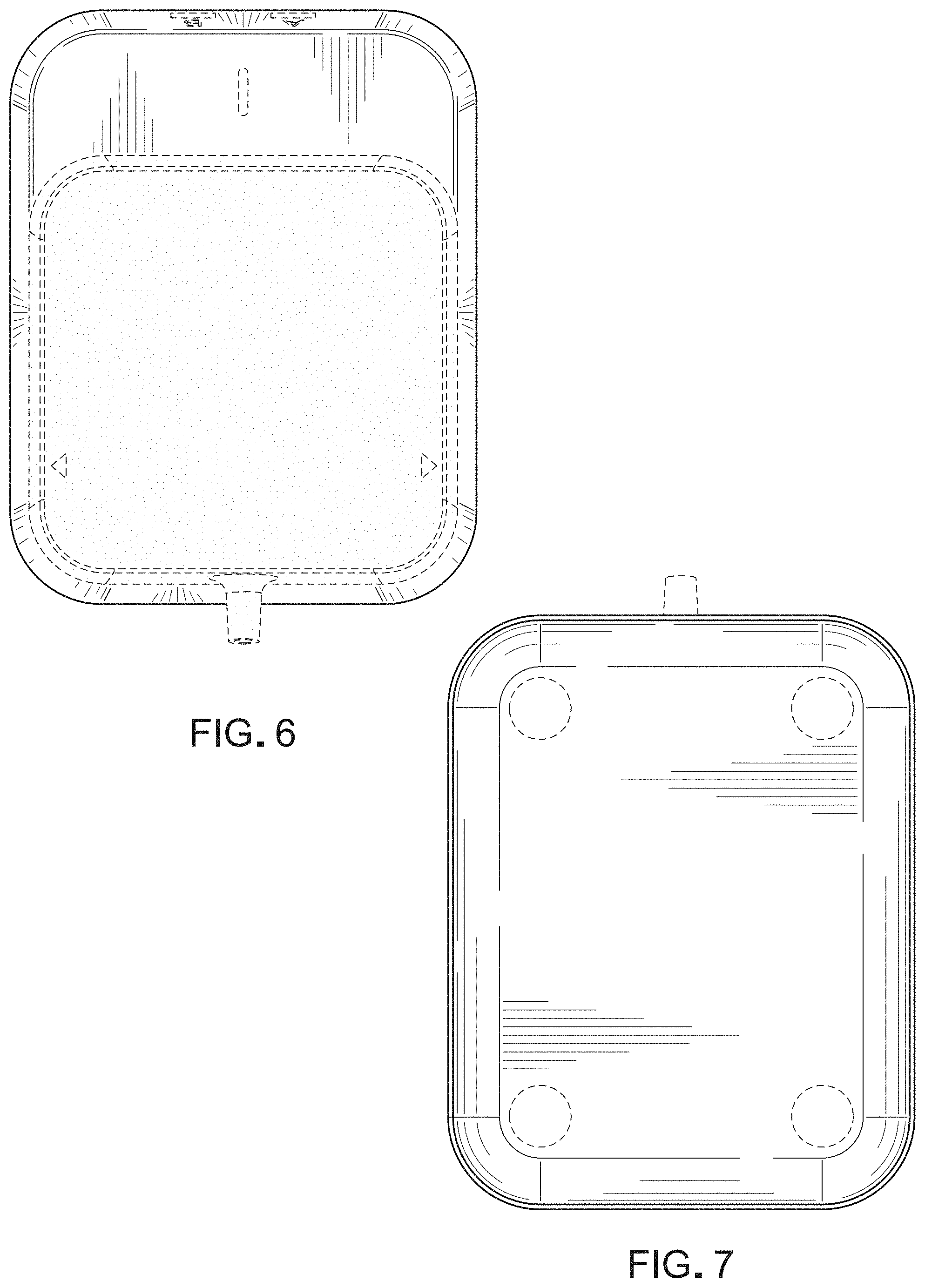
FIG. 6 is a top view of the electronic device of FIG. 1.
FIG. 7 is a bottom view of the electronic device of FIG. 1.
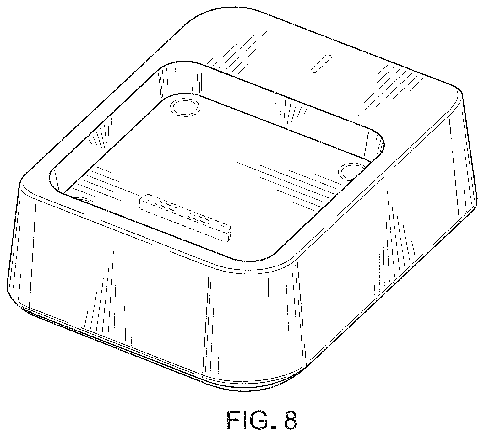
FIG. 8 is a perspective view of the electronic device without the adaptor unit (shown in FIGS. 1-7) attached.
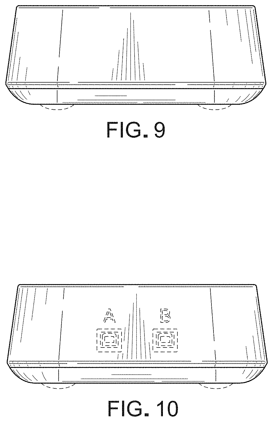
FIG. 9 is a front view of the electronic device of FIG. 8 without the adaptor unit.
FIG. 10 is a rear view of the electronic device of FIG. 8 without the adaptor unit.
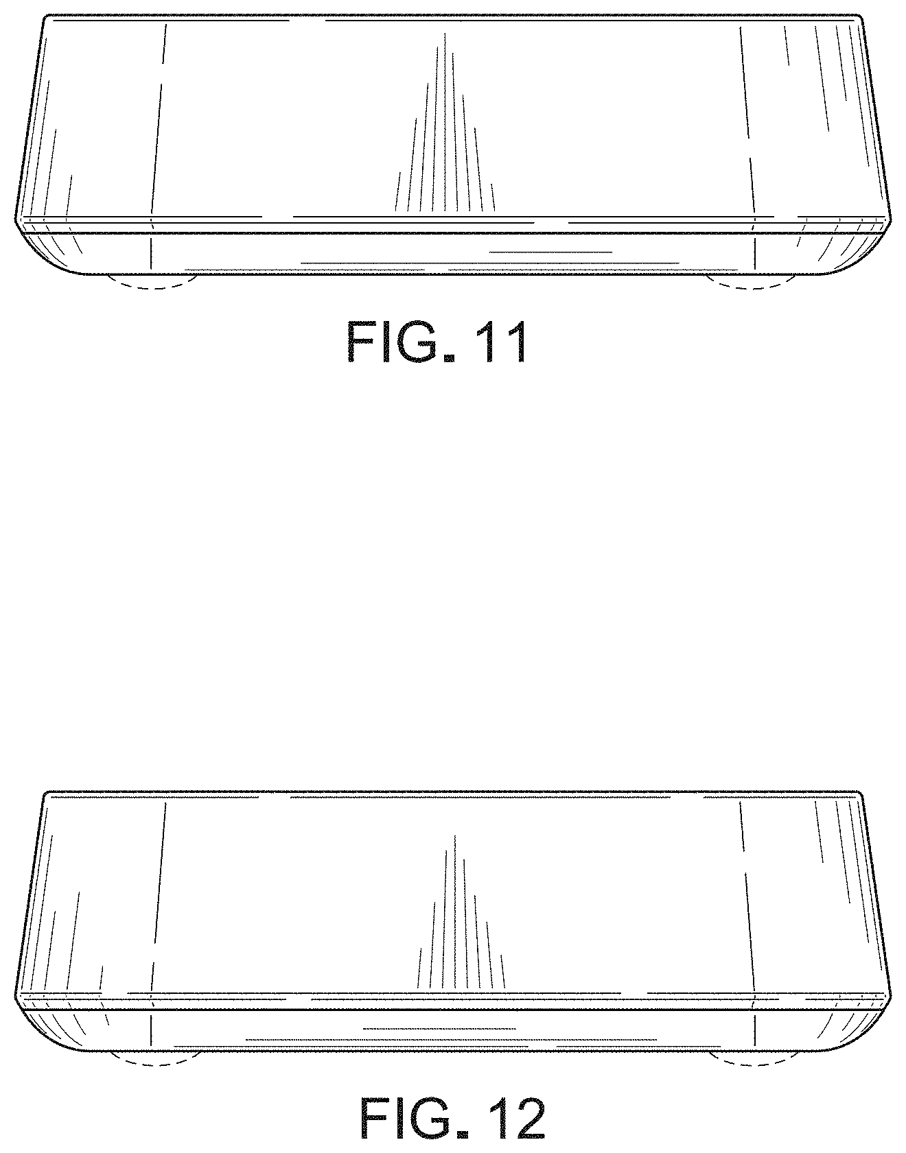
FIG. 11 is a left side view of the electronic device of FIG. 8 without the adaptor unit.
FIG. 12 is a right side view of the electronic device embodiment of FIG. 8 without the adaptor unit.
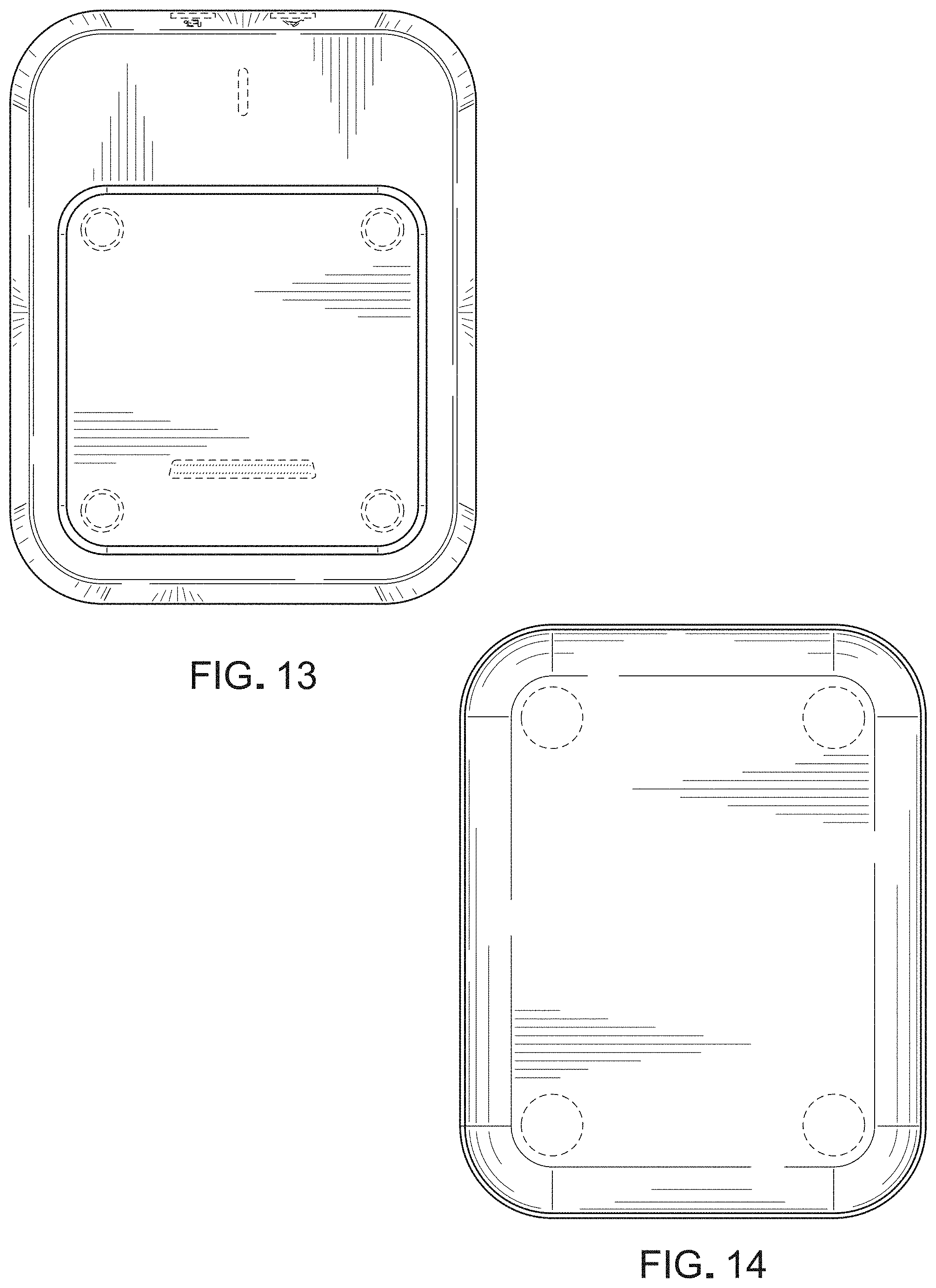
FIG. 13 is a top view of the electronic device of FIG. 8 without the adaptor unit; and,
FIG. 14 is a bottom view of the electronic device of FIG. 8 without the adaptor unit.
The broken lines in each figure illustrate features that form no part of the claimed design. The adaptor unit shown in (FIGS. 1-7) is represented in broken lines and forms no part of the claimed design.
* * * * *
D00000
D00001
D00002
D00003
D00004
D00005
D00006
D00007
D00008
XML
uspto.report is an independent third-party trademark research tool that is not affiliated, endorsed, or sponsored by the United States Patent and Trademark Office (USPTO) or any other governmental organization. The information provided by uspto.report is based on publicly available data at the time of writing and is intended for informational purposes only.
While we strive to provide accurate and up-to-date information, we do not guarantee the accuracy, completeness, reliability, or suitability of the information displayed on this site. The use of this site is at your own risk. Any reliance you place on such information is therefore strictly at your own risk.
All official trademark data, including owner information, should be verified by visiting the official USPTO website at www.uspto.gov. This site is not intended to replace professional legal advice and should not be used as a substitute for consulting with a legal professional who is knowledgeable about trademark law.