Connector terminal
Obata , et al. March 2, 2
U.S. patent number D911,962 [Application Number D/674,911] was granted by the patent office on 2021-03-02 for connector terminal. This patent grant is currently assigned to JAPAN AVIATION ELECTRONICS INDUSTRY, LIMITED. The grantee listed for this patent is Japan Aviation Electronics Industry, Limited. Invention is credited to Yusuke Obata, Hiroaki Obikane.


View All Diagrams
| United States Patent | D911,962 |
| Obata , et al. | March 2, 2021 |
Connector terminal
Claims
CLAIM The ornamental design for a connector terminal, as shown and described.
| Inventors: | Obata; Yusuke (Tokyo, JP), Obikane; Hiroaki (Tokyo, JP) | ||||||||||
|---|---|---|---|---|---|---|---|---|---|---|---|
| Applicant: |
|
||||||||||
| Assignee: | JAPAN AVIATION ELECTRONICS
INDUSTRY, LIMITED (Tokyo, JP) |
||||||||||
| Appl. No.: | D/674,911 | ||||||||||
| Filed: | December 27, 2018 |
Foreign Application Priority Data
| Jul 2, 2018 [JP] | 2018-014553 | |||
| Jul 2, 2018 [JP] | 2018-014554 | |||
| Jul 2, 2018 [JP] | 2018-014555 | |||
| Current U.S. Class: | D13/133 |
| Current International Class: | 1303 |
| Field of Search: | ;D13/110,123,133,146,147,154,118,119,120,149,178,199 |
References Cited [Referenced By]
U.S. Patent Documents
| 5888107 | March 1999 | Seymour |
| 6290556 | September 2001 | Howland |
| D568245 | May 2008 | Kudo |
| 9799976 | October 2017 | Lehner |
| D840942 | February 2019 | DeVito |
| D842811 | March 2019 | Iwasawa |
| D876360 | February 2020 | Obata |
| D882525 | April 2020 | Bhagynathan Sathianathan |
| 2008/0070452 | March 2008 | Komiyama |
| 2012/0003881 | January 2012 | Hora |
| 2017/0162953 | June 2017 | Kojima |
| 2012-195228 | Oct 2012 | JP | |||
Other References
|
Japan Patent Office, "Office Action for Japanese Patent Application No. 2018-014553," dated Jan. 11, 2019. cited by applicant . Japan Patent Office, "Office Action for Japanese Patent Application No. 2018-014554," dated Jan. 11, 2019. cited by applicant . Japan Patent Office, "Office Action for Japanese Patent Application No. 2018-014555," dated Jan. 11, 2019. cited by applicant. |
Primary Examiner: King; Jennifer O
Attorney, Agent or Firm: Kanesaka; Manabu
Description
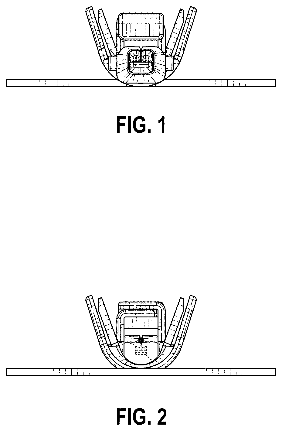
FIG. 1 is a front elevational view of a connector terminal showing a first embodiment of our new design;
FIG. 2 is a rear elevational view thereof;
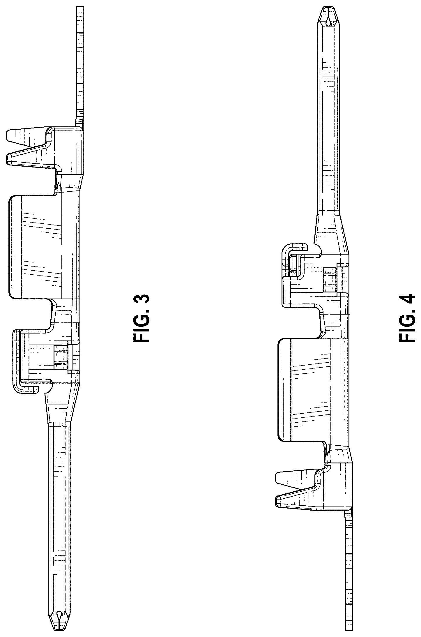
FIG. 3 is a right side elevational view thereof;
FIG. 4 is a left side elevational view thereof;
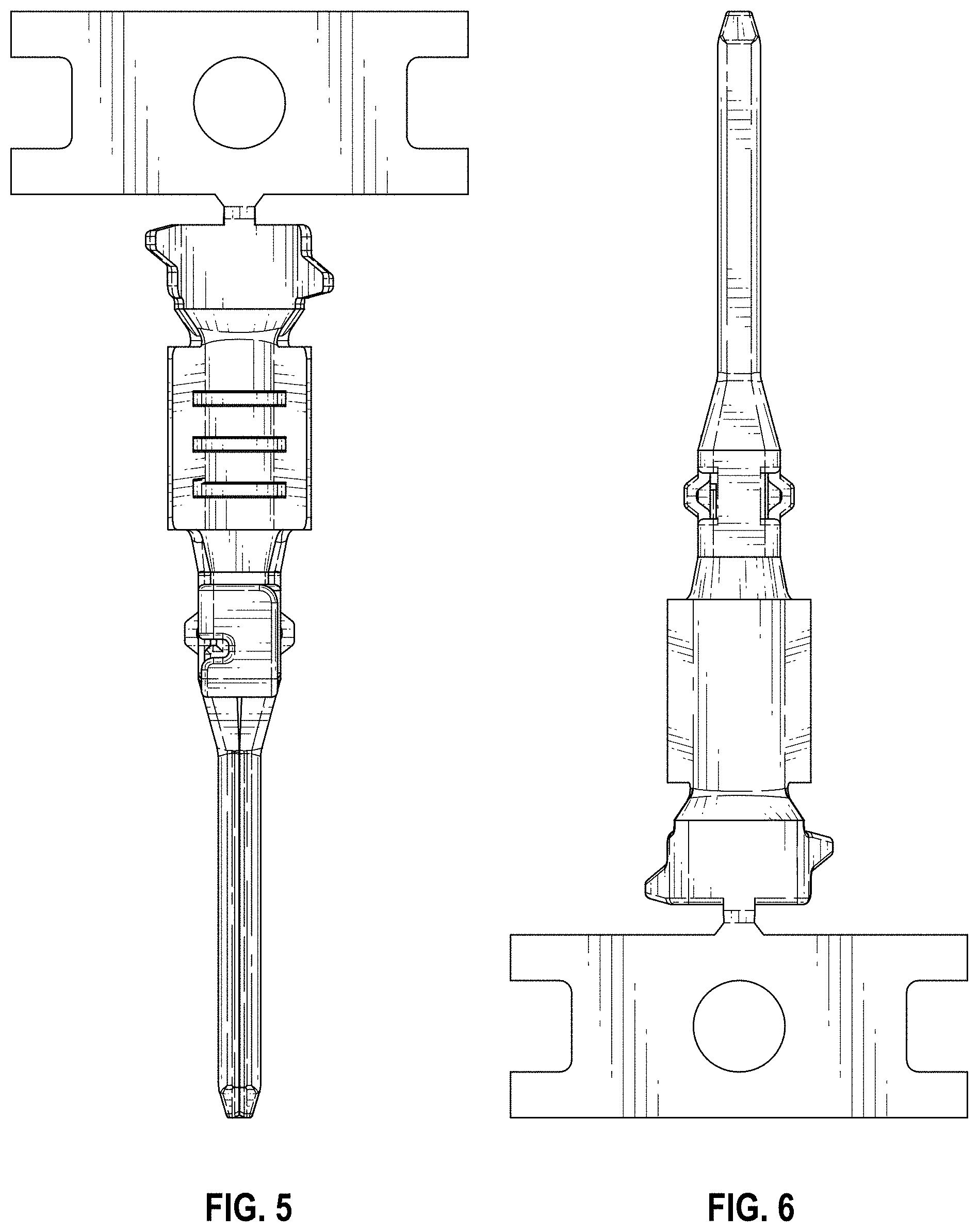
FIG. 5 is a top plan view thereof;
FIG. 6 is a bottom plan view thereof;
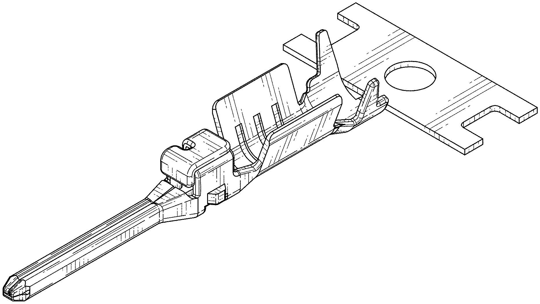
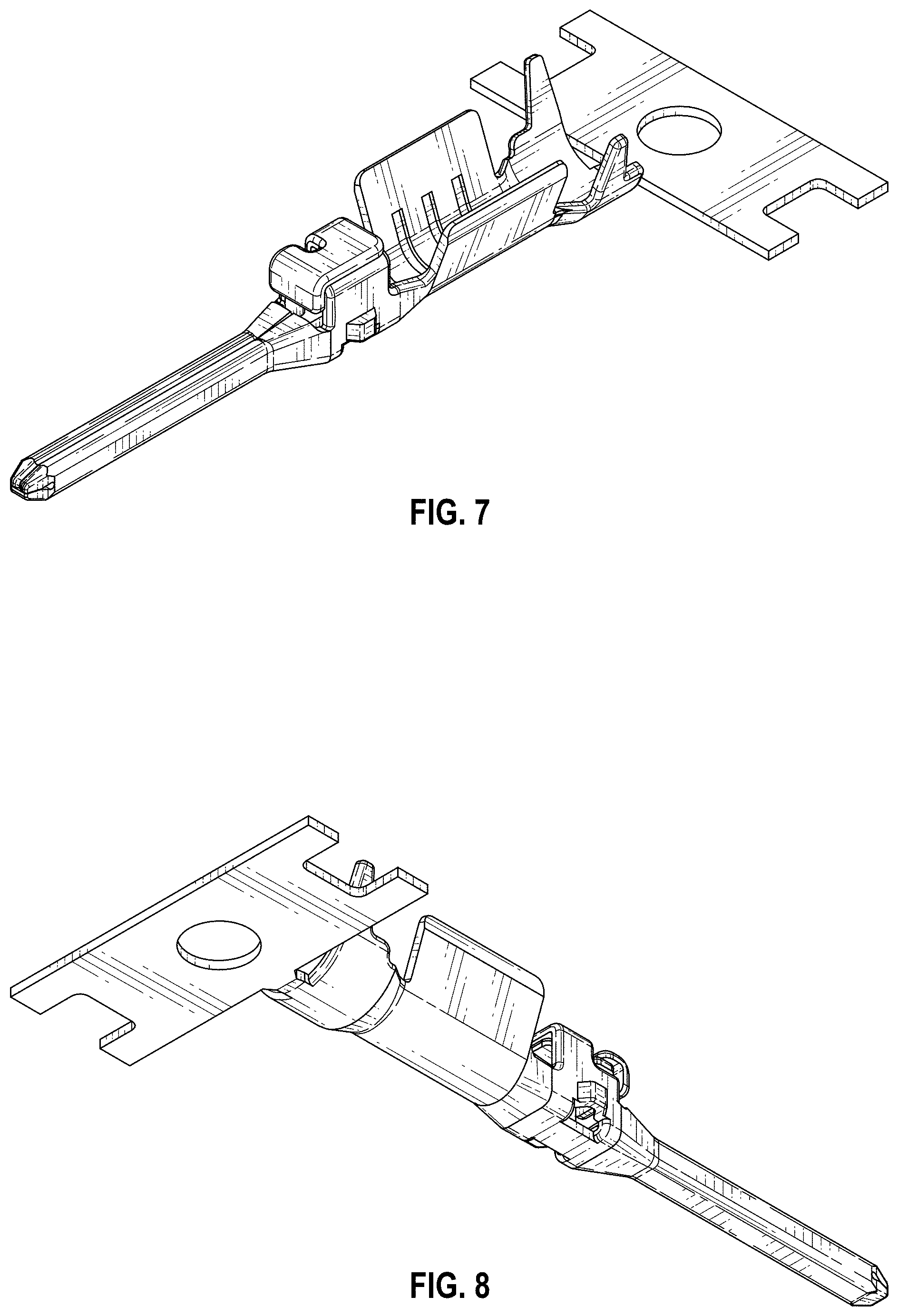
FIG. 7 is a perspective view showing a front, top and right side thereof;
FIG. 8 is a perspective view showing a rear, bottom and left side thereof;
FIG. 9 is a perspective view showing a front, right and bottom side thereof;
FIG. 10 is a perspective view showing a rear, left and top side thereof;
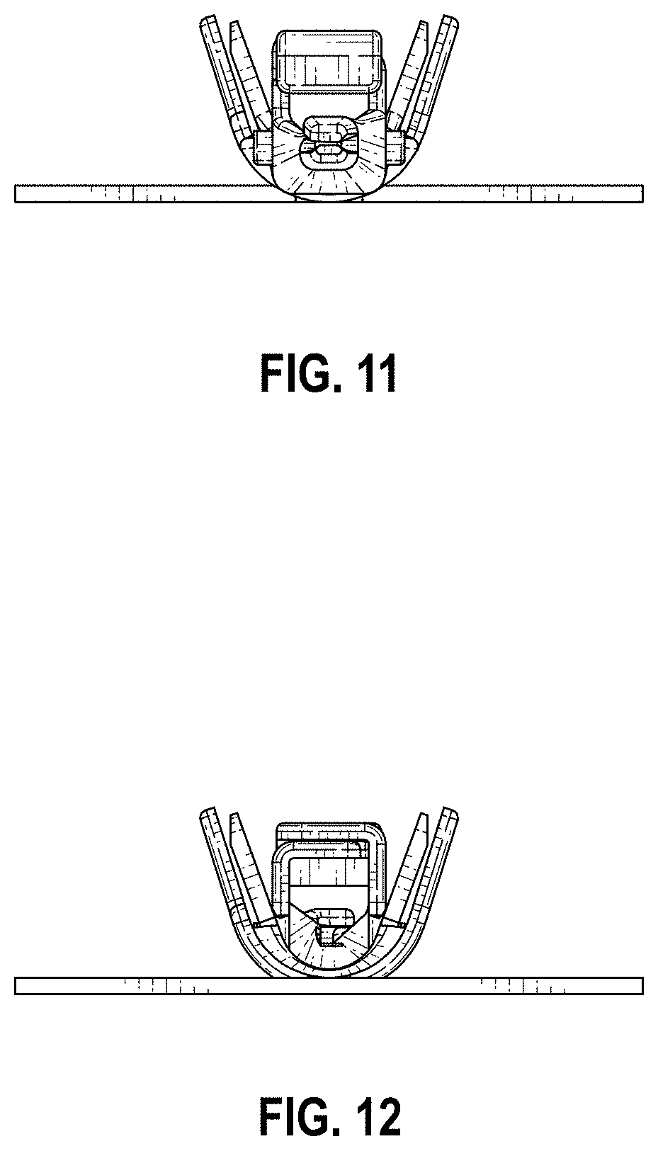
FIG. 11 is a front elevational view of a connector terminal showing a second embodiment of our new design;
FIG. 12 is a rear elevational view thereof;
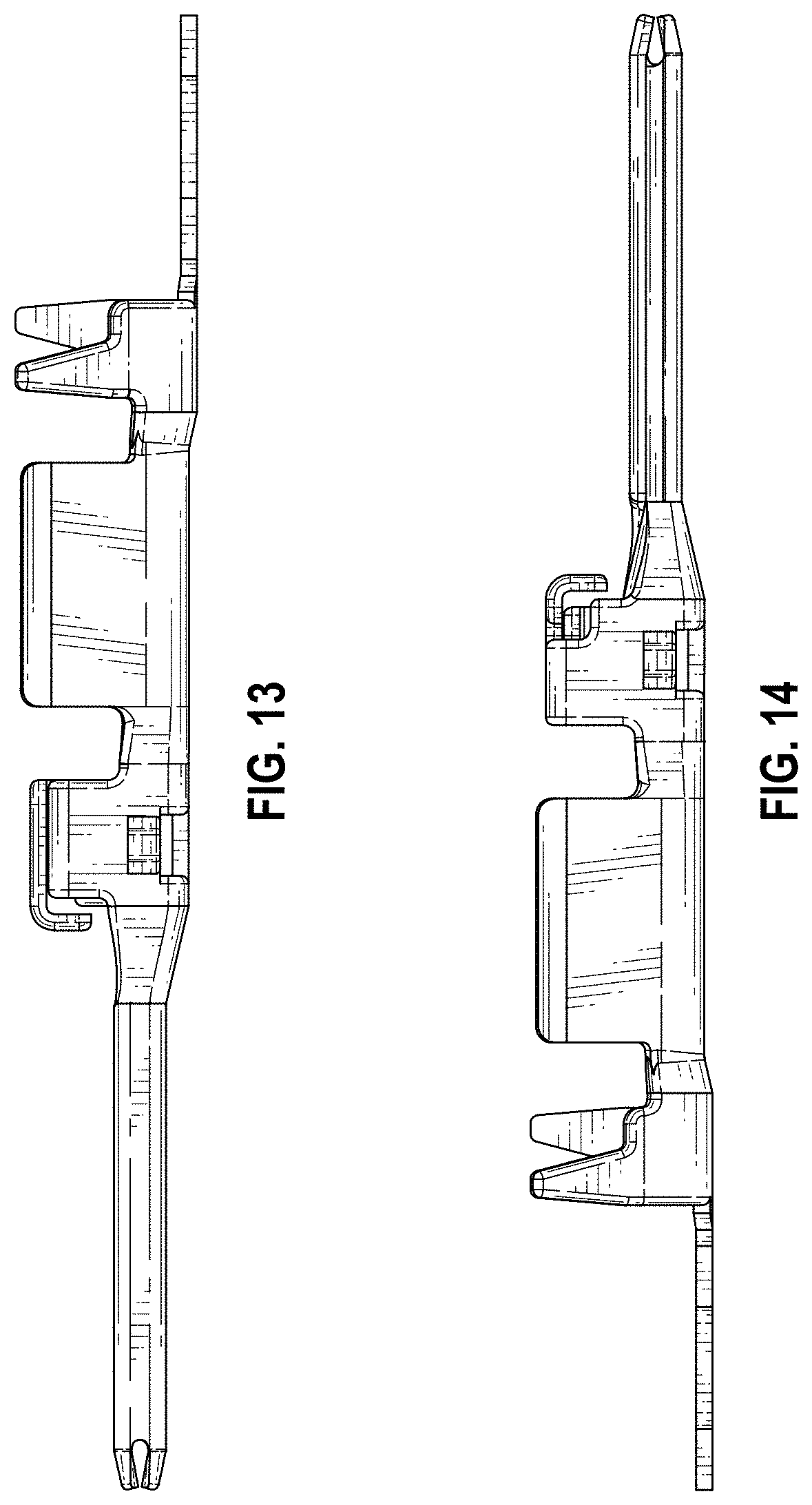
FIG. 13 is a right side elevational view thereof;
FIG. 14 is a left side elevational view thereof;
FIG. 15 is a top plan view thereof;
FIG. 16 is a bottom plan view thereof;
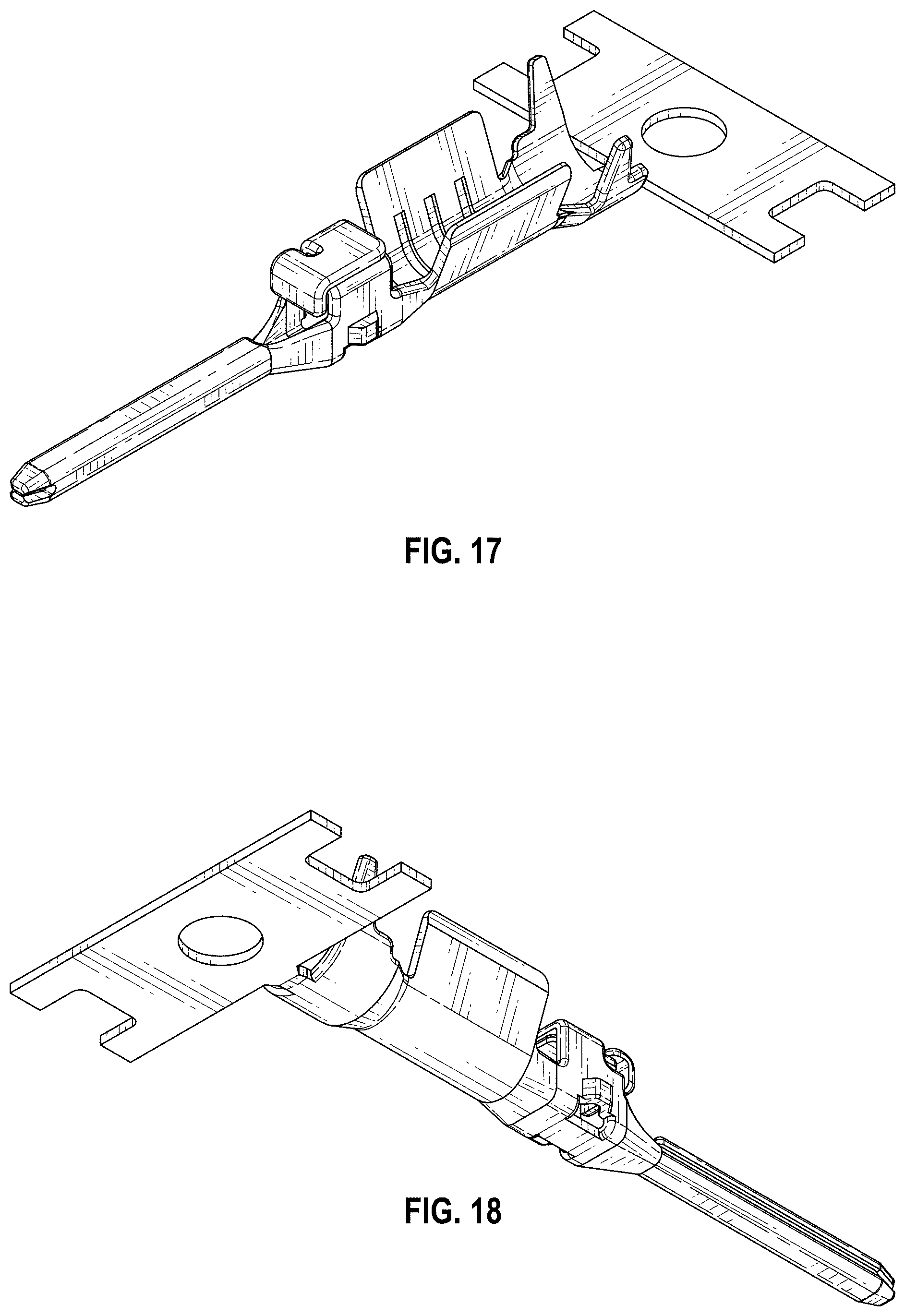
FIG. 17 is a perspective view showing a front, top and right side thereof;
FIG. 18 is a perspective view showing a rear, bottom and left side thereof;
FIG. 19 is a perspective view showing a front, right and bottom side thereof;
FIG. 20 is a perspective view showing a rear, left and top side thereof;
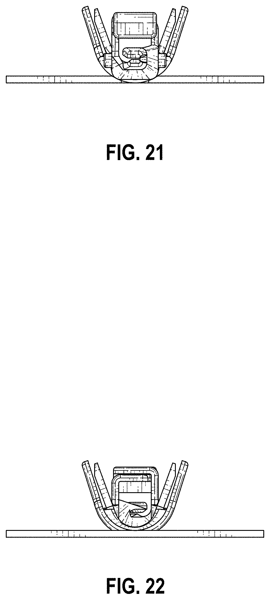
FIG. 21 is a front elevational view of a connector terminal showing a third embodiment of our new design;
FIG. 22 is a rear elevational view thereof;
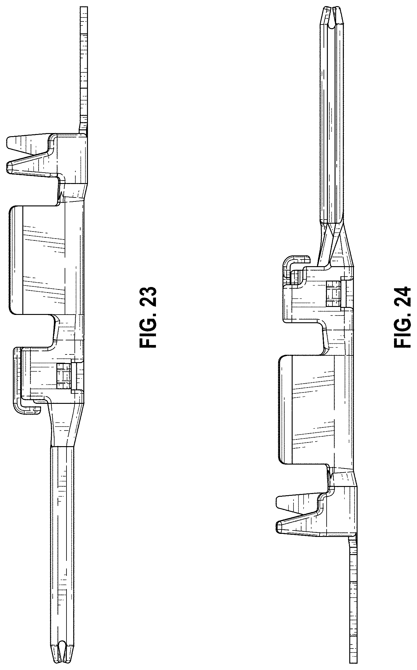
FIG. 23 is a right side elevational view thereof;
FIG. 24 is a left side elevational view thereof;
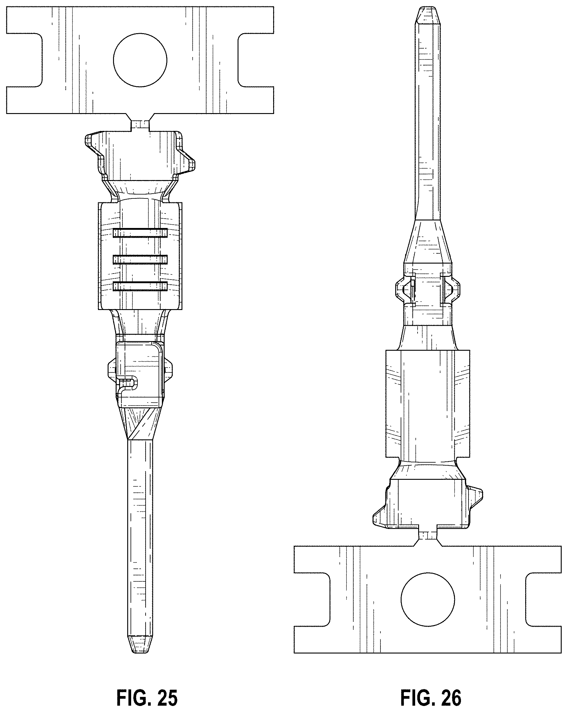
FIG. 25 is a top plan view thereof;
FIG. 26 is a bottom plan view thereof;
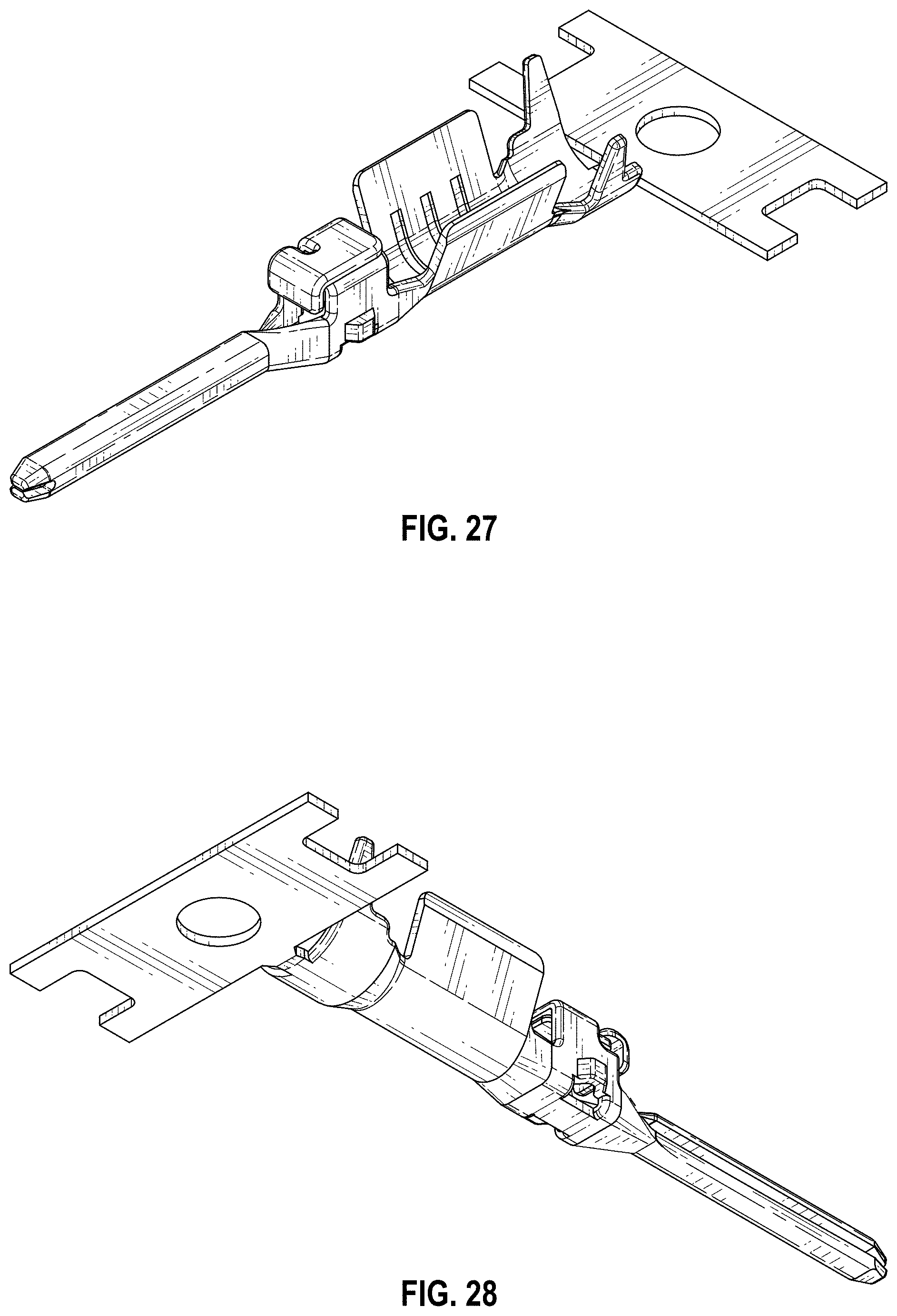
FIG. 27 is a perspective view showing a front, top and right side thereof;
FIG. 28 is a perspective view showing a rear, bottom and left side thereof;
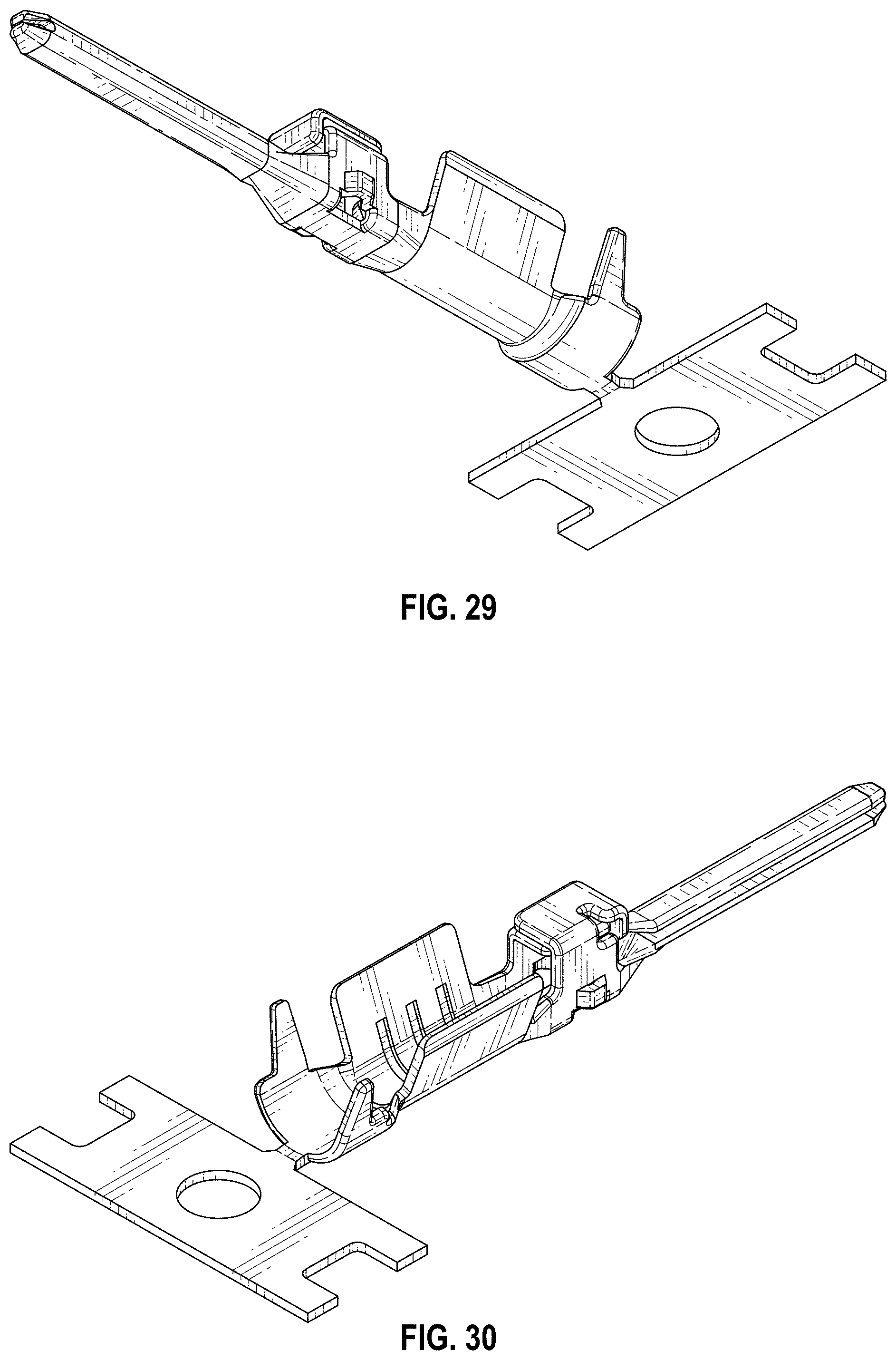
FIG. 29 is a perspective view showing a front, right and bottom side thereof; and,
FIG. 30 is a perspective view showing a rear, left and top side thereof.
The broken line showing of the connector terminal is for the purpose of illustrating portions of the article and forms no part of the claimed design.
* * * * *
D00000
D00001
D00002
D00003
D00004
D00005
D00006
D00007
D00008
D00009
D00010
D00011
D00012
D00013
D00014
D00015
XML
uspto.report is an independent third-party trademark research tool that is not affiliated, endorsed, or sponsored by the United States Patent and Trademark Office (USPTO) or any other governmental organization. The information provided by uspto.report is based on publicly available data at the time of writing and is intended for informational purposes only.
While we strive to provide accurate and up-to-date information, we do not guarantee the accuracy, completeness, reliability, or suitability of the information displayed on this site. The use of this site is at your own risk. Any reliance you place on such information is therefore strictly at your own risk.
All official trademark data, including owner information, should be verified by visiting the official USPTO website at www.uspto.gov. This site is not intended to replace professional legal advice and should not be used as a substitute for consulting with a legal professional who is knowledgeable about trademark law.