Light emitting diode
Kuriki , et al. Sep
U.S. patent number D895,559 [Application Number D/685,330] was granted by the patent office on 2020-09-08 for light emitting diode. This patent grant is currently assigned to CITIZEN ELECTRONICS CO., LTD., CITIZEN WATCH CO., LTD. The grantee listed for this patent is CITIZEN ELECTRONICS CO., LTD., CITIZEN WATCH CO., LTD.. Invention is credited to Shingo Kuriki, Kazuki Matsumura, Yuji Omori, Masahiro Watanabe.


View All Diagrams
| United States Patent | D895,559 |
| Kuriki , et al. | September 8, 2020 |
Light emitting diode
Claims
CLAIM The ornamental design for a light emitting diode, as shown and described.
| Inventors: | Kuriki; Shingo (Yamanashi, JP), Watanabe; Masahiro (Yamanashi, JP), Matsumura; Kazuki (Fuefuki, JP), Omori; Yuji (Yamanashi, JP) | ||||||||||
|---|---|---|---|---|---|---|---|---|---|---|---|
| Applicant: |
|
||||||||||
| Assignee: | CITIZEN ELECTRONICS CO., LTD.
(Fujiyoshida-Shi, JP) CITIZEN WATCH CO., LTD (Tokyo, JP) |
||||||||||
| Appl. No.: | D/685,330 | ||||||||||
| Filed: | March 27, 2019 |
Foreign Application Priority Data
| Jan 15, 2019 [JP] | 2019-000628 | |||
| Jan 15, 2019 [JP] | 2019-000630 | |||
| Jan 15, 2019 [JP] | 2019-000631 | |||
| Jan 15, 2019 [JP] | 2019-000632 | |||
| Current U.S. Class: | D13/180 |
| Current International Class: | 1303 |
| Field of Search: | ;D13/180 ;D24/1,2 |
References Cited [Referenced By]
U.S. Patent Documents
| D405426 | February 1999 | Yamaoka |
| 6520669 | February 2003 | Chen |
| D489142 | April 2004 | Froech |
| D494286 | August 2004 | Matsui |
| D494288 | August 2004 | Matsui |
| D508573 | August 2005 | Matsui |
| D514530 | February 2006 | Matsui |
| D528994 | September 2006 | Matsui |
| D528996 | September 2006 | Egawa |
| D562473 | February 2008 | Matsui |
| D608740 | January 2010 | Lu |
| D636925 | April 2011 | Kawagoe |
| D639498 | June 2011 | Kawagoe |
| D674523 | January 2013 | Kaffash |
| D675347 | January 2013 | Wollard |
| 8440500 | May 2013 | Su |
| D700585 | March 2014 | Takeda et al. |
| D707192 | June 2014 | Hussell |
| D744156 | November 2015 | Kjaergaard Toft |
| D751046 | March 2016 | Kuriki |
| D778246 | February 2017 | Kuriki |
| D786809 | May 2017 | Kuriki |
| 2008/0112162 | May 2008 | Chan |
| 2012/0056232 | March 2012 | Fujimoto |
| 2014/0138715 | May 2014 | Zhang |
| 2014/0291706 | October 2014 | Lin |
| 2015/0311414 | October 2015 | Lin |
| 2015/0338041 | November 2015 | Wimmer |
| 2017/0092804 | March 2017 | Peng |
| 2017/0103966 | April 2017 | Choi |
| 2017/0279015 | September 2017 | Ryu |
| 2018/0094799 | April 2018 | Shan |
| 2019/0097106 | March 2019 | Ditzel |
Other References
|
Masahiro Watanabe et al., Design U.S. Appl. No. 29/685,304, filed Mar. 27, 2019, not published. cited by applicant . Masahiro Watanabe et al., Design U.S. Appl. No. 29/685,314, filed Mar. 27, 2019, not published. cited by applicant. |
Primary Examiner: Sikder; Selina
Attorney, Agent or Firm: Procopio, Cory, Hargreaves & Savitch LLP
Description
FIG. 1 is a top plan view of a light emitting diode showing our new design;
FIG. 2 is a bottom plan view thereof;
FIG. 3 is a front elevational view thereof;
FIG. 4 is a rear elevational view thereof;
FIG. 5 is a left side elevational view thereof;
FIG. 6 is a right side elevational view thereof;
FIG. 7 is a cross-sectional view thereof taken along the lines 7-7 and 7'-7' in FIG. 1;
FIG. 8 is a top plan view of the second embodiment of a light emitting diode showing our new design;
FIG. 9 is a bottom plan view thereof;
FIG. 10 is a front elevational view thereof;
FIG. 11 is a rear elevational view thereof;
FIG. 12 is a left side elevational view thereof;
FIG. 13 is a right side elevational view thereof;
FIG. 14 is a cross-sectional view thereof taken along the lines 14-14 and 14'-14' in FIG. 8;
FIG. 15 is a top plan view of the third embodiment of a light emitting diode showing our new design;
FIG. 16 is a bottom plan view thereof;
FIG. 17 is a front elevational view thereof;
FIG. 18 is a rear elevational view thereof;
FIG. 19 is a left side elevational view thereof;
FIG. 20 is a right side elevational view thereof;
FIG. 21 is a cross-sectional view thereof taken along the lines 21-21 and 21'-21' in FIG. 15;
FIG. 22 is a top plan view of the fourth embodiment of a light emitting diode showing our new design;
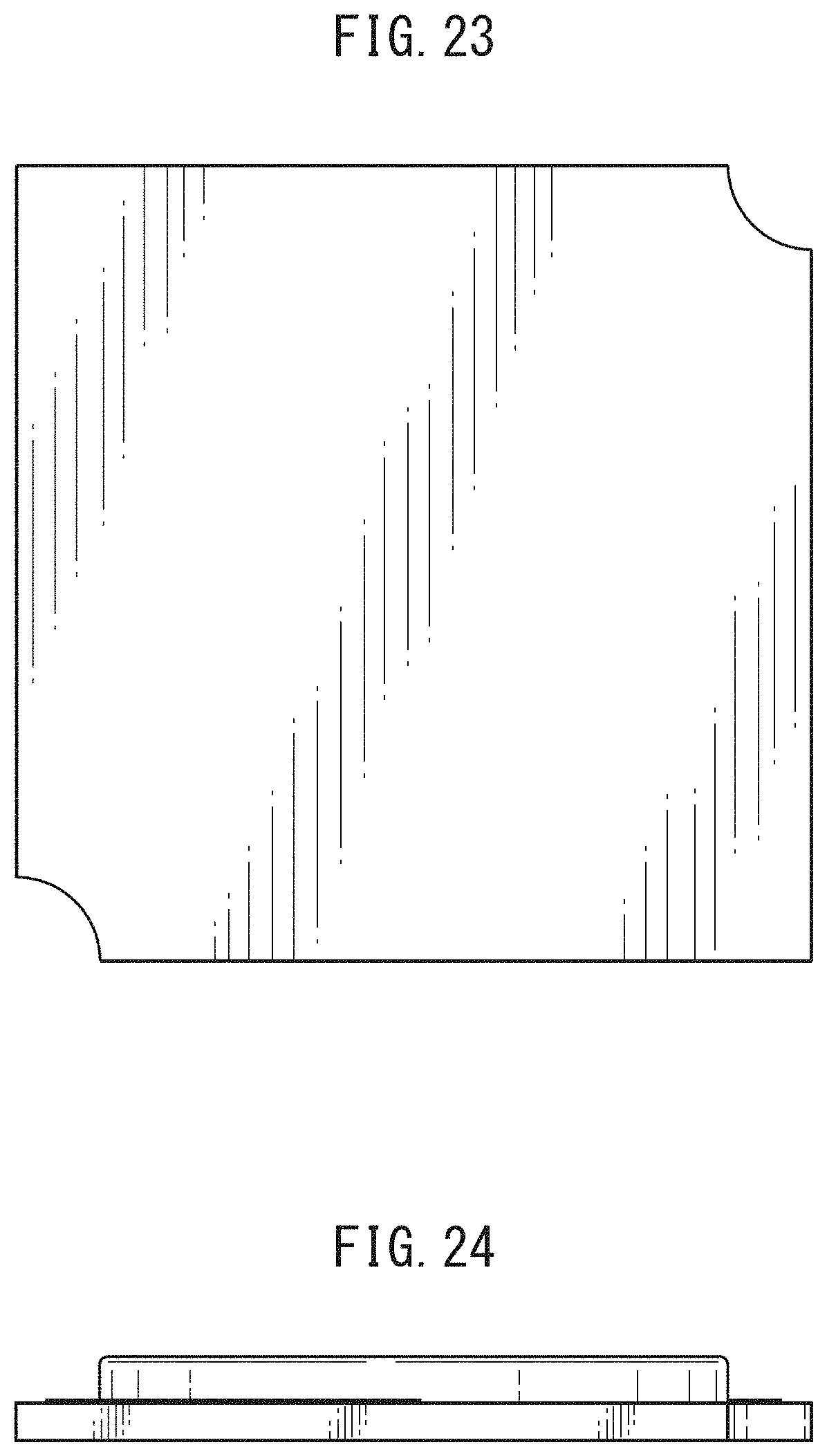
FIG. 23 is a bottom plan view thereof;
FIG. 24 is a front elevational view thereof;
FIG. 25 is a rear elevational view thereof;
FIG. 26 is a left side elevational view thereof;
FIG. 27 is a right side elevational view thereof; and,
FIG. 28 is a cross-sectional view thereof taken along the lines 28-28 and 28'-28' in FIG. 22.
The broken lines shown in FIGS. 1, 7, 8, 15, 21 and 22 are for illustrative purposes only and form no part of the claimed design.
* * * * *
D00000
D00001
D00002
D00003
D00004
D00005
D00006
D00007
D00008
D00009
D00010
D00011
D00012

D00013

D00014
D00015

D00016

XML
uspto.report is an independent third-party trademark research tool that is not affiliated, endorsed, or sponsored by the United States Patent and Trademark Office (USPTO) or any other governmental organization. The information provided by uspto.report is based on publicly available data at the time of writing and is intended for informational purposes only.
While we strive to provide accurate and up-to-date information, we do not guarantee the accuracy, completeness, reliability, or suitability of the information displayed on this site. The use of this site is at your own risk. Any reliance you place on such information is therefore strictly at your own risk.
All official trademark data, including owner information, should be verified by visiting the official USPTO website at www.uspto.gov. This site is not intended to replace professional legal advice and should not be used as a substitute for consulting with a legal professional who is knowledgeable about trademark law.