Connector assembly
Bowron Nov
U.S. patent number D867,108 [Application Number D/568,900] was granted by the patent office on 2019-11-19 for connector assembly. This patent grant is currently assigned to Vector Bloc, Corp.. The grantee listed for this patent is Vectorbloc Corp.. Invention is credited to Julian Bowron.


| United States Patent | D867,108 |
| Bowron | November 19, 2019 |
Connector assembly
Claims
CLAIM The ornamental design for a connector assembly, as shown and described.
| Inventors: | Bowron; Julian (Toronto, CA) | ||||||||||
|---|---|---|---|---|---|---|---|---|---|---|---|
| Applicant: |
|
||||||||||
| Assignee: | Vector Bloc, Corp. (Toronto,
CA) |
||||||||||
| Appl. No.: | D/568,900 | ||||||||||
| Filed: | June 22, 2016 |
Foreign Application Priority Data
| Mar 18, 2016 [CA] | 167636 | |||
| Current U.S. Class: | D8/354 |
| Current International Class: | 0805 |
| Field of Search: | ;D8/48,71,315-322,354-355,378-381,400-499 ;D12/420,223 ;D25/119-125,199 |
References Cited [Referenced By]
U.S. Patent Documents
| 946423 | January 1910 | Connaty |
| 2037736 | April 1936 | Payne et al. |
| 3205611 | September 1965 | Onanian |
| 3416270 | December 1968 | McHugh |
| 3824750 | June 1974 | Antoniou |
| 3973855 | August 1976 | Florence |
| 4003144 | January 1977 | Maddestra |
| D248447 | July 1978 | Hornung |
| D258194 | February 1981 | Stanley |
| 4758111 | July 1988 | Vitta |
| 5127759 | July 1992 | Orbom |
| 5259685 | November 1993 | Wolf |
| D357544 | April 1995 | Spransy |
| 5414918 | May 1995 | Pearson |
| 5440844 | August 1995 | Zinser, Jr. |
| 5516225 | May 1996 | Kvols |
| 5590974 | January 1997 | Yang |
| 5605410 | February 1997 | Pantev |
| 5727358 | March 1998 | Hayashi et al. |
| 5816011 | October 1998 | Kuramoto |
| 5820289 | October 1998 | Kern et al. |
| 5904437 | May 1999 | Allen |
| 5921049 | July 1999 | Sugiyama |
| 6062761 | May 2000 | Allen |
| 6092849 | July 2000 | Zambelli et al. |
| 6247869 | June 2001 | Lichvar |
| 6332657 | December 2001 | Fischer |
| 6390719 | May 2002 | Chan |
| 6974276 | December 2005 | Kirchner et al. |
| 7503623 | March 2009 | Favaretto |
| D622865 | August 2010 | Bajrami |
| 7882388 | February 2011 | Bramante |
| 7883288 | February 2011 | Jorna |
| 7941985 | May 2011 | Simmons |
| 8176703 | May 2012 | Tremacchi |
| 9121433 | September 2015 | Bacon |
| D756202 | May 2016 | Leduc |
| 9334642 | May 2016 | Tanaka et al. |
| 9458619 | October 2016 | Bowron |
| 10036156 | July 2018 | Macdonald et al. |
| 2002/0007614 | January 2002 | Katayama et al. |
| 2006/0112657 | June 2006 | Abbot-Wilcox |
| 2009/0307994 | December 2009 | Cathcart |
| 2011/0219708 | September 2011 | Ohnishi et al. |
| 2011/0286121 | November 2011 | Werner et al. |
| 2011/0308063 | December 2011 | Feeleus |
| 2013/0045042 | February 2013 | Ohlson |
| 2013/0306808 | November 2013 | Huang |
| 2014/0286695 | September 2014 | Jocham et al. |
| 2014/0294500 | October 2014 | Schaff et al. |
| 2015/0184369 | July 2015 | Carless |
| 2016/0002909 | January 2016 | Bowron |
| 2017/0002559 | January 2017 | Bowron et al. |
| 2018/0216336 | August 2018 | Macdonald et al. |
| 2019/0044753 | February 2019 | Neeld |
| 2019/0078321 | March 2019 | Bowron |
| 2744074 | Dec 2011 | CA | |||
| 231689 | Jun 2000 | CN | |||
| 101575876 | Nov 2009 | CN | |||
| 101680227 | Mar 2010 | CN | |||
| 202559534 | Nov 2012 | CN | |||
| 203834666 | Sep 2014 | CN | |||
| 249 688 | Sep 1987 | DE | |||
| 195 17 785 | Nov 1996 | DE | |||
| 697 04 916 | Nov 2001 | DE | |||
| 0761 895 | Mar 1997 | EP | |||
| 0761895 | Mar 1997 | EP | |||
| 2759648 | Jul 2014 | EP | |||
| 2300432 | Nov 1996 | GB | |||
| 2554967 | Apr 2018 | GB | |||
| H03233042 | Oct 1991 | JP | |||
| H07180221 | Jul 1995 | JP | |||
| H07180228 | Jul 1995 | JP | |||
| 3014203 | Aug 1995 | JP | |||
| H07243239 | Sep 1995 | JP | |||
| H09194179 | Jul 1997 | JP | |||
| 2004270438 | Sep 2004 | JP | |||
| 2005139623 | Jun 2005 | JP | |||
| 2006063787 | Mar 2006 | JP | |||
| 2009024419 | Feb 2009 | JP | |||
| 2013167131 | Aug 2013 | JP | |||
| 2013245501 | Dec 2013 | JP | |||
| 100923637 | Oct 2009 | KR | |||
| 20110053101 | May 2011 | KR | |||
| 294752 | Jan 1997 | TW | |||
| 03069083 | Aug 2003 | WO | |||
| 2004035952 | Apr 2004 | WO | |||
| 2006/096997 | Sep 2006 | WO | |||
| 2006096997 | Sep 2006 | WO | |||
| 2006122372 | Nov 2006 | WO | |||
| 2007144913 | Dec 2007 | WO | |||
| 2010035816 | Apr 2010 | WO | |||
| 2012083391 | Jun 2012 | WO | |||
| 2012/129601 | Oct 2012 | WO | |||
| 2012129601 | Oct 2012 | WO | |||
| 2014127472 | Aug 2014 | WO | |||
| 2015164975 | Nov 2015 | WO | |||
| 2017027965 | Feb 2017 | WO | |||
Other References
|
Written Opinion issued by the Intellectual Property Office of Singapore for International Application No. PCT/CA2014/050110 dated May 2, 2016, 5 pages. cited by applicant . PCT International Search Report for International Application No. PCT/CA2014/050110 dated May 5, 2014, 4 pages. cited by applicant . Written Opinion issued by the Canadian Intellectual Property Office for International Application No. PCT/CA2016/050954 dated Oct. 14, 2016, 8 pages. cited by applicant . International Search Report for International Application No. PCT/CA2016/050954 dated Oct. 14, 2016, 5 pages. cited by applicant . Chinese Office Action dated Jun. 19, 2018. cited by applicant . Office Action issued against corresponding Japanese Patent Application No. JP2015-558313 dated Mar. 6, 2018. cited by applicant . Extended European Search Report issued against corresponding International Application PCT/CA2015050369 dated Nov. 20, 2017. cited by applicant . Information on Search Strategy. cited by applicant . Extended European Search Report issued against Intemational Application No. PCT/CA2016050954 dated Feb. 14, 2019. cited by applicant . Extended European Search Report issued against International Application No. PCT/CA2014050110 dated Jan. 20, 2017. cited by applicant . Office Action issued against corresponding Japanese Application 2017-508717 dated Feb. 26, 2019. cited by applicant . First Office Action and Search Report for corresponding Chinese Patent Application No. 201680027827.9 dated Apr. 15, 2019. cited by applicant . Written Opinion of the International Searching Authority for PCT/CA2016050434 dated Jun. 23, 2016. cited by applicant . Written Opinion of the International Searching Authority for PCT/CA2015050369 dated Jul. 14, 2015. cited by applicant . Office Action issued against corresponding Chinese Application No. 201480022662.7 dated Jul. 18, 2017. cited by applicant. |
Primary Examiner: Fox; Barbara
Assistant Examiner: Reed; Kristin E
Attorney, Agent or Firm: Fitch, Even, Tabin & Flannery
Description
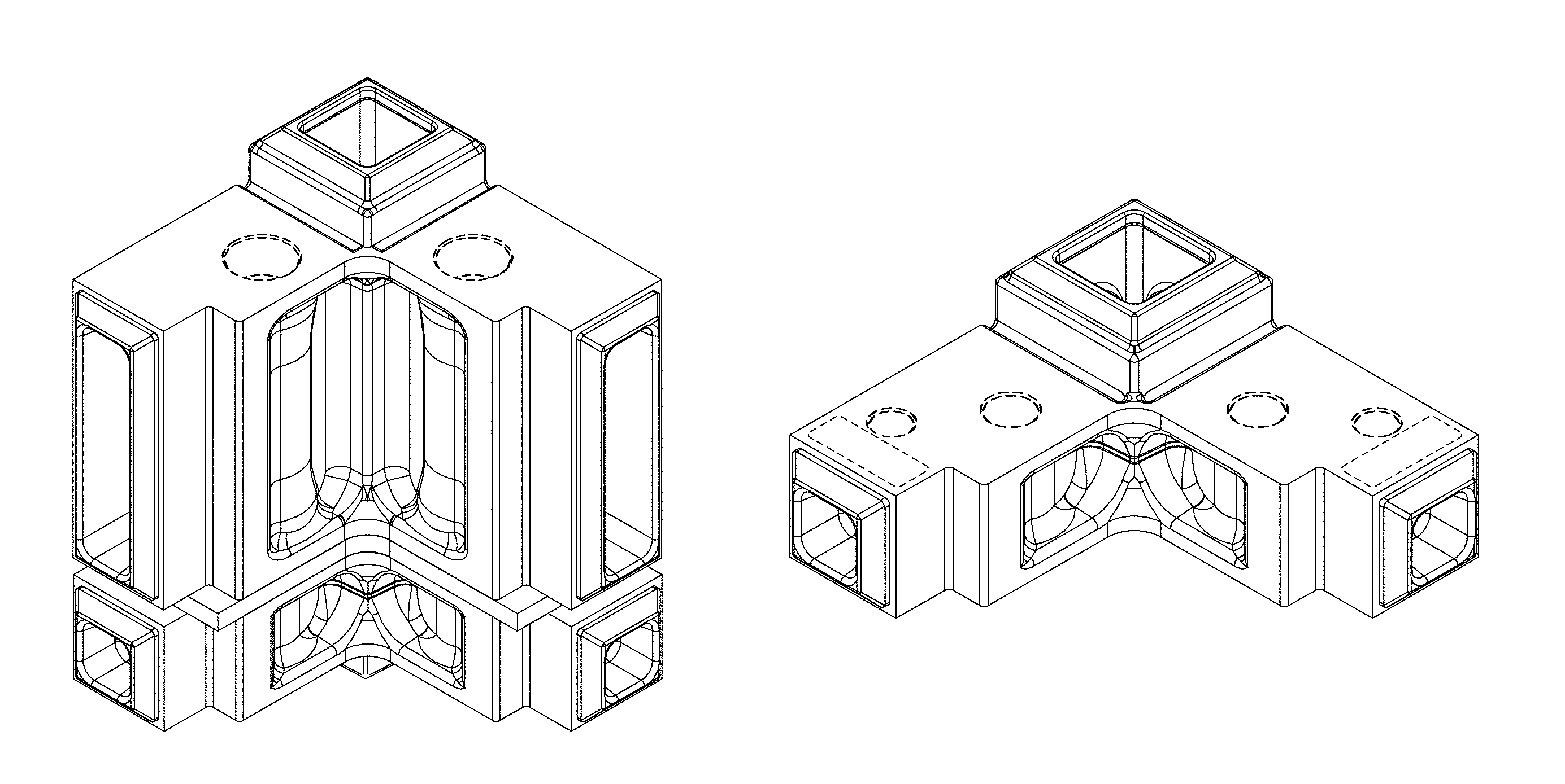
FIG. 1 is a perspective view of a connector assembly showing my new design;
FIG. 2 is a front view of the connector assembly of FIG. 1;
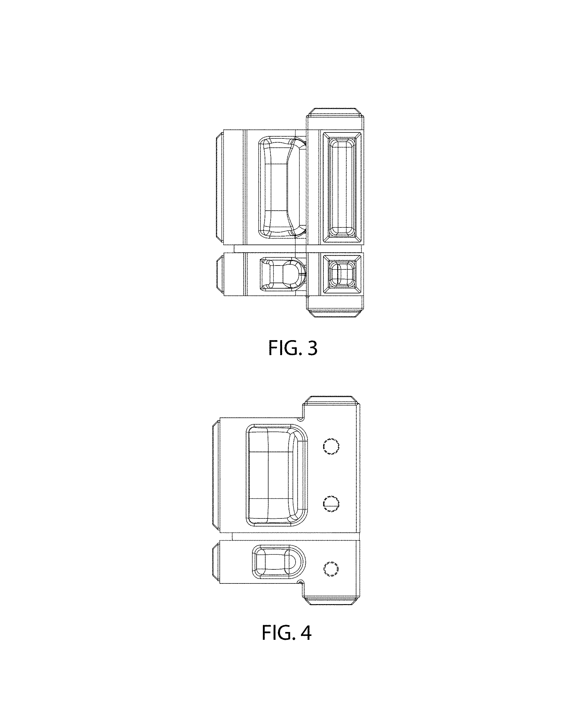
FIG. 3 is a right side view of the connector assembly of FIG. 1;
FIG. 4 is a back side view of the connector assembly of FIG. 1;
FIG. 5 is a left side view of the connector assembly of FIG. 1;
FIG. 6 is a top view of the connector assembly of FIG. 1;
FIG. 7 is a bottom view of the connector assembly of FIG. 1;
FIG. 8 is a perspective view of the top corner connector portion of the connector assembly of FIG. 1, the top corner connector portion being shown separately to show aspects of the design that are not visible when the top corner connector portion is combined with other portions of the design;
FIG. 9 is a top view of the top corner connector portion of FIG. 8;
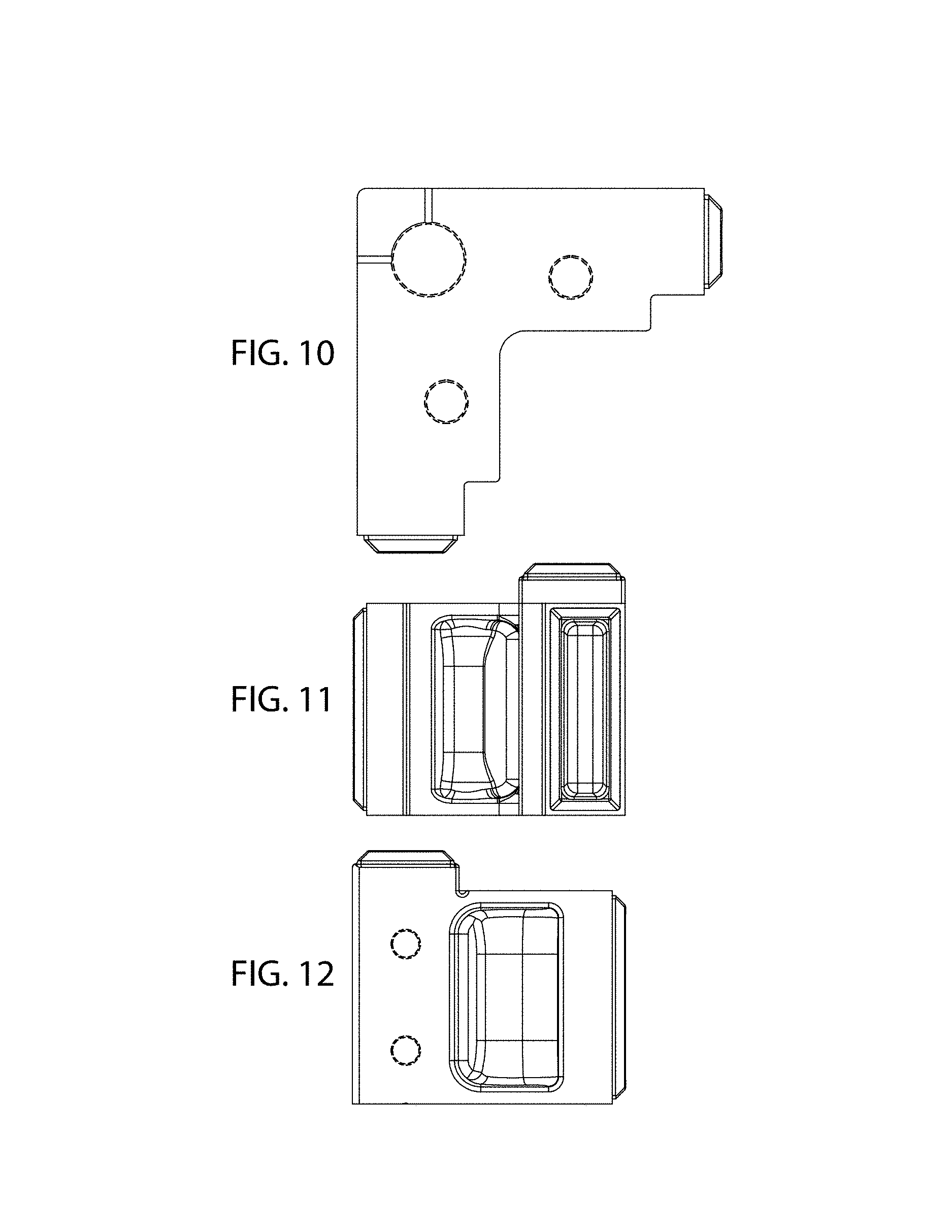
FIG. 10 is a bottom view of the top corner connector portion of FIG. 8;
FIG. 11 is a right side view of the top corner connector portion of FIG. 8;
FIG. 12 is a left side view of the top corner connector portion of FIG. 8;
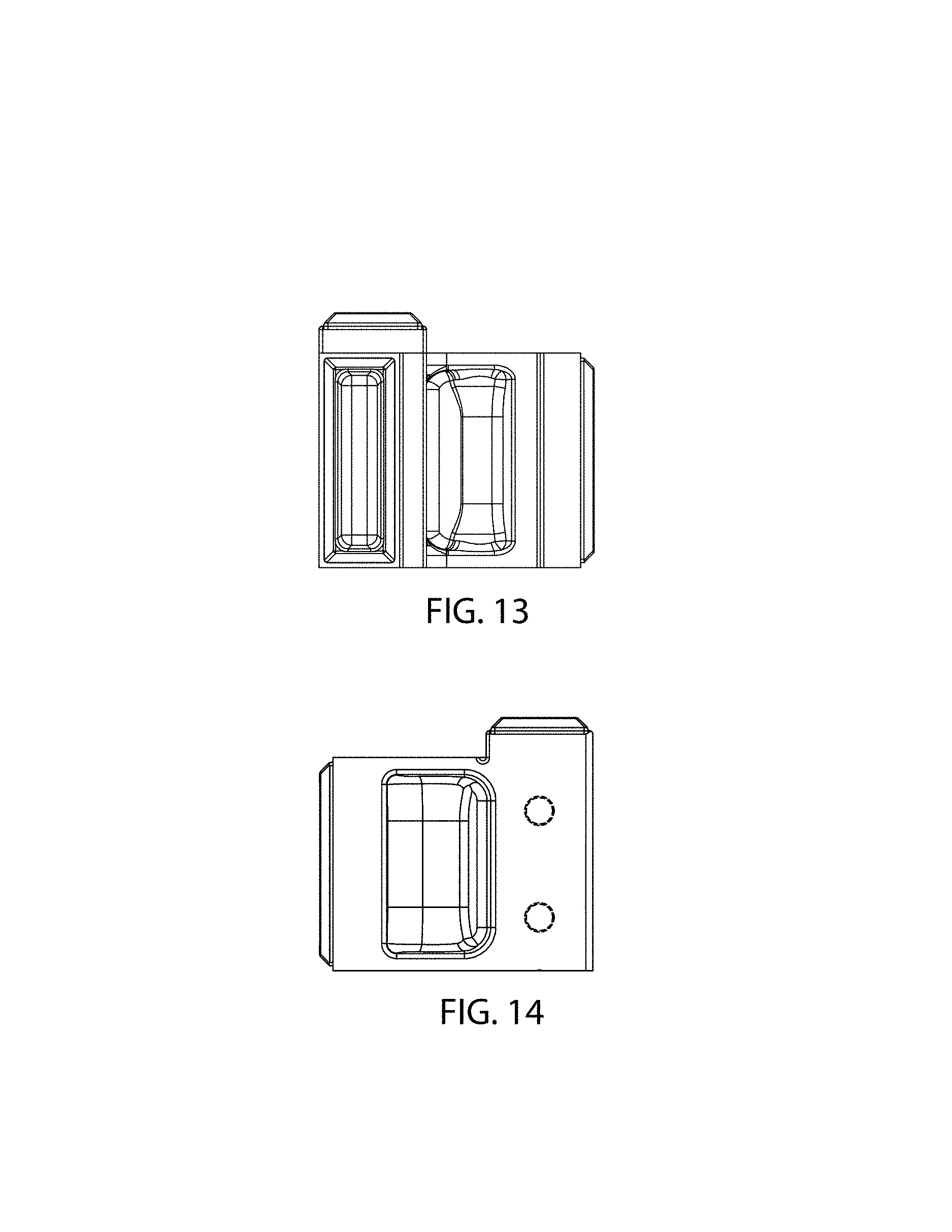
FIG. 13 is a front view of the top corner connector portion of FIG. 8;
FIG. 14 is back side view of the top corner connector portion of FIG. 8;
FIG. 15 is a perspective view of the bottom corner connector portion of the connector assembly of FIG. 1, the bottom corner connector portion being shown separately to show aspects of the design that are not visible when the bottom corner connector portion is combined with other portions of the design;
FIG. 16 is a bottom view of the bottom corner connector portion of FIG. 15;
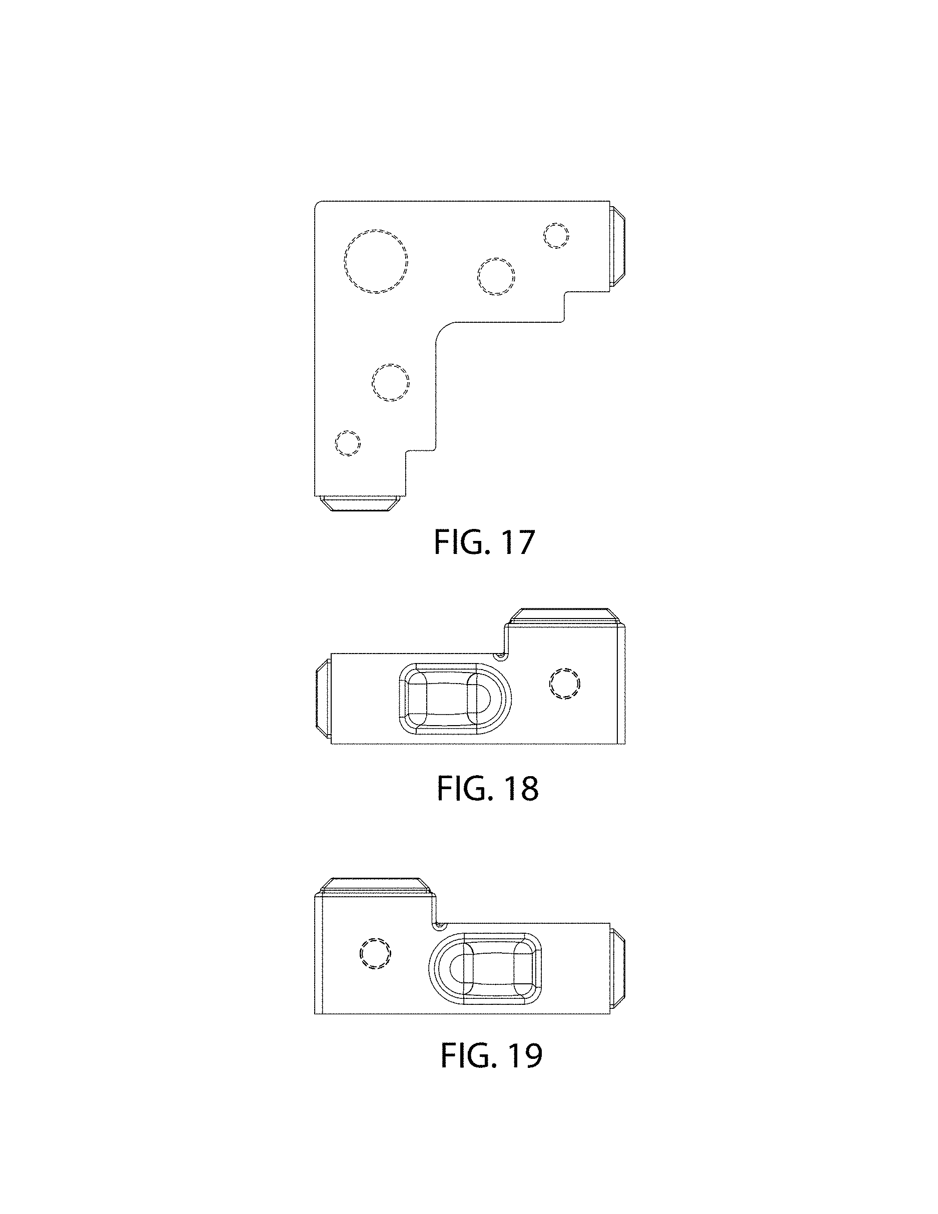
FIG. 17 is a top view of the bottom corner connector portion of FIG. 15;
FIG. 18 is a left side view of the bottom corner connector portion of FIG. 15;
FIG. 19 is a back side view of the bottom corner connector portion of FIG. 15;
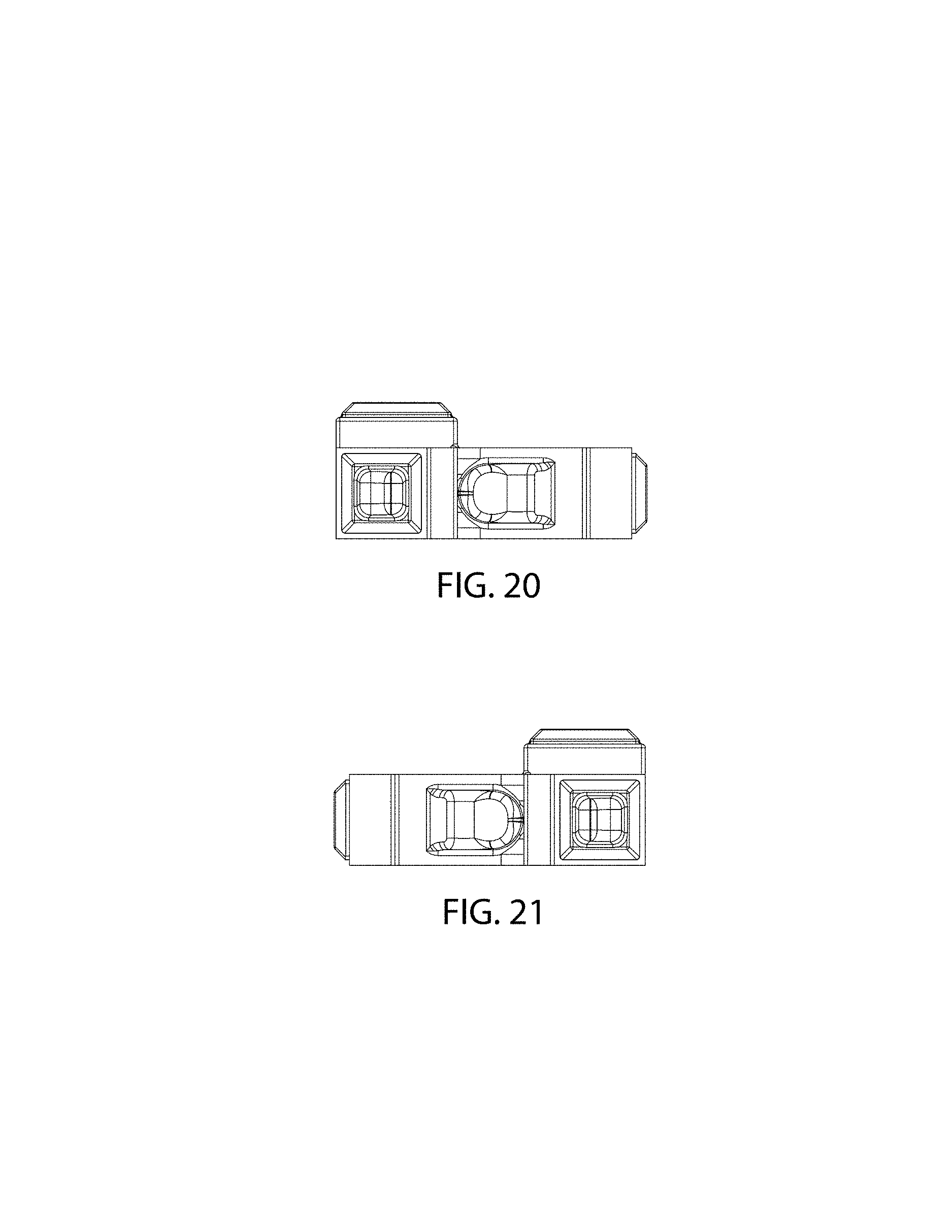
FIG. 20 is a right side view of the bottom corner connector portion of FIG. 15;
FIG. 21 is a front view of the bottom corner connector portion of FIG. 15;
FIG. 22 is a perspective view of the gusset plate corner connector portion of the connector assembly of FIG. 1, the gusset plate corner connector portion being shown separately to show aspects of the design that are not visible when the gusset plate corner connector portion is combined with other portions of the design;
FIG. 23 is a top view of the gusset plate of FIG. 22;
FIG. 24 is a bottom view of the gusset plate of FIG. 22;
FIG. 25 is a left side view of the gusset plate of FIG. 22;
FIG. 26 is a front view of the gusset plate of FIG. 22; and,
FIG. 27 is a right side view of the gusset plate of FIG. 22.
The broken lines in the drawings are for the purpose of illustrating portions of the connector assembly that form no part of the claimed design.
* * * * *
D00000
D00001
D00002
D00003
D00004
D00005
D00006
D00007
D00008
D00009
D00010
XML
uspto.report is an independent third-party trademark research tool that is not affiliated, endorsed, or sponsored by the United States Patent and Trademark Office (USPTO) or any other governmental organization. The information provided by uspto.report is based on publicly available data at the time of writing and is intended for informational purposes only.
While we strive to provide accurate and up-to-date information, we do not guarantee the accuracy, completeness, reliability, or suitability of the information displayed on this site. The use of this site is at your own risk. Any reliance you place on such information is therefore strictly at your own risk.
All official trademark data, including owner information, should be verified by visiting the official USPTO website at www.uspto.gov. This site is not intended to replace professional legal advice and should not be used as a substitute for consulting with a legal professional who is knowledgeable about trademark law.