Western blot processing device housing
Mead , et al. A
U.S. patent number D857,917 [Application Number D/594,454] was granted by the patent office on 2019-08-27 for western blot processing device housing. This patent grant is currently assigned to LIFE TECHNOLOGIES CORPORATION. The grantee listed for this patent is LIFE TECHNOLOGIES CORPORATION. Invention is credited to Kyle Bulloch, Sandro Klein, Xin Mathers, Joshua Mead.


View All Diagrams
| United States Patent | D857,917 |
| Mead , et al. | August 27, 2019 |
Western blot processing device housing
Claims
CLAIM The ornamental design for a western blot processing device housing, as shown and described.
| Inventors: | Mead; Joshua (San Diego, CA), Klein; Sandro (Irvine, CA), Mathers; Xin (Poway, CA), Bulloch; Kyle (San Diego, CA) | ||||||||||
|---|---|---|---|---|---|---|---|---|---|---|---|
| Applicant: |
|
||||||||||
| Assignee: | LIFE TECHNOLOGIES CORPORATION
(Carlsbad, CA) |
||||||||||
| Appl. No.: | D/594,454 | ||||||||||
| Filed: | February 17, 2017 |
Related U.S. Patent Documents
| Application Number | Filing Date | Patent Number | Issue Date | ||
|---|---|---|---|---|---|
| 29526967 | May 14, 2015 | D783178 | |||
| Current U.S. Class: | D24/233; D24/216 |
| Current International Class: | 2401 |
| Field of Search: | ;D24/216-219,231,232,233,107,169,186 ;D10/81 |
References Cited [Referenced By]
U.S. Patent Documents
| 6194160 | February 2001 | Levin |
| D681234 | April 2013 | Benarieh |
| D717968 | November 2014 | Klein |
| D730216 | May 2015 | McLaughlin |
| D731673 | June 2015 | Klein |
| D735883 | August 2015 | Bauer |
| D738527 | September 2015 | Benarieh |
| D748815 | February 2016 | Murray |
| D757295 | May 2016 | Benarieh |
Description
FIG. 1 is an open back lid perspective view of a first embodiment of our new western blot processing device housing.
FIG. 2 is a front view of FIG. 1 of our new western blot processing device housing.
FIG. 3 is a rear view of FIG. 1 of our new western blot processing device housing.
FIG. 4 is a right side view of FIG. 1 of our new western blot processing device housing.
FIG. 5 is a left side view of FIG. 1 of our new western blot processing device housing.
FIG. 6 is a top view of FIG. 1 of our new western blot processing device housing.
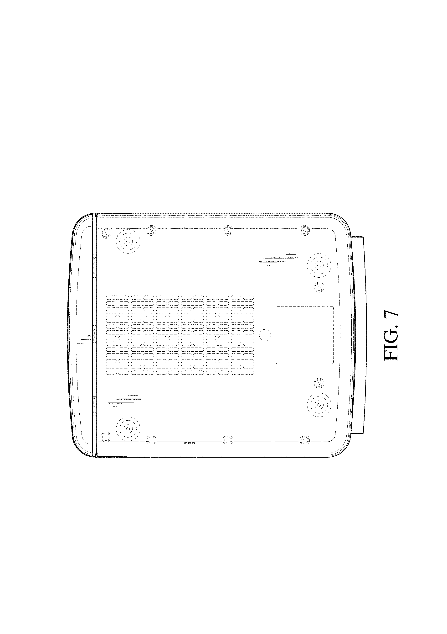
FIG. 7 is a bottom view of FIG. 1 of our new western blot processing device housing.
FIG. 8 is an open back lid perspective view of a second embodiment of our new western blot processing device housing.
FIG. 9 is a front view of FIG. 8 of our new western blot processing device housing.
FIG. 10 is a rear view of FIG. 8 of our new western blot processing device housing.
FIG. 11 is a right side view of FIG. 8 of our new western blot processing device housing.
FIG. 12 is a left side view of FIG. 8 of our new western blot processing device housing.
FIG. 13 is a top view of FIG. 8 of our new western blot processing device housing.
FIG. 14 is a bottom view of FIG. 8 of our new western blot processing device housing.
FIG. 15 is an open lid perspective view of a first embodiment of our new western blot processing device housing.
FIG. 16 is a front view of FIG. 15 of our new western blot processing device housing.
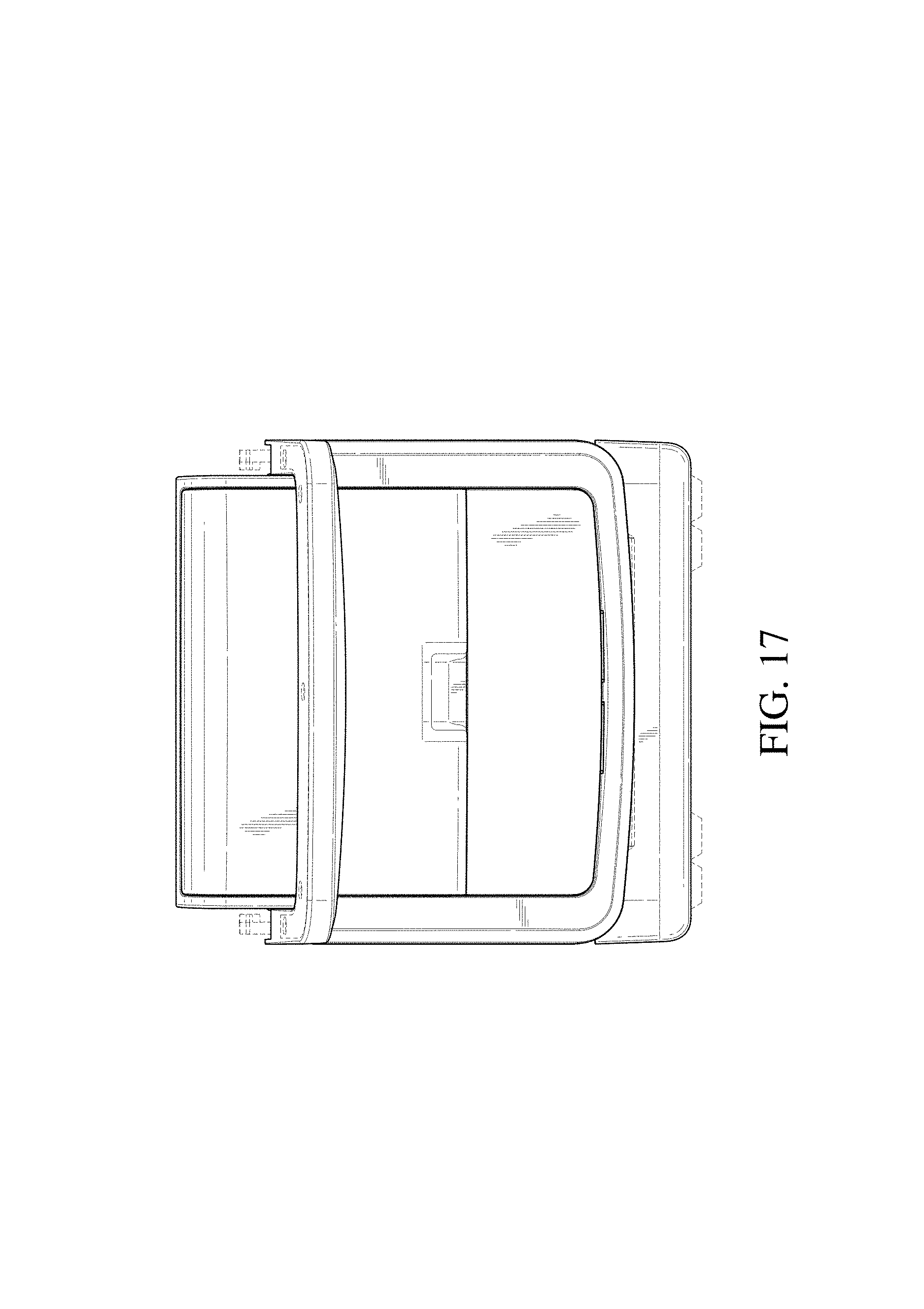
FIG. 17 is a rear view of FIG. 15 of our new western blot processing device housing.
FIG. 18 is a right side view of FIG. 15 of our new western blot processing device housing.
FIG. 19 is a left side view of FIG. 15 of our new western blot processing device housing.
FIG. 20 is a top view of FIG. 15 of our new western blot processing device housing.
FIG. 21 is a bottom view of FIG. 15 of our new western blot processing device housing.
FIG. 22 is an open lid perspective view of a second embodiment of our new western blot processing device housing.
FIG. 23 is a front view of FIG. 22 of our new western blot processing device housing.
FIG. 24 is a rear view of FIG. 22 of our new western blot processing device housing.
FIG. 25 is a right side view of FIG. 22 of our new western blot processing device housing.
FIG. 26 is a left side view of FIG. 22 of our new western blot processing device housing.
FIG. 27 is a top view of FIG. 22 of our new western blot processing device housing; and,
FIG. 28 is a bottom view of FIG. 22 of our new western blot processing device housing.
The broken lines illustrate portions of the automated western blot processor that for part of the claimed design.
* * * * *
D00000
D00001
D00002
D00003
D00004
D00005
D00006
D00007
D00008
D00009
D00010
D00011
D00012

D00013

D00014

D00015

D00016

D00017
D00018

D00019

D00020

D00021

D00022

D00023

D00024

D00025

D00026

D00027

D00028

XML
uspto.report is an independent third-party trademark research tool that is not affiliated, endorsed, or sponsored by the United States Patent and Trademark Office (USPTO) or any other governmental organization. The information provided by uspto.report is based on publicly available data at the time of writing and is intended for informational purposes only.
While we strive to provide accurate and up-to-date information, we do not guarantee the accuracy, completeness, reliability, or suitability of the information displayed on this site. The use of this site is at your own risk. Any reliance you place on such information is therefore strictly at your own risk.
All official trademark data, including owner information, should be verified by visiting the official USPTO website at www.uspto.gov. This site is not intended to replace professional legal advice and should not be used as a substitute for consulting with a legal professional who is knowledgeable about trademark law.